ICGOO在线商城 > B32620A4223K189
 Datasheet下载
- 型号: B32620A4223K189
- 制造商: EPCOS
- 库位|库存: xxxx|xxxx
- 要求:
| 数量阶梯 | 香港交货 | 国内含税 |
| +xxxx | $xxxx | ¥xxxx |
查看当月历史价格
查看今年历史价格
B32620A4223K189产品简介:
ICGOO电子元器件商城为您提供B32620A4223K189由EPCOS设计生产,在icgoo商城现货销售,并且可以通过原厂、代理商等渠道进行代购。 提供B32620A4223K189价格参考以及EPCOSB32620A4223K189封装/规格参数等产品信息。 你可以下载B32620A4223K189参考资料、Datasheet数据手册功能说明书, 资料中有B32620A4223K189详细功能的应用电路图电压和使用方法及教程。
| 参数 | 数值 |
| 产品目录 | |
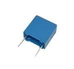
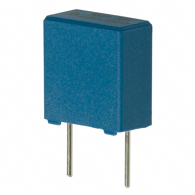
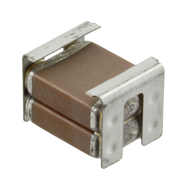
| 描述 | CAP FILM 0.022UF 400VDC RADIAL |
| ESR(等效串联电阻) | - |
| 产品分类 | |
| 品牌 | EPCOS Inc |
| 数据手册 | |
| 产品图片 |
|
| 产品型号 | B32620A4223K189 |
| PCN设计/规格 | |
| rohs | 无铅 / 符合限制有害物质指令(RoHS)规范要求 |
| 产品系列 | B32620 |
| 产品目录绘图 |
|
| 介电材料 | 聚丙烯(PP), 金属化 |
| 其它名称 | 495-4988-2 |
| 包装 | 带卷 (TR) |
| 大小/尺寸 | 0.394" 长 x 0.197" 宽(10.00mm x 5.00mm) |
| 安装类型 | 通孔 |
| 容差 | ±10% |
| 封装/外壳 | 径向 |
| 工作温度 | -55°C ~ 105°C |
| 应用 | 高脉冲,DV/DT |
| 引线间距 | 0.295"(7.50mm) |
| 标准包装 | 1,400 |
| 特性 | - |
| 电容 | 0.022µF |
| 端接 | PC 引脚 |
| 额定电压-AC | 200V |
| 额定电压-DC | 400V |
| 高度-安装(最大值) | 0.413"(10.50mm) |


PDF Datasheet 数据手册内容提取
Film Capacitors Metallized Polypropylene Film Capacitors (MKP) Series/Type: B32620, B32621 Date: June 2018 ©EPCOSAG2018.Reproduction,publicationanddisseminationofthispublication,enclosuresheretoandthe informationcontainedthereinwithoutEPCOS'priorexpressconsentisprohibited. EPCOSAGisaTDKGroupCompany.
Metallized polypropylene film capacitors (MKP) B32620, B32621 High pulse (stacked) Typical applications Dimensional drawing Compact fluorescent lamps (CFL) SMPS Climatic Max. operating temperature: 105 °C Climatic category (IEC 60068-1:2013): 55/100/56 Construction Dielectric: polypropylene (PP) Stacked-film technology Plastic case (UL 94 V-0) Dimensions in mm Epoxy resin sealing Lead spacing Lead diameter Type Features ±0.4 d ±0.05 Very high pulse strength 1 7.5 0.5 B32620 Very good self-healing properties 10.0 0.61) B32621 Smallest possible dimensions High contact reliability 1) 0.5mmforcapacitorwidthw=4mm RoHS-compatible Terminals Parallel wire leads, lead-free tinned Special lead lengths available on request Marking Manufacturer's logo, rated capacitance (coded), cap. tolerance (code letter), rated voltage, date of manufacture (coded), for lead spacing 7.5 mm: style (MKP), for lead spacing 10 mm: lot number, series number (621) Delivery mode Bulk (untaped) Taped (Ammo pack or reel) For notes on taping, refer to chapter "Taping and packing“. PleasereadCautionsandwarningsand Page2of30 Importantnotesattheendofthisdocument.
B32620, B32621 High pulse (stacked) Overview of available types Lead spacing 7.5 mm 10.0 mm Type B32620 B32621 Page 4 6 V (V DC) 160 250 400 630 1000 1000 160 250 400 630 1000 R V (V AC) 90 140 200 400 500 600 90 140 200 400 500 RMS C (nF) R 1.0 1.5 2.2 3.3 4.7 6.8 10 15 22 33 47 68 100 150 220 PleasereadCautionsandwarningsand Page3of30 Importantnotesattheendofthisdocument.
B32620 High pulse (stacked) Ordering codes and packing units (lead spacing 7.5 mm) V V C Max. dimensions Ordering code Ammo Reel Untaped R RMS R f ≤1 kHz w × h × l (composition see pack V DC V AC nF mm below) pcs./MOQ pcs./MOQ pcs./MOQ 160 90 33 4.0 × 8.5 × 10.0 B32620A5333+*** 8000 7200 6000 47 4.0 × 8.5 × 10.0 B32620A5473+*** 8000 7200 6000 68 5.0 × 10.5 × 10.0 B32620A5683+*** 6400 5600 4000 100 5.0 × 10.5 × 10.0 B32620A5104+*** 6400 5600 4000 150 6.0 × 12.0 × 10.3 B32620A5154+*** 5200 4400 3000 250 140 22 4.0 × 8.5 × 10.0 B32620A3223+*** 8000 7200 6000 33 4.0 × 8.5 × 10.0 B32620A3333+*** 8000 7200 6000 47 5.0 × 10.5 × 10.0 B32620A3473+*** 6400 5600 4000 68 5.0 × 10.5 × 10.0 B32620A3683+*** 6400 5600 4000 100 6.0 × 12.0 × 10.3 B32620A3104+*** 5200 4400 3000 400 200 6.8 4.0 × 8.5 × 10.0 B32620A4682+*** 8000 7200 6000 10 4.0 × 8.5 × 10.0 B32620A4103+*** 8000 7200 6000 15 5.0 × 10.5 × 10.0 B32620A4153+*** 6400 5600 4000 22 5.0 × 10.5 × 10.0 B32620A4223+*** 6400 5600 4000 33 6.0 × 12.0 × 10.3 B32620A4333+*** 5200 4400 3000 630 400 1.5 4.0 × 8.5 × 10.0 B32620A6152+*** 8000 7200 6000 2.2 4.0 × 8.5 × 10.0 B32620A6222+*** 8000 7200 6000 3.3 4.0 × 8.5 × 10.0 B32620A6332+*** 8000 7200 6000 4.7 4.0 × 8.5 × 10.0 B32620A6472+*** 8000 7200 6000 6.8 5.0 × 10.5 × 10.0 B32620A6682+*** 6400 5600 4000 10 5.0 × 10.5 × 10.0 B32620A6103+*** 6400 5600 4000 15 6.0 × 12.0 × 10.3 B32620A6153+*** 5200 4400 3000 MOQ = Minimum Order Quantity, consisting of 4 packing units. Further E series and intermediate capacitance values on request. Compositionoforderingcode += Capacitancetolerancecode: ***= Packagingcode: K= ±10% 289= Straightterminals,Ammopack J= ±5% 189= Straightterminals,Reel 000= Straightterminals,Untaped(standardlead length6(cid:4)1mm) PleasereadCautionsandwarningsand Page4of30 Importantnotesattheendofthisdocument.
B32620 High pulse (stacked) Ordering codes and packing units (lead spacing 7.5 mm) V V C Max. dimensions Ordering code Ammo Reel Untaped R RMS R f ≤1 kHz w × h × l (composition see pack V DC V AC nF mm below) pcs./MOQ pcs./MOQ pcs./MOQ 1000 500 1.5 4.0 × 8.5 × 10.0 B32620A0152+*** 8000 7200 6000 2.2 4.0 × 8.5 × 10.0 B32620A0222+*** 8000 7200 6000 3.3 5.0 × 10.5 × 10.0 B32620A0332+*** 6400 5600 4000 4.7 5.0 × 10.5 × 10.0 B32620A0472+*** 6400 5600 4000 6.8 6.0 × 12.0 × 10.3 B32620A0682+*** 5200 4400 3000 1000 600 1.0 5.0 × 10.5 × 10.0 B32620J0102+*** 6400 5600 4000 1.5 5.0 × 10.5 × 10.0 B32620J0152+*** 6400 5600 4000 2.2 5.0 × 10.5 × 10.0 B32620J0222+*** 6400 5600 4000 3.3 5.0 × 10.5 × 10.0 B32620J0332+*** 6400 5600 4000 4.7 6.0 × 12.0 × 10.3 B32620J0472+*** 5200 4400 3000 MOQ = Minimum Order Quantity, consisting of 4 packing units. Further E series and intermediate capacitance values on request. Compositionoforderingcode += Capacitancetolerancecode: ***= Packagingcode: K= ±10% 289= Straightterminals,Ammopack J= ±5% 189= Straightterminals,Reel 000= Straightterminals,Untaped(standardlead length6(cid:4)1mm) PleasereadCautionsandwarningsand Page5of30 Importantnotesattheendofthisdocument.
B32621 High pulse (stacked) Ordering codes and packing units (lead spacing 10 mm) V V C Max. dimensions Ordering code Ammo Reel Untaped R RMS R f ≤1 kHz w × h × l (composition see pack V DC V AC nF mm below) pcs./MOQ pcs./MOQ pcs./MOQ 160 90 47 4.0 × 7.0 × 13.0 B32621A5473+*** 4000 6800 4000 68 4.0 × 9.0 × 13.0 B32621A5683+*** 4000 6800 4000 100 5.0 × 11.0 × 13.0 B32621A5104+*** 3320 5200 4000 150 5.0 × 11.0 × 13.0 B32621A5154+*** 3320 5200 4000 220 6.0 × 12.0 × 13.0 B32621A5224+*** 2720 4400 4000 250 140 2.2 4.0 × 7.0 × 13.0 B32621A3222+*** 4000 6800 4000 3.3 4.0 × 9.0 × 13.0 B32621A3332+*** 4000 6800 4000 4.7 4.0 × 9.0 × 13.0 B32621A3472+*** 4000 6800 4000 6.8 4.0 × 9.0 × 13.0 B32621A3682+*** 4000 6800 4000 10 4.0 × 9.0 × 13.0 B32621A3103+*** 4000 6800 4000 15 4.0 × 9.0 × 13.0 B32621A3153+*** 4000 6800 4000 22 4.0 × 9.0 × 13.0 B32621A3223+*** 4000 6800 4000 33 4.0 × 9.0 × 13.0 B32621A3333+*** 4000 6800 4000 47 4.0 × 9.0 × 13.0 B32621A3473+*** 4000 6800 4000 68 5.0 × 11.0 × 13.0 B32621A3683+*** 3320 5200 4000 100 6.0 × 12.0 × 13.0 B32621A3104+*** 2720 4400 4000 400 200 10 4.0 × 9.0 × 13.0 B32621A4103+*** 4000 6800 4000 15 4.0 × 9.0 × 13.0 B32621A4153+*** 4000 6800 4000 22 5.0 × 11.0 × 13.0 B32621A4223+*** 3320 5200 4000 33 5.0 × 11.0 × 13.0 B32621A4333+*** 3320 5200 4000 47 6.0 × 12.0 × 13.0 B32621A4473+*** 2720 4400 4000 MOQ = Minimum Order Quantity, consisting of 4 packing units. Intermediate capacitances values on request. Compositionoforderingcode += Capacitancetolerancecode: ***= Packagingcode: K= ±10% 289= Straightterminals,Ammopack J= ±5% 189= Straightterminals,Reel 000= Straightterminals,Untaped(standardlead length6(cid:4)1mm) PleasereadCautionsandwarningsand Page6of30 Importantnotesattheendofthisdocument.
B32621 High pulse (stacked) Ordering codes and packing units (lead spacing 10 mm) V V C Max. dimensions Ordering code Ammo Reel Untaped R RMS R f ≤1 kHz w × h × l (composition see pack V DC V AC nF mm below) pcs./MOQ pcs./MOQ pcs./MOQ 630 400 2.2 4.0 × 7.0 × 13.0 B32621A6222+*** 4000 6800 4000 3.3 4.0 × 9.0 × 13.0 B32621A6332+*** 4000 6800 4000 4.7 4.0 × 9.0 × 13.0 B32621A6472+*** 4000 6800 4000 6.8 4.0 × 9.0 × 13.0 B32621A6682+*** 4000 6800 4000 10 4.0 × 9.0 × 13.0 B32621A6103+*** 4000 6800 4000 15 5.0 × 11.0 × 13.0 B32621A6153+*** 3320 5200 4000 22 6.0 × 12.0 × 13.0 B32621A6223+*** 2720 4400 4000 33 6.0 × 12.0 × 13.0 B32621A6333+*** 2720 4400 4000 1000 500 2.2 4.0 × 7.0 × 13.0 B32621A0222+*** 4000 6800 4000 3.3 4.0 × 9.0 × 13.0 B32621A0332+*** 4000 6800 4000 4.7 4.0 × 9.0 × 13.0 B32621A0472+*** 4000 6800 4000 6.8 5.0 × 11.0 × 13.0 B32621A0682+*** 3320 5200 4000 10 6.0 × 12.0 × 13.0 B32621A0103+*** 2720 4400 4000 MOQ = Minimum Order Quantity, consisting of 4 packing units. Intermediate capacitances values on request. Compositionoforderingcode += Capacitancetolerancecode: ***= Packagingcode: K= ±10% 289= Straightterminals,Ammopack J= ±5% 189= Straightterminals,Reel 000= Straightterminals,Untaped(standardlead length6(cid:4)1mm) PleasereadCautionsandwarningsand Page7of30 Importantnotesattheendofthisdocument.
B32620, B32621 High pulse (stacked) Technical data Operating temperature range Max. operating temperature T +105 °C op,max Upper category temperature T +100 °C max Lower category temperature Tmin (cid:4)55 °C Rated temperature T +85 °C R Dissipation factor tan δ (in 10-3) at C ≤ 0.1 μF 0.1 μF < C ≤ 0.22 μF R R at 20 °C (upper limit values) 1 kHz (cid:4) 1.0 10 kHz (cid:4) 1.5 100 kHz 4.0 (cid:4) Insulation resistance R at 100 GΩ ins 20 °C, rel. humidity ≤ 65% (minimum as-delivered values) DC test voltage 1.6 (cid:5) VR, 2 s Category voltage V T (°C) DC voltage derating AC voltage derating C op (continuous operation with T ≤ 85 V = V V =V op C R C,RMS RMS VDC or VAC at f ≤ 1 kHz) 85<Top ≤100 VC = VR(cid:5)(165 - Top)/80 VC,RMS=VRMS(cid:5)(165-Top)/80 Operating voltage V for short T (°C) DC voltage (max. hrs.) AC voltage (max. hrs.) op op operating periods Top ≤ 85 Vop = 1.25(cid:5)VC(2000 h) Vop = 1.0(cid:5)VC,RMS(2000 h) (VDCor VAC at f ≤ 1 kHz) 85<Top≤100 Vop = 1.25(cid:5)VC(1000 h) Vop = 1.0(cid:5)VC,RMS(1000 h) Damp heat test 56 days/40 °C/93% relative humidity Limit values after damp heat Capacitance change (cid:6)ΔC/C(cid:6) ≤ 3% test Dissipation factor change Δ tan δ ≤ 0.5 (cid:5) 10-3 (at 1 kHz) ≤ 1.0 (cid:5) 10-3 (at 10 kHz) Insulation resistance R ≥ 50% of minimum ins as-delivered values Reliability: Failure rate λ 1 fit (≤ 1 (cid:5) 10-9/h) at 0.5 (cid:5) VR, 40 °C Service life tSL 200 000 h at 1.0 (cid:5) VR, 85 °C For conversion to other operating conditions and temperatures, refer to chapter "Quality, 2 Reliability". Failure criteria: Total failure Short circuit or open circuit Failure due to variation Capacitance change (cid:6)ΔC/C(cid:6) > ±10% of parameters Dissipation factor tan δ > 4 (cid:5) upper limit value Insulation resistance R < 1500 MΩ ins PleasereadCautionsandwarningsand Page8of30 Importantnotesattheendofthisdocument.
B32620, B32621 High pulse (stacked) Pulse handling capability "dV/dt" represents the maximum permissible voltage change per unit of time for non-sinusoidal voltages, expressed in V/μs. "k " represents the maximum permissible pulse characteristic of the waveform applied to the 0 capacitor, expressed in V2/μs. Note: The values of dV/dt and k provided below must not be exceeded in order to avoid damaging the 0 capacitor. dV/dt values Lead spacing 7.5 mm 10 mm V V R RMS V DC V AC dV/dt in V/μs 160 90 750 600 250 140 1 200 900 400 200 1 500 1 050 630 400 2 700 1 800 1 000 500 3 200 2 400 1 000 600 4 000 (cid:4) k values 0 Lead spacing 7.5 mm 10 mm V V R RMS V DC V AC k in V2/μs 0 160 90 240 000 190 000 250 140 600 000 450 000 400 200 1 200 000 840 000 630 400 3 400 000 2 250 000 1 000 500 6 400 000 4 800 000 1 000 600 8 000 000 (cid:4) PleasereadCautionsandwarningsand Page9of30 Importantnotesattheendofthisdocument.
B32620, B32621 High pulse (stacked) Impedance Z versus frequency f (typical values) PleasereadCautionsandwarningsand Page10of30 Importantnotesattheendofthisdocument.
B32620 High pulse (stacked) Permissible AC voltage V versus frequency f (for sinusoidal waveforms, T ≤90 °C) RMS A For T >90 °C, please refer to "General technical information", section 3.2.3. A Lead spacing 7.5 mm 160 V DC/90 V AC 250 V DC/140 V AC 400 V DC/200 V AC 630 V DC/400 V AC PleasereadCautionsandwarningsand Page11of30 Importantnotesattheendofthisdocument.
B32620 High pulse (stacked) Permissible AC voltage V versus frequency f (for sinusoidal waveforms, T ≤90 °C) RMS A For T >90 °C, please refer to "General technical information", section 3.2.3. A Lead spacing 7.5 mm 1000 V DC/500 V AC 1000 V DC/600 V AC PleasereadCautionsandwarningsand Page12of30 Importantnotesattheendofthisdocument.
B32621 High pulse (stacked) Permissible AC voltage V versus frequency f (for sinusoidal waveforms, T ≤90 °C) RMS A For T >90 °C, please refer to "General technical information", section 3.2.3. A Lead spacing 10 mm 160 V DC/90 V AC 250 V DC/140 V AC 400 V DC/200 V AC 630 V DC/400 V AC PleasereadCautionsandwarningsand Page13of30 Importantnotesattheendofthisdocument.
B32621 High pulse (stacked) Permissible AC voltage V versus frequency f (for sinusoidal waveforms, T ≤90 °C) RMS A For T >90 °C, please refer to "General technical information", section 3.2.3. A Lead spacing 10 mm 1000 V DC/500 V AC PleasereadCautionsandwarningsand Page14of30 Importantnotesattheendofthisdocument.
B32620, B32621 High pulse (stacked) Sinus-wave application, lighting Permissible voltage and current / waveform PleasereadCautionsandwarningsand Page15of30 Importantnotesattheendofthisdocument.
B32620 High pulse (stacked) Sinus-wave application, lighting Permissible current I versus rated capacitance C pp R Lead spacing 7.5 mm 160 V DC/90 V AC 250 V DC/140 V AC 400 V DC/200 V AC 630 V DC/400 V AC PleasereadCautionsandwarningsand Page16of30 Importantnotesattheendofthisdocument.
B32620 High pulse (stacked) Sinus-wave application, lighting Permissible current I versus rated capacitance C pp R Lead spacing 7.5 mm 1000 V DC/500 V AC 1000 V DC/600 V AC PleasereadCautionsandwarningsand Page17of30 Importantnotesattheendofthisdocument.
B32621 High pulse (stacked) Sinus-wave application, lighting Permissible current I versus rated capacitance C pp R Lead spacing 10 mm 160 V DC/90 V AC 250 V DC/140 V AC 400 V DC/200 V AC 630 V DC/400 V AC PleasereadCautionsandwarningsand Page18of30 Importantnotesattheendofthisdocument.
B32621 High pulse (stacked) Sinus-wave application, lighting Permissible current I versus rated capacitance C pp R Lead spacing 10 mm 1000 V DC/500 V AC PleasereadCautionsandwarningsand Page19of30 Importantnotesattheendofthisdocument.
B32620, B32621 High pulse (stacked) Mounting guidelines 1 Soldering 1.1 Solderability of leads The solderability of terminal leads is tested to IEC 60068-2-20:2008, test Ta, method 1. Before a solderability test is carried out, terminals are subjected to accelerated ageing (to IEC 60068-2-2:2007, test Ba: 4 h exposure to dry heat at 155 °C). Since the ageing temperature is far higher than the upper category temperature of the capacitors, the terminal wires should be cut off from the capacitor before the ageing procedure to prevent the solderability being impaired by the products of any capacitor decomposition that might occur. Solder bath temperature 235 ±5 °C Soldering time 2.0 ±0.5 s Immersion depth 2.0 +0/(cid:4)0.5 mm from capacitor body or seating plane Evaluation criteria: Wetting of wire surface by new solder ≥90%, Visual inspection free-flowing solder 1.2 Resistance to soldering heat Resistance to soldering heat is tested to IEC 60068-2-20:2008, test Tb, method 1. Conditions: Series Solder bath temperature Soldering time MKT boxed (except 2.5 × 6.5 × 7.2 mm) 260 ±5 °C 10 ±1 s coated uncoated (lead spacing >10 mm) MFP MKP (lead spacing >7.5 mm) MKT boxed (case 2.5 × 6.5 × 7.2 mm) 5 ±1 s MKP (lead spacing ≤7.5 mm) <4 s MKT uncoated (lead spacing ≤10 mm) recommended soldering insulated (B32559) profile for MKT uncoated (lead spacing ≤ 10 mm) and insulated (B32559) PleasereadCautionsandwarningsand Page20of30 Importantnotesattheendofthisdocument.
B32620, B32621 High pulse (stacked) Immersion depth 2.0 +0/(cid:4)0.5 mm from capacitor body or seating plane Shield Heat-absorbing board, (1.5 ±0.5) mm thick, between capacitor body and liquid solder Evaluation criteria: Visual inspection No visible damage 2% for MKT/MKP/MFP ΔC/C 0 5% for EMI suppression capacitors tan δ As specified in sectional specification 1.3 General notes on soldering Permissible heat exposure loads on film capacitors are primarily characterized by the upper cate- gory temperature T . Long exposure to temperatures above this type-related temperature limit max can lead to changes in the plastic dielectric and thus change irreversibly a capacitor's electrical characteristics. For short exposures (as in practical soldering processes) the heat load (and thus the possible effects on a capacitor) will also depend on other factors like: Pre-heating temperature and time Forced cooling immediately after soldering Terminal characteristics: diameter, length, thermal resistance, special configurations (e.g. crimping) Height of capacitor above solder bath Shadowing by neighboring components Additional heating due to heat dissipation by neighboring components Use of solder-resist coatings PleasereadCautionsandwarningsand Page21of30 Importantnotesattheendofthisdocument.
B32620, B32621 High pulse (stacked) The overheating associated with some of these factors can usually be reduced by suitable coun- termeasures. For example, if a pre-heating step cannot be avoided, an additional or reinforced cooling process may possibly have to be included. EPCOS recommendations As a reference, the recommended wave soldering profile for our film capacitors is as follows: PleasereadCautionsandwarningsand Page22of30 Importantnotesattheendofthisdocument.
B32620, B32621 High pulse (stacked) Body temperature should follow the description below: MKP capacitor During pre-heating: T ≤110 °C p During soldering: T ≤120 °C, t ≤45 s s s MKT capacitor During pre-heating: T ≤125 °C p During soldering: T ≤160 °C, t ≤45 s s s When SMD components are used together with leaded ones, the film capacitors should not pass into the SMD adhesive curing oven. The leaded components should be assembled after the SMD curing step. Leaded film capacitors are not suitable for reflow soldering. In order to ensure proper conditions for manual or selective soldering, the body temperature of the capacitor (T ) must be ≤120 °C. s One recommended condition for manual soldering is that the tip of the soldering iron should be <360 °C and the soldering contact time should be no longer than 3 seconds. For uncoated MKT capacitors with lead spacings ≤10 mm (B32560/B32561) the following mea- sures are recommended: pre-heating to not more than 110 °C in the preheater phase rapid cooling after soldering Please refer to EPCOS Film Capacitor Data Book in case more details are needed. PleasereadCautionsandwarningsand Page23of30 Importantnotesattheendofthisdocument.
B32620, B32621 High pulse (stacked) Cautions and warnings Do not exceed the upper category temperature (UCT). Do not apply any mechanical stress to the capacitor terminals. Avoid any compressive, tensile or flexural stress. Do not move the capacitor after it has been soldered to the PC board. Do not pick up the PC board by the soldered capacitor. Do not place the capacitor on a PC board whose PTH hole spacing differs from the specified lead spacing. Do not exceed the specified time or temperature limits during soldering. Avoid external energy inputs, such as fire or electricity. Avoid overload of the capacitors. Consult us if application is with severe temperature and humidity condition. There are no serviceable or repairable parts inside the capacitor. Opening the capacitor or any attempts to open or repair the capacitor will void the warranty and liability of EPCOS. Please note that the standards referred to in this publication may have been revised in the meantime. The table below summarizes the safety instructions that must always be observed. A detailed de- scription can be found in the relevant sections of the chapters "General technical information" and "Mounting guidelines". Topic Safety information Reference chapter "General technical information" Storage Make sure that capacitors are stored within the specified 4.5 conditions range of time, temperature and humidity conditions. "Storage conditions" Flammability Avoid external energy, such as fire or electricity (passive 5.3 flammability), avoid overload of the capacitors (active "Flammability" flammability) and consider the flammability of materials. Resistance to Do not exceed the tested ability to withstand vibration. 5.2 vibration The capacitors are tested to IEC 60068-2-6:2007. "Resistance to EPCOS offers film capacitors specially designed for vibration" operation under more severe vibration regimes such as those found in automotive applications. Consult our catalog "Film Capacitors for Automotive Electronics". Topic Safety information Reference chapter "Mounting guidelines" Soldering Do not exceed the specified time or temperature limits 1 "Soldering" during soldering. Cleaning Use only suitable solvents for cleaning capacitors. 2 "Cleaning" PleasereadCautionsandwarningsand Page24of30 Importantnotesattheendofthisdocument.
B32620, B32621 High pulse (stacked) Topic Safety information Reference chapter "Mounting guidelines" Embedding of When embedding finished circuit assemblies in plastic 3 "Embedding of capacitors in resins, chemical and thermal influences must be taken capacitors in finished finished into account. assemblies" assemblies Caution: Consult us first, if you also wish to embed other uncoated component types! Display of ordering codes for EPCOS products The ordering code for one and the same product can be represented differently in data sheets, data books, other publications and the website of EPCOS, or in order-related documents such as shipping notes, order confirmations and product labels. The varying representations of the or- dering codes are due to different processes employed and do not affect the specifications of the respective products. Detailed information can be found on the Internet under www.epcos.com/orderingcodes. PleasereadCautionsandwarningsand Page25of30 Importantnotesattheendofthisdocument.
B32620, B32621 High pulse (stacked) Symbols and terms Symbol English German α Heat transfer coefficient Wärmeübergangszahl α Temperature coefficient of capacitance Temperaturkoeffizient der Kapazität C A Capacitor surface area Kondensatoroberfläche β Humidity coefficient of capacitance Feuchtekoeffizient der Kapazität C C Capacitance Kapazität C Rated capacitance Nennkapazität R ΔC Absolute capacitance change Absolute Kapazitätsänderung ΔC/C Relative capacitance change (relative Relative Kapazitätsänderung (relative deviation of actual value) Abweichung vom Ist-Wert) ΔC/C Capacitance tolerance (relative deviation Kapazitätstoleranz (relative Abweichung R from rated capacitance) vom Nennwert) dt Time differential Differentielle Zeit Δt Time interval Zeitintervall ΔT Absolute temperature change Absolute Temperaturänderung (self-heating) (Selbsterwärmung) Δtan δ Absolute change of dissipation factor Absolute Änderung des Verlustfaktors ΔV Absolute voltage change Absolute Spannungsänderung dV/dt Time differential of voltage function (rate Differentielle Spannungsänderung of voltage rise) (Spannungsflankensteilheit) ΔV/Δt Voltage change per time interval Spannungsänderung pro Zeitintervall E Activation energy for diffusion Aktivierungsenergie zur Diffusion ESL Self-inductance Eigeninduktivität ESR Equivalent series resistance Ersatz-Serienwiderstand f Frequency Frequenz f Frequency limit for reducing permissible Grenzfrequenz für thermisch bedingte 1 AC voltage due to thermal limits Reduzierung der zulässigen Wechselspannung f Frequency limit for reducing permissible Grenzfrequenz für strombedingte 2 AC voltage due to current limit Reduzierung der zulässigen Wechselspannung f Resonant frequency Resonanzfrequenz r F Thermal acceleration factor for diffusion Therm. Beschleunigungsfaktor zur D Diffusion F Derating factor Deratingfaktor T i Current (peak) Stromspitze I Category current (max. continuous Kategoriestrom (max. Dauerstrom) C current) PleasereadCautionsandwarningsand Page26of30 Importantnotesattheendofthisdocument.
B32620, B32621 High pulse (stacked) Symbol English German I (Sinusoidal) alternating current, (Sinusförmiger) Wechselstrom RMS root-mean-square value i Capacitance drift Inkonstanz der Kapazität z k Pulse characteristic Impulskennwert 0 L Series inductance Serieninduktivität S λ Failure rate Ausfallrate λ Constant failure rate during useful Konstante Ausfallrate in der 0 service life Nutzungsphase λ Failure rate, determined by tests Experimentell ermittelte Ausfallrate test P Dissipated power Abgegebene Verlustleistung diss P Generated power Erzeugte Verlustleistung gen Q Heat energy Wärmeenergie ρ Density of water vapor in air Dichte von Wasserdampf in Luft R Universal molar constant for gases Allg. Molarkonstante für Gas R Ohmic resistance of discharge circuit Ohmscher Widerstand des Entladekreises R Internal resistance Innenwiderstand i R Insulation resistance Isolationswiderstand ins R Parallel resistance Parallelwiderstand P R Series resistance Serienwiderstand S S severity (humidity test) Schärfegrad (Feuchtetest) t Time Zeit T Temperature Temperatur τ Time constant Zeitkonstante tan δ Dissipation factor Verlustfaktor tan δ Dielectric component of dissipation Dielektrischer Anteil des Verlustfaktors D factor tan δ Parallel component of dissipation factor Parallelanteil des Verlfustfaktors P tan δ Series component of dissipation factor Serienanteil des Verlustfaktors S T Temperature of the air surrounding the Temperatur der Luft, die das Bauteil A component umgibt T Upper category temperature Obere Kategorietemperatur max T Lower category temperature Untere Kategorietemperatur min t Operating life at operating temperature Betriebszeit bei Betriebstemperatur und OL and voltage -spannung T Operating temperature, T + ΔT Beriebstemperatur, T + ΔT op A A T Rated temperature Nenntemperatur R T Reference temperature Referenztemperatur ref t Reference service life Referenz-Lebensdauer SL PleasereadCautionsandwarningsand Page27of30 Importantnotesattheendofthisdocument.
B32620, B32621 High pulse (stacked) Symbol English German V AC voltage Wechselspannung AC V Category voltage Kategoriespannung C V Category AC voltage (Sinusförmige) C,RMS Kategorie-Wechselspannung V Corona-discharge onset voltage Teilentlade-Einsatzspannung CD V Charging voltage Ladespannung ch V DC voltage Gleichspannung DC V Fly-back capacitor voltage Spannung (Flyback) FB V Input voltage Eingangsspannung i V Output voltage Ausgangssspannung o V Operating voltage Betriebsspannung op V Peak pulse voltage Impuls-Spitzenspannung p V Peak-to-peak voltage Impedance Spannungshub pp V Rated voltage Nennspannung R Amplitude of rated AC voltage Amplitude der Nenn-Wechselspannung R V (Sinusoidal) alternating voltage, (Sinusförmige) Wechselspannung RMS root-mean-square value V S-correction voltage Spannung bei Anwendung "S-correction" SC V Snubber capacitor voltage Spannung bei Anwendung sn "Beschaltung" Z Impedance Scheinwiderstand Lead spacing Rastermaß PleasereadCautionsandwarningsand Page28of30 Importantnotesattheendofthisdocument.
Important notes The following applies to all products named in this publication: 1. Some parts of this publication contain statements about the suitability of our products for certain areas of application. These statements are based on our knowledge of typical re- quirements that are often placed on our products in the areas of application concerned. We nevertheless expressly point out that such statements cannot be regarded as binding statements about the suitability of our products for a particular customer application. As a rule, EPCOS is either unfamiliar with individual customer applications or less familiar with them than the customers themselves. For these reasons, it is always ultimately incum- bent on the customer to check and decide whether an EPCOS product with the properties de- scribed in the product specification is suitable for use in a particular customer application. 2. We also point out that in individual cases, a malfunction of electronic components or failure before the end of their usual service life cannot be completely ruled out in the current state of the art, even if they are operated as specified. In customer applications requiring a very high level of operational safety and especially in customer applications in which the malfunction or failure of an electronic component could endanger human life or health (e.g. in accident prevention or lifesaving systems), it must therefore be ensured by means of suitable design of the customer application or other action taken by the customer (e.g. installation of protective circuitry or redundancy) that no injury or damage is sustained by third parties in the event of malfunction or failure of an electronic component. 3. The warnings, cautions and product-specific notes must be observed. 4. In order to satisfy certain technical requirements, some of the products described in this publication may contain substances subject to restrictions in certain jurisdictions (e.g. because they are classed as hazardous). Useful information on this will be found in our Ma- terial Data Sheets on the Internet (www.epcos.com/material). Should you have any more de- tailed questions, please contact our sales offices. 5. We constantly strive to improve our products. Consequently, the products described in this publication may change from time to time. The same is true of the corresponding product specifications. Please check therefore to what extent product descriptions and specifications contained in this publication are still applicable before or when you place an order. We also reserve the right to discontinue production and delivery of products. Consequently, we cannot guarantee that all products named in this publication will always be available. The aforementioned does not apply in the case of individual agreements deviating from the fore- going for customer-specific products. 6. Unless otherwise agreed in individual contracts, all orders are subject to the current ver- sion of the "General Terms of Delivery for Products and Services in the Electrical In- dustry" published by the German Electrical and Electronics Industry Association (ZVEI). Page29of30
Important notes 7. Our manufacturing sites serving the automotive business apply the IATF 16949 standard. The IATF certifications confirm our compliance with requirements regarding the quality management system in the automotive industry. Referring to customer requirements and customer specific requirements (“CSR”) TDK always has and will continue to have the policy of respecting individual agreements. Even if IATF 16949 may appear to support the acceptance of unilateral requirements, we hereby like to emphasize that only requirements mutually agreed upon can and will be implemented in our Quality Management System. For clarification purposes we like to point out that obligations from IATF 16949 shall only become legally binding if individually agreed upon. 8. The trade names EPCOS, CeraCharge, CeraDiode, CeraLink, CeraPad, CeraPlas, CSMP, CTVS, DeltaCap, DigiSiMic, ExoCore, FilterCap, FormFit, LeaXield, MiniBlue, MiniCell, MKD, MKK, MotorCap, PCC, PhaseCap, PhaseCube, PhaseMod, PhiCap, PowerHap, PQSine, PQvar, SIFERRIT, SIFI, SIKOREL, SilverCap, SIMDAD, SiMic, SIMID, SineFormer, SIOV, ThermoFuse, WindCap are trademarks registered or pending in Europe and in other coun- tries. Further information will be found on the Internet at www.epcos.com/trademarks. Release 2018-06 Page30of30
Mouser Electronics Authorized Distributor Click to View Pricing, Inventory, Delivery & Lifecycle Information: E PCOS / TDK: B32621A3473K289 B32621A3683K289 B32621A6332K289 B32621A6682K289 B32621A6333K289 B32620A5333J289 B32620A5104J289 B32620A5154J289 B32620A4333J289 B32620A6152J289 B32620A272K289 B32620A3123J B32620A3513J189 B32620A3823J289 B32620A4123J289 B32620A4183J289 B32620A4273J289 B32620A4392J289 B32620A4393J289 B32620A4562J289 B32620A4622J B32620A4682K B32620A472K189 B32620A562J189 B32620A6122K B32620A6182J289 B32620A6272J B32620A6272J289 B32620A6392J289 B32620A6471K289 B32620A6562J289 B32620J272J189 B32620J392J289 B32620J821J B32621A3103K B32621A3333K B32621A392K B32621A392K289 B32621A4273J B32621A4273J289 B32621A5154K B32621A5683K B32621A5823J289 B32621A6183J189 B32621A6183K289 B32621A6203J289 B32621A6203K289 B32621A6273J B32621A6273K B32621A822K289 B32620A6123J289 B32620A152J B32620A152J289 B32620A152K B32620A222J B32620A222K B32620A222K189 B32620A222K289 B32620A302J B32620A3104J B32620A3104J289 B32620A3104K B32620A3104K189 B32620A3104K289 B32620A3223J B32620A332J B32620A332J189 B32620A332J289 B32620A332K289 B32620A3333J189 B32620A3333K B32620A3333K189 B32620A3333K289 B32620A3473J B32620A3473J189 B32620A3473J289 B32620A3473K B32620A3473K189 B32620A3683J B32620A3683J289 B32620A3683K B32620A3683K289 B32620A4103J B32620A4103J289 B32620A4103K B32620A4103K289 B32620A4123K289 B32620A4153J B32620A4153J289 B32620A4153K B32620A4153K189 B32620A4223J B32620A4223J289 B32620A4223K B32620A4223K189 B32620A4332J289 B32620A4333J B32620A4333K B32620A4333K289 B32620A4472J289