ICGOO在线商城 > 集成电路(IC) > 接口 - 传感器,电容式触摸 > AT42QT1010-TSHR
/AT42QT1010-TSHR.jpg)
 Datasheet下载
- 型号: AT42QT1010-TSHR
- 制造商: Atmel
- 库位|库存: xxxx|xxxx
- 要求:
| 数量阶梯 | 香港交货 | 国内含税 |
| +xxxx | $xxxx | ¥xxxx |
查看当月历史价格
查看今年历史价格
AT42QT1010-TSHR产品简介:
ICGOO电子元器件商城为您提供AT42QT1010-TSHR由Atmel设计生产,在icgoo商城现货销售,并且可以通过原厂、代理商等渠道进行代购。 AT42QT1010-TSHR价格参考。AtmelAT42QT1010-TSHR封装/规格:接口 - 传感器,电容式触摸, Capacitive Touch Buttons SOT-23-6。您可以下载AT42QT1010-TSHR参考资料、Datasheet数据手册功能说明书,资料中有AT42QT1010-TSHR 详细功能的应用电路图电压和使用方法及教程。
Microchip Technology的AT42QT1010-TSHR是一款电容式触摸传感器接口芯片,主要用于实现单通道电容式触摸感应功能。它广泛应用于各种消费电子、家电、工业控制和汽车电子等领域,特别是在需要简单触摸控制的场景中。

 应用场景:

1. 家用电器:
   - 该芯片常用于洗衣机、冰箱、微波炉等家电产品的控制面板上,替代传统的机械按钮。用户可以通过轻触面板来选择不同的功能或调整设置,提升操作的便捷性和美观度。
   - 在空调遥控器或壁挂式控制器中,AT42QT1010-TSHR可以提供简洁的触摸按键设计,增强用户体验。

2. 消费电子产品:
   - 在便携式音乐播放器、智能音箱、耳机充电盒等设备中,该芯片可以用于实现触摸控制功能,如播放/暂停、音量调节等。
   - 它还可以用于智能家居设备,如智能灯控开关、门锁等,通过触摸感应实现无接触操作,提升设备的智能化水平。

3. 工业控制与自动化:
   - 在工业设备的操作面板上,AT42QT1010-TSHR可以用于实现触摸式按钮,帮助操作人员更方便地进行设备控制和参数设置。
   - 它也可以集成到人机界面(HMI)系统中,提供更加直观的操作方式,减少误操作的可能性。

4. 汽车电子:
   - 在汽车内部,该芯片可以用于中控台、车窗控制、后视镜调节等位置,提供触摸感应功能,提升驾驶体验和安全性。
   - 它还可以用于车内照明系统的触摸控制,使用户能够通过轻触面板来开关灯光或调整亮度。

5. 医疗设备:
   - 在一些便携式医疗设备中,如血糖仪、血压计等,AT42QT1010-TSHR可以用于实现触摸式的操作界面,方便患者或医护人员使用。

总之,AT42QT1010-TSHR凭借其低功耗、高灵敏度和易于集成的特点,适用于多种需要简单触摸感应功能的应用场景,能够在不同领域中提供可靠的触摸控制解决方案。
| 参数 | 数值 |
| 产品目录 | |
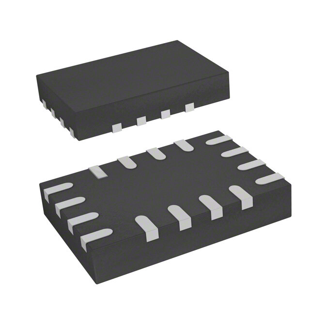
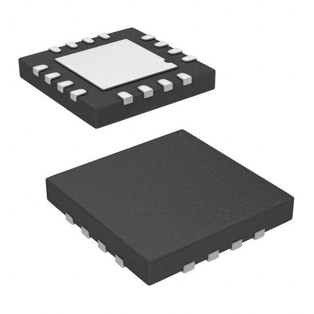
| 描述 | IC TOUCH SENSOR 1KEY SOT23-6电容触摸传感器 One-Channel Touch Sensor IC |
| 产品分类 | 电容式触摸传感器,接近传感器 IC电容触摸传感器 |
| 品牌 | Atmel |
| 产品手册 | |
| 产品图片 |
|
| rohs | 符合RoHS无铅 / 符合限制有害物质指令(RoHS)规范要求 |
| 产品系列 | Atmel AT42QT1010-TSHRQTouch™ |
| 数据手册 | |
| 产品型号 | AT42QT1010-TSHR |
| 产品种类 | 电容触摸传感器 |
| 供应商器件封装 | SOT-23-6 |
| 其它名称 | AT42QT1010-TSHR QS446DKR |
| 分辨率(位) | 9,14 b |
| 包装 | Digi-Reel® |
| 商标 | Atmel |
| 安装类型 | 表面贴装 |
| 封装/外壳 | SOT-23-6 |
| 工作温度 | -40°C ~ 85°C |
| 工厂包装数量 | 4500 |
| 数据接口 | 串行 |
| 数据速率/采样率(SPS,BPS) | - |
| 标准包装 | 1 |
| 电压-电源 | 1.8 V ~ 5.5 V |
| 电压基准 | 内部 |
| 电流-电源 | 729µA |
| 类型 | 电容式开关 |
| 触摸面板接口 | 2 线 |
| 评估工具 | 可供 |
| 输入/按键数 | 1 键 |


- 商务部:美国ITC正式对集成电路等产品启动337调查
- 曝三星4nm工艺存在良率问题 高通将骁龙8 Gen1或转产台积电
- 太阳诱电将投资9.5亿元在常州建新厂生产MLCC 预计2023年完工
- 英特尔发布欧洲新工厂建设计划 深化IDM 2.0 战略
- 台积电先进制程称霸业界 有大客户加持明年业绩稳了
- 达到5530亿美元!SIA预计今年全球半导体销售额将创下新高
- 英特尔拟将自动驾驶子公司Mobileye上市 估值或超500亿美元
- 三星加码芯片和SET,合并消费电子和移动部门,撤换高东真等 CEO
- 三星电子宣布重大人事变动 还合并消费电子和移动部门
- 海关总署:前11个月进口集成电路产品价值2.52万亿元 增长14.8%


PDF Datasheet 数据手册内容提取
AT42QT1010 AT42QT1010 Data Sheet Introduction The AT42QT1010 is a digital burst mode charge-transfer sensor that is capable of detecting near proximity or touch, making it ideal for implementing touch controls. The QT1010 is designed specifically for human interfaces like control panels, appliances, toys, lighting controls, or anywhere a mechanical switch or button may be found. It includes all hardware and signal processing functions necessary to provide stable sensing under a wide variety of changing conditions. Only a single low-cost capacitor is required for operation. Features • Number of Keys: – One – configurable as either a single key or a proximity sensor • Technology: – Patented spread-spectrum charge-transfer (direct mode) • Key outline sizes: – 6 mm × 6 mm or larger (panel thickness dependent); widely different sizes and shapes possible • Electrode design: – Solid or ring electrode shapes • PCB Layers required: – One • Electrode materials: – Etched copper, silver, carbon, Indium Tin Oxide (ITO) • Electrode substrates: – PCB, FPCB, plastic films, glass • Panel materials: – Plastic, glass, composites, painted surfaces (low particle density metallic paints possible) • Panel thickness: – Up to 12 mm glass, 6 mm plastic (electrode size and Cs dependent) • Key sensitivity: – Settable via capacitor (Cs) • Interface: – Digital output, active high • Moisture tolerance: – Increased moisture tolerance based on hardware design and firmware tuning • Operating Voltage: © 2017 Microchip Technology Inc. Datasheet DS40001946A-page 1
AT42QT1010 – 1.8 V – 5.5 V; 17 µA at 1.8 V typical • Package: – 6-pin SOT23-6 RoHS compliant – 8-pin UDFN/USON RoHS compliant • Signal processing: – Self-calibration, auto drift compensation, noise filtering • Applications: – Control panels, consumer appliances, proximity sensor applications, toys, lighting controls, mechanical switch or button, • Patents: – QTouch® technology (patented charge-transfer method) – HeartBeat (monitors health of device) © 2017 Microchip Technology Inc. Datasheet DS40001946A-page 2
Table of Contents Introduction......................................................................................................................1 Features..........................................................................................................................1 1. Pinout and Schematic................................................................................................5 1.1. Pinout Configurations...................................................................................................................5 1.2. Pin Descriptions...........................................................................................................................5 1.3. Schematics...................................................................................................................................6 2. Overview of the AT42QT1010...................................................................................8 2.1. Introduction...................................................................................................................................8 2.2. Basic Operation............................................................................................................................8 2.3. Electrode Drive.............................................................................................................................8 2.4. Sensitivity.....................................................................................................................................8 3. Operation Specifics.................................................................................................10 3.1. Run Modes.................................................................................................................................10 3.2. Threshold....................................................................................................................................11 3.3. Max On-duration.........................................................................................................................12 3.4. Detect Integrator.........................................................................................................................12 3.5. Forced Sensor Recalibration......................................................................................................12 3.6. Drift Compensation.....................................................................................................................12 3.7. Response Time..........................................................................................................................13 3.8. Spread Spectrum.......................................................................................................................13 3.9. Output Features.........................................................................................................................13 4. Circuit Guidelines....................................................................................................15 4.1. More Information........................................................................................................................15 4.2. Sample Capacitor.......................................................................................................................15 4.3. UDFN/USON Package Restrictions...........................................................................................15 4.4. Power Supply and PCB Layout..................................................................................................15 4.5. Power On...................................................................................................................................16 5. Specifications..........................................................................................................17 5.1. Absolute Maximum Specifications..............................................................................................17 5.2. Recommended Operating Conditions........................................................................................17 5.3. AC Specifications.......................................................................................................................17 5.4. Signal Processing.......................................................................................................................19 5.5. DC Specifications.......................................................................................................................20 5.6. Mechanical Dimensions.............................................................................................................21 5.7. Part Marking...............................................................................................................................23 5.8. Part Number...............................................................................................................................23 5.9. Moisture Sensitivity Level (MSL)................................................................................................24 6. Associated Documents............................................................................................25 © 2017 Microchip Technology Inc. Datasheet DS40001946A-page 3
AT42QT1010 7. Revision History.......................................................................................................26 The Microchip Web Site................................................................................................27 Customer Change Notification Service..........................................................................27 Customer Support.........................................................................................................27 Microchip Devices Code Protection Feature.................................................................27 Legal Notice...................................................................................................................28 Trademarks...................................................................................................................28 Quality Management System Certified by DNV.............................................................29 Worldwide Sales and Service........................................................................................30 © 2017 Microchip Technology Inc. Datasheet DS40001946A-page 4
AT42QT1010 1. Pinout and Schematic 1.1 Pinout Configurations 1.1.1 6-pin SOT23-6 Pin1ID SYNC/ OUT 1 6 MODE VSS 2 5 VDD SNSK 3 4 SNS 1.1.2 8-pin UDFN/USON Pin1ID SNSK 1 8 SNS N/C 2 7 VDD N/C 3 6 SYNC/MODE VSS 4 5 OUT 1.2 Pin Descriptions 1.2.1 6-pin SOT23-6 Table 1-1. Pin Listing Name Pin Type Comments If Unused, Connect To... OUT 1 O Output state — VSS 2 P Supply ground — SNSK 3 I/O Sense pin Cs + Key SNS 4 I/O Sense pin Cs VDD 5 P Power — SYNC 6 I SYNC and Mode Input Pin is either SYNC/Slow/Fast Mode, depending on logic level applied (see Section 3.1) © 2017 Microchip Technology Inc. Datasheet DS40001946A-page 5
AT42QT1010 Legend: I = Input only, O = Output only, push-pull, I/O = Input/output, OD = Open drain output, P = Ground or power 1.2.2 8-pin UDFN/USON Table 1-2. Pin Listing Name Pin Type Comments If Unused, Connect To... SNSK 1 I/O Sense pin Cs + Key N/C 2 — No connection — N/C 3 — No connection — VSS 4 P Supply ground — OUT 5 O Output state — SYNC/ 6 I SYNC and Mode Input Pin is either SYNC/Slow/Fast Mode, depending on logic MODE level applied (see Section 3.1) VDD 7 P Power — SNS 8 I/O Sense pin Cs Legend: I = Input only, O = Output only, push-pull, I/O = Input/output, OD = Open drain output, P = Ground or power 1.3 Schematics 1.3.1 6-pin SOT23-6 Figure 1-1. Basic Circuit Configuration VDD SENSE 5 ELECTRODE VDD 1 OUT SNSK 3 Rs Cs SNS 4 SYNC/MODE 6 Cx VSS 2 Note: A bypass capacitor should be tightly wired between Vdd and Vss and kept close to pin 5. © 2017 Microchip Technology Inc. Datasheet DS40001946A-page 6
AT42QT1010 1.3.2 8-pin UDFN/USON Figure 1-2. Basic Circuit Configuration Vdd SENSE 7 ELECTRODE VDD 5 OUT SNSK 1 Rs Cs 2 NC SNS 8 3 NC SYNC/MODE 6 Cx VSS 4 Note: A bypass capacitor should be tightly wired between Vdd and Vss and kept close to pin 5. © 2017 Microchip Technology Inc. Datasheet DS40001946A-page 7
AT42QT1010 2. Overview of the AT42QT1010 2.1 Introduction The AT42QT1010 is a digital burst mode charge-transfer sensor that is capable of detecting near- proximity or touch, making it ideal for implementing touch controls. With the proper electrode and circuit design, the self-contained digital IC will project a touch or proximity field to several centimeters through any dielectric like glass, plastic, stone, ceramic, and even most kinds of wood. It can also turn small metal-bearing objects into intrinsic sensors, making them responsive to proximity or touch. This capability, coupled with its ability to self-calibrate, can lead to entirely new product concepts. The QT1010 is designed specifically for human interfaces like control panels, appliances, toys, lighting controls, or anywhere a mechanical switch or button may be found. It includes all hardware and signal processing functions necessary to provide stable sensing under a wide variety of changing conditions. Only a single low-cost capacitor is required for operation. 2.2 Basic Operation Figure 1-1 and Figure 1-2 show basic circuits. The QT1010 employs bursts of charge-transfer cycles to acquire its signal. Burst mode permits power consumption in the microamp range, dramatically reduces RF emissions, lowers susceptibility to EMI, and yet permits excellent response time. Internally the signals are digitally processed to reject impulse noise, using a “consensus” filter which requires four consecutive confirmations of a detection before the output is activated. The QT switches and charge measurement hardware functions are all internal to the QT1010. 2.3 Electrode Drive For optimum noise immunity, the electrode should only be connected to SNSK. In all cases, the rule Cs >> Cx must be observed for proper operation; a typical load capacitance (Cx) ranges from 5–20 pF while Cs is usually about 2–50 nF. Increasing amounts of Cx destroy gain; therefore, it is important to limit the amount of stray capacitance on both SNS terminals. This can be done, for example, by minimizing trace lengths and widths, and keeping these traces away from power or ground traces or copper pours. The traces and any components associated with SNS and SNSK will become touch sensitive and should be treated with caution to limit the touch area to the desired location. A series resistor, Rs, should be placed in line with SNSK to the electrode to suppress ESD and EMC effects. 2.4 Sensitivity 2.4.1 Introduction The sensitivity on the QT1010 is a function of things like the value of Cs, electrode size and capacitance, electrode shape and orientation, the composition and aspect of the object to be sensed, the thickness © 2017 Microchip Technology Inc. Datasheet DS40001946A-page 8
AT42QT1010 and composition of any overlaying panel material, and the degree of ground coupling of both sensor and object. 2.4.2 Increasing Sensitivity In some cases it may be desirable to increase sensitivity; for example, when using the sensor with very thick panels having a low dielectric constant, or when the device is used as a proximity sensor. Sensitivity can often be increased by using a larger electrode or reducing panel thickness. Increasing electrode size can have diminishing returns, since high values of Cx will reduce sensor gain. The value of Cs also has a dramatic effect on sensitivity, and this can be increased in value with the trade-off of slower response time and more power. Increasing the electrode's surface area will not substantially increase touch sensitivity if its diameter is already much larger in surface area than the object being detected. Panel material can also be changed to one having a higher dielectric constant, which will better help to propagate the field. In the case of proximity detection, usually the object being detected is on an approaching hand, so a larger surface area can be effective. Ground planes around and under the electrode and its SNSK trace will cause high Cx loading and destroy gain. The possible signal-to-noise ratio benefits of ground area are more than negated by the decreased gain from the circuit so ground areas around electrodes are discouraged. Metal areas near the electrode will reduce the field strength and increase Cx loading and should be avoided, if possible. Keep ground away from the electrodes and traces. 2.4.3 Decreasing Sensitivity In some cases the QT1010 may be too sensitive. In this case gain can be easily lowered further by decreasing Cs. 2.4.4 Proximity Sensing By increasing the sensitivity, the QT1010 can be used as a very effective proximity sensor, allowing the presence of a nearby object (typically a hand) to be detected. In this scenario, as the object being sensed is typically a hand, very large electrode sizes can be used, which is extremely effective in increasing the sensitivity of the detector. In this case, the value of Cs will also need to be increased to ensure improved sensitivity, as mentioned in Section 2.4.2. Note that, although this affects the responsiveness of the sensor, it is less of an issue in proximity sensing applications; in such applications it is necessary to detect simply the presence of a large object, rather than a small, precise touch. © 2017 Microchip Technology Inc. Datasheet DS40001946A-page 9
AT42QT1010 3. Operation Specifics 3.1 Run Modes 3.1.1 Introduction The QT1010 has three running modes which depend on the state of the SYNC pin (high or low). 3.1.2 Fast Mode The QT1010 runs in Fast mode if the SYNC pin is permanently high. In this mode the QT1010 runs at maximum speed at the expense of increased current consumption. Fast mode is useful when speed of response is the prime design requirement. The delay between bursts in Fast mode is approximately 1 ms, as shown in the following figure. Figure 3-1. Fast Mode Bursts (SYNC Held High) SNSK ~1ms SYNC 3.1.3 Low Power Mode The QT1010 runs in Low Power (LP) mode if the SYNC pin is held low. In this mode it sleeps for approximately 80 ms at the end of each burst, saving power but slowing response. On detecting a possible key touch, it temporarily switches to Fast mode until either the key touch is confirmed or found to be spurious (via the detect integration process). It then returns to LP mode after the key touch is resolved, as shown in the following figure. Figure 3-2. Low Power Mode (SYNC Held Low) h fast detect ey uc 80 ms K o integrator t sleep sleep sleep SNSK SYNC OUT 3.1.4 SYNC Mode It is possible to synchronize the device to an external clock source by placing an appropriate waveform on the SYNC pin. SYNC mode can synchronize multiple QT1010 devices to each other to prevent cross- © 2017 Microchip Technology Inc. Datasheet DS40001946A-page 10
AT42QT1010 interference, or it can be used to enhance noise immunity from low frequency sources such as 50Hz or 60Hz mains signals. The SYNC pin is sampled at the end of each burst. If the device is in Fast mode and the SYNC pin is sampled high, then the device continues to operate in Fast mode (Figure 3-1). If SYNC is sampled low, then the device goes to sleep. From then on, it will operate in SYNC mode (Figure 3-2). Therefore, to guarantee entry into SYNC mode, the low period of the SYNC signal should be longer than the burst length (Figure 3-3). Figure 3-3. SYNC Mode (Triggered by SYNC Edges) SNSK sleep sleep sleep ReverttoFastMode SYNC slowmodesleepperiod SNSK sleep sleep sleep ReverttoSlowMode slowmodesleepperiod SYNC However, once SYNC mode has been entered, if the SYNC signal consists of a series of short pulses (>10 μs), then a burst will only occur on the falling edge of each pulse (Figure 3-4) instead of on each change of SYNC signal, as normal (Figure 3-3). In SYNC mode, the device will sleep after each measurement burst (just as in LP mode) but will be awakened by a change in the SYNC signal in either direction, resulting in a new measurement burst. If SYNC remains unchanged for a period longer than the LP mode sleep period (about 80 ms), the device will resume operation in either Fast or LP mode depending on the level of the SYNC pin (Figure 3-3). There is no Detect Integrator (DI) in SYNC mode (each touch is a detection), but the Max On-duration will depend on the time between SYNC pulses, refer toMax On-duration and Section 3.4. Recalibration timeout is a fixed number of measurements so it will vary with the SYNC period. Figure 3-4. SYNC Mode (Short Pulses) SNSK >10μs >10μs >10μs SYNC 3.2 Threshold The internal signal threshold level is fixed at 10 counts of change with respect to the internal reference level, which in turn adjusts itself slowly in accordance with the drift compensation mechanism. The QT1010 employs a hysteresis dropout of two counts of the delta between the reference and threshold levels. © 2017 Microchip Technology Inc. Datasheet DS40001946A-page 11
AT42QT1010 3.3 Max On-duration If an object or material obstructs the sense pad, the signal may rise enough to create a detection, preventing further operation. To prevent this, the sensor includes a timer which monitors detections. If a detection exceeds the timer setting, the sensor performs a full recalibration. This is known as the Max On-duration feature and is set to ~60s (at 3V in LP mode). This will vary slightly with Cs and if SYNC mode is used. As the internal timebase for Max On-duration is determined by the burst rate, the use of SYNC can cause dramatic changes in this parameter depending on the SYNC pulse spacing. For example, at 60Hz SYNC mode the Max On-duration will be ~6s at 3V. 3.4 Detect Integrator It is desirable to suppress detections generated by electrical noise or from quick brushes with an object. To accomplish this, the QT1010 incorporates a Detect Integration (DI) counter that increments with each detection until a limit is reached, after which the output is activated. If no detection is sensed prior to the final count, the counter is reset immediately to zero. In the QT1010, the required count is four. In LP mode the device will switch to Fast mode temporarily in order to resolve the detection more quickly; after a touch is either confirmed or denied, the device will revert back to normal LP mode operation automatically. The DI can also be viewed as a “consensus filter” that requires four successive detections to create an output. 3.5 Forced Sensor Recalibration The QT1010 has no recalibration pin; a forced recalibration is accomplished when the device is powered up or after the recalibration timeout. However, supply drain is low so it is a simple matter to treat the entire IC as a controllable load; driving the QT1010's Vdd pin directly from another logic gate or a microcontroller port will serve as both power and “forced recalibration”. The source resistance of most CMOS gates and microcontrollers is low enough to provide direct power without problem. 3.6 Drift Compensation Signal drift can occur because of changes in Cx and Cs over time. It is crucial that drift be compensated for; otherwise, false detections, non-detections, and sensitivity shifts will follow. Drift compensation (Figure 3-5) is performed by making the reference level track the raw signal at a slow rate, but only while there is no detection in effect. The rate of adjustment must be performed slowly, otherwise legitimate detections could be ignored. The QT1010 drift compensates using a slew-rate limited change to the reference level; the threshold and hysteresis values are slaved to this reference. Once an object is sensed, the drift compensation mechanism ceases since the signal is legitimately high, and therefore should not cause the reference level to change. © 2017 Microchip Technology Inc. Datasheet DS40001946A-page 12
AT42QT1010 Figure 3-5. Drift Compensation Signal Hysteresis Threshold Reference Output The QT1010 drift compensation is asymmetric; the reference level drift-compensates in one direction faster than it does in the other. Specifically, it compensates faster for decreasing signals than for increasing signals. Increasing signals should not be compensated for quickly, since an approaching finger could be compensated for partially or entirely before even approaching the sense electrode. However, an obstruction over the sense pad, for which the sensor has already made full allowance, could suddenly be removed leaving the sensor with an artificially elevated reference level and thus become insensitive to touch. In this latter case, the sensor will compensate for the object's removal very quickly, usually in only a few seconds. With large values of Cs and small values of Cx, drift compensation will appear to operate more slowly than with the converse. Note that the positive and negative drift compensation rates are different. 3.7 Response Time The QT1010's response time is highly dependent on run mode and burst length, which in turn is dependent on Cs and Cx. With increasing Cs, response time slows, while increasing levels of Cx reduce response time. The response time will also be a lot slower in LP or SYNC mode due to a longer time between burst measurements. 3.8 Spread Spectrum The QT1010 modulates its internal oscillator by ±7.5% during the measurement burst. This spreads the generated noise over a wider band, reducing emission levels. This also reduces susceptibility since there is no longer a single fundamental burst frequency. 3.9 Output Features 3.9.1 Output The output of the QT1010 is active-high upon detection. The output will remain active-high for the duration of the detection, or until the Max On-duration expires, whichever occurs first. If a Max On-duration timeout occurs first, the sensor performs a full recalibration and the output becomes inactive (low) until the next detection. 3.9.2 HeartBeat Output The QT1010 output has a HeartBeat “health” indicator superimposed on it in all modes. This operates by taking the output pin into a three-state mode for 15 μs, once before every QT burst. This output state can be used to determine that the sensor is operating properly, using one of several simple methods, or it can be ignored. © 2017 Microchip Technology Inc. Datasheet DS40001946A-page 13
AT42QT1010 The HeartBeat indicator can be sampled by using a pull-up resistor on the OUT pin (Figure 3-6), and feeding the resulting positive-going pulse into a counter, flip flop, one-shot, or other circuit. The pulses will only be visible when the chip is not detecting a touch. Figure 3-6. Obtaining HeartBeat Pulses with a Pull-up Resistor (SOT23-6) VDD 5 VDD HeartBeat" Pulse Ro 1 OUT SNSK 3 SNS 4 SYNC/MODE 6 VSS 2 If the sensor is wired to a microcontroller as shown in Figure 3-7, the microcontroller can reconfigure the load resistor to either Vss or Vdd depending on the output state of the QT1010, so that the pulses are evident in either state. Figure 3-7. Using a Microcontroller to Obtain HeartBeat Pulses in Either Output State (SOT23-6) Port_M.x Ro 1 OUT SNSK 3 Microcontroller SNS 4 Port_M.y 6 SYNC/MODE Electromechanical devices like relays will usually ignore the short HeartBeat pulse. The pulse also has too low a duty cycle to visibly affect LEDs. It can be filtered completely if desired, by adding an RC filter to the output, or if interfacing directly and only to a high-impedance CMOS input, by doing nothing or at most adding a small noncritical capacitor from OUT to Vss. 3.9.3 Output Drive The OUT pin is active high and can sink or source up to 2 mA. When a large value of Cs (>20 nF) is used, the OUT current should be limited to <1 mA to prevent gain-shifting side effects, which happen when the load current creates voltage drops on the die and bonding wires; these small shifts can materially influence the signal level to cause detection instability. © 2017 Microchip Technology Inc. Datasheet DS40001946A-page 14
AT42QT1010 4. Circuit Guidelines 4.1 More Information Refer to Application Note QTAN0002, "Secrets of a Successful QTouch® Design", and the "Touch Sensors Design Guide" (both downloadable from http://www.microchip.com), for more information on construction and design methods. 4.2 Sample Capacitor Cs is the charge sensing sample capacitor. The required Cs value depends on the thickness of the panel and its dielectric constant. Thicker panels require larger values of Cs. Typical values are 2 nF to 50 nF depending on the sensitivity required; larger values of Cs demand higher stability and better dielectric to ensure reliable sensing. The Cs capacitor should be a stable type, such as X7R ceramic or PPS film. For more consistent sensing from unit to unit, 5% tolerance capacitors are recommended. X7R ceramic types can be obtained in 5% tolerance at little or no extra cost. In applications where high sensitivity (long burst length) is required, the use of PPS capacitors is recommended. For battery powered operation, a higher value sample capacitor is recommended (typical value 8.2 nF). 4.3 UDFN/USON Package Restrictions The central pad on the underside of the UDFN/USON chip is connected to ground. Do not run any tracks underneath the body of the chip, only ground. 4.4 Power Supply and PCB Layout See Section 5.2 for the power supply range. At 3V, current drain averages less than 500 μA in Fast mode. If the power supply is shared with another electronic system, care should be taken to ensure that the supply is free of digital spikes, sags, and surges which can adversely affect the QT1010. The QT1010 will track slow changes in Vdd, but it can be badly affected by rapid voltage fluctuations. It is highly recommended that a separate voltage regulator be used just for the QT1010 to isolate it from power supply shifts caused by other components. If desired, the supply can be regulated using a Low Dropout (LDO) regulator, although such regulators often have poor transient line and load stability. See Application Note QTAN0002, "Secrets of a Successful QTouch® Design" for further information. Parts placement: The chip should be placed to minimize the SNSK trace length to reduce low frequency pickup, and to reduce stray Cx, which degrades gain. The Cs and Rs resistors (see Figure 1-1) should be placed as close to the body of the chip as possible so that the trace between Rs and the SNSK pin is very short, thereby reducing the antenna-like ability of this trace to pick up high frequency signals and feed them directly into the chip. A ground plane can be used under the chip and the associated discrete components, but the trace from the Rs resistor and the electrode should not run near ground to reduce loading. For best EMC performance, the circuit should be made entirely with SMT components. © 2017 Microchip Technology Inc. Datasheet DS40001946A-page 15
AT42QT1010 Electrode trace routing: Keep the electrode trace (and the electrode itself) away from other signal, power, and ground traces including over or next to ground planes. Adjacent switching signals can induce noise onto the sensing signal; any adjacent trace or ground plane next to, or under, the electrode trace will cause an increase in Cx load and desensitize the device. Note: For proper operation, a 100 nF (0.1 μF) ceramic bypass capacitor must be used directly between Vdd and Vss to prevent latch-up if there are substantial Vdd transients; for example, during an ESD event. The bypass capacitor should be placed very close to the Vss and Vdd pins. 4.5 Power On On initial power up, the QT1010 requires approximately 100 ms to power on to allow power supplies to stabilize. During this time the OUT pin state is not valid and should be ignored. © 2017 Microchip Technology Inc. Datasheet DS40001946A-page 16
AT42QT1010 5. Specifications 5.1 Absolute Maximum Specifications Operating temperature –40°C to +85°C Storage temperature –55°C to +125°C Vdd 0 to +6.5 V Max continuous pin current, any control or drive pin ±20 mA Short circuit duration to Vss, any pin Infinite Short circuit duration to Vdd, any pin Infinite Voltage forced onto any pin –0.6V to (Vdd + 0.6) V CAUTION: Stresses beyond those listed under Absolute Maximum Specifications may cause permanent damage to the device. This is a stress rating only and functional operation of the device at these or other conditions beyond those indicated in the operational sections of this specification is not implied. Exposure to absolute maximum specification conditions for extended periods may affect device reliability. 5.2 Recommended Operating Conditions Vdd +1.8 to 5.5 V Short-term supply ripple + noise ±20 mV Long-term supply stability ±100 mV Cs value 2 to 50 nF Cx value 5 to 50 pF 5.3 AC Specifications Table 5-1. Vdd = 3.0 V, Cs = 4.7 nF, Cx = 5 pF, Ta = recommended range, unless otherwise noted Parameter Description Min Typ Max Units Notes Trc Recalibration time – 200 – ms Cs, Cx dependent Tpc Charge duration – 3.05 – μs ±7.5% spread spectrum variation Tpt Transfer duration – 9.0 – μs ±7.5% spread spectrum variation Tg1 Time between end of burst and – 1.2 – ms start of the next (Fast mode) © 2017 Microchip Technology Inc. Datasheet DS40001946A-page 17
AT42QT1010 Parameter Description Min Typ Max Units Notes Tg2 Time between end of burst and – 80 – ms Increases with decreasing start of the next (LP mode) Vdd See Figure 5-1 Tbl Burst length – 2.45 – ms Vdd, Cs and Cx dependent. See Section 4.2 for capacitor selection. Tr Response time – – 100 ms Thb HeartBeat pulse width – 15 – μs Figure 5-1. Tg2 Time Between Bursts (LP Mode) © 2017 Microchip Technology Inc. Datasheet DS40001946A-page 18
AT42QT1010 Figure 5-2. Tbl Burst Length 5.4 Signal Processing Table 5-2. Vdd = 3.0V, Cs = 4.7 nF, Cx = 5 pF, Ta = recommended range, unless otherwise noted Description Min Typ Max Units Notes Threshold differential 10 counts Hysteresis 2 counts Consensus filter length 4 samples Max on-duration 60 seconds (At 3 V in LP mode) Will vary in SYNC mode and with Vdd © 2017 Microchip Technology Inc. Datasheet DS40001946A-page 19
AT42QT1010 5.5 DC Specifications Table 5-3. Vdd = 3.0V, Cs = 4.7 nF, Cx = 5 pF, Ta = recommended range, unless otherwise noted Parameter Description Min Typ Max Units Notes Vdd Supply voltage 1.8 5.5 V Idd Supply current, Fast – 203.0 – μA 1.8 V mode 246.0 2.0 V 378.5 3.0 V 542.5 4.0 V 729.0 5.0 V IddI Supply current, LP mode – 16.5 – μA 1.8 V 19.5 2.0 V 34.0 3.0 V 51.5 4.0 V 73.5 5.0 V Vdds Supply turn-on slope 10 – – V/s Required for proper start-up Vil Low input logic level – – 0.2 × Vdd V Vdd = 1.8 V – 2.4 V 0.3 × Vdd Vdd = 2.4 V – 5.5 V Vhl High input logic level 0.7 × Vdd – – V Vdd = 1.8 V – 2.4 V 0.6 × Vdd Vdd = 2.4 V – 5.5 V Vol Low output voltage – – 0.5 V OUT, 4 mA sink Voh High output voltage 2.3 – – V OUT, 1 mA source Iil Input leakage current – <0.05 1 μA Cx Load capacitance range 2 – 50 pF Ar Acquisition resolution – 9 14 bits © 2017 Microchip Technology Inc. Datasheet DS40001946A-page 20
AT42QT1010 5.6 Mechanical Dimensions 5.6.1 6-pin SOT23-6 D 6 5 4 A E E1 A2 A Pin #1 ID 0.10 C SEATING PLANE A 1 2 3 A1 C Side View b e Top View A2 A 0.10 C SEATING PLANE c 0.25 A1 C SEATING PLANE View A-A O C SEE VIEW B L View B COMMON DIMENSIONS (Unit of Measure = mm) SYMBOL MIN NOM MAX NOTE A – – 1.45 A1 0 – 0.15 A2 0.90 – 1.30 D 2.80 2.90 3.00 2 Notes: 1. This package is compliant with JEDEC specification E 2.60 2.80 3.00 MO-178 Variation AB. 2. Dimension D does not include mold Flash, protrusions or E1 1.50 1.60 1.75 gate burrs. Mold Flash, protrustion or gate burrs shall not L 0.30 0.45 0.55 exceed 0.25 mm per end. 3. Dimension b does not include dambar protrusion. e 0.95 BSC Allowable dambar protrusion shall not cause the lead width b 0.30 – 0.50 3 to exceed the maximum b dimension by more than 0.08 mm 4. Die is facing down after trim/form. c 0.09 – 0.20 q 0° – 8° 1/25/13 TITLE GPC DRAWING NO. REV. Package Drawing Contact: 6ST1, 6-lead, 2.90 x 1.60 mm Plastic Small Outline TAQ 6ST1 B Package (SOT23) packagedrawings@atmel.com Note: For the most current package drawings, please see the Microchip Packaging Specification located at http://www.microchip.com/packaging © 2017 Microchip Technology Inc. Datasheet DS40001946A-page 21
AT42QT1010 5.6.2 8-pin UDFN/USON Bottom view Top view Side view D2 A e 8 7 6 5 5 8 k C0.2 E E2 PIN 1 ID L 1 2 3 4 4 b 1 D A1 f 0.05C A 8X d 0.05C COMMON DIMENSIONS C Side view A1 (Unit of Measure = mm) SYMBOL MIN NOM MAX NOTE A - - 0.60 A1 0.00 - 0.05 b 0.20 - 0.30 NOTES: D 1.95 2.00 2.05 1. All dimensions are in mm. Angles in degrees. D2 1.40 1.50 1.60 2. Coplanarity applies to the exposed pad as well as the terminals. Coplanarity shall not exceed 0.05 mm. E 1.95 2.00 2.05 3. Warpage shall not exceed 0.05 mm. E2 0.80 0.90 1.00 4. Refer to JEDEC MO-236/MO-252. e 0.50 BSC L 0.20 0.30 0.40 k 0.20 - - 01/25/13 TITLE GPC DRAWING NO. REV. 8MA4, 8-pad, 2.0x2.0x0.6 mm Body, 0.5 mm pitch, Package Drawing Contact: 0.9x1.5 mm Exposed ePad, Ultra-Thin Dual Flat YAG 8MA4 B packagedrawings@atmel.com No Lead Package (UDFN/USON) Note: For the most current package drawings, please see the Microchip Packaging Specification located at http://www.microchip.com/packaging © 2017 Microchip Technology Inc. Datasheet DS40001946A-page 22
AT42QT1010 5.7 Part Marking 5.7.1 AT42QT1010– 6-pin SOT23-6 1010 Abbreviated PartNumber: Pin1ID AT42QT1010 Note: Samples of the AT42QT1010 may also be marked T10E. 5.7.2 AT42QT1010 – 8-pin UDFN/USON Abbreviated PartNumber: 1010 1010 AT42QT DieRevision (Example:“E” shown) Classcode (H=Industrial, HEC greenNiPdAu) AssemblyLocation Code (Example:“C”shown) YZZ Pin1ID LotNumberTrace code(Variabletext) Pin1 LastDigitofYear (Variabletext) Note: Samples of the AT42QT1010 may also be marked T10 5.8 Part Number Part Number Description AT42QT1010(1) 6-pin SOT23 RoHS compliant IC AT42QT1010-TSHR 6-pin SOT23 RoHS compliant IC AT42QT1010-MAH 8-pin UDFN/USON RoHS compliant IC Notes: 1. Marking details: Top mark 1st line: ddddTY Top mark 2nd line: wwxxx dddd= device, special code T= Type Y= Year last digit ww= calendar workweek xxx = trace code © 2017 Microchip Technology Inc. Datasheet DS40001946A-page 23
AT42QT1010 5.9 Moisture Sensitivity Level (MSL) MSL Rating Peak Body Temperature Specifications MSL1 260oC IPC/JEDEC J-STD-020 © 2017 Microchip Technology Inc. Datasheet DS40001946A-page 24
AT42QT1010 6. Associated Documents For additional information, refer to the following document (downloadable from the Touch Technology area of the Microchip website, www.microchip.com): • Touch Sensors Design Guide • QTAN0002 – Secrets of a Successful QTouch® Design © 2017 Microchip Technology Inc. Datasheet DS40001946A-page 25
AT42QT1010 7. Revision History Revision No. History Revision A – May 2009 Initial release Revision B – August 2009 Update for chip revision 2.2 Revision C – August 2009 Minor update for clarity Revision D – January 2010 Power specifications updated for revision 2.4.1 Revision E – January 2010 Part markings updated Revision F – February 2010 MSL specification revised Other minor updates Revision G – March 2010 Update for chip revision 2.6 • Migration advice added Revision H – May 2010 UDFN/USON package added Revision I – May 2013 Applied new template DS40001946A – August 2017 Part marking clarification added. Replaces Atmel document 9541I. © 2017 Microchip Technology Inc. Datasheet DS40001946A-page 26
AT42QT1010 The Microchip Web Site Microchip provides online support via our web site at http://www.microchip.com/. This web site is used as a means to make files and information easily available to customers. Accessible by using your favorite Internet browser, the web site contains the following information: • Product Support – Data sheets and errata, application notes and sample programs, design resources, user’s guides and hardware support documents, latest software releases and archived software • General Technical Support – Frequently Asked Questions (FAQ), technical support requests, online discussion groups, Microchip consultant program member listing • Business of Microchip – Product selector and ordering guides, latest Microchip press releases, listing of seminars and events, listings of Microchip sales offices, distributors and factory representatives Customer Change Notification Service Microchip’s customer notification service helps keep customers current on Microchip products. Subscribers will receive e-mail notification whenever there are changes, updates, revisions or errata related to a specified product family or development tool of interest. To register, access the Microchip web site at http://www.microchip.com/. Under “Support”, click on “Customer Change Notification” and follow the registration instructions. Customer Support Users of Microchip products can receive assistance through several channels: • Distributor or Representative • Local Sales Office • Field Application Engineer (FAE) • Technical Support Customers should contact their distributor, representative or Field Application Engineer (FAE) for support. Local sales offices are also available to help customers. A listing of sales offices and locations is included in the back of this document. Technical support is available through the web site at: http://www.microchip.com/support Microchip Devices Code Protection Feature Note the following details of the code protection feature on Microchip devices: • Microchip products meet the specification contained in their particular Microchip Data Sheet. • Microchip believes that its family of products is one of the most secure families of its kind on the market today, when used in the intended manner and under normal conditions. • There are dishonest and possibly illegal methods used to breach the code protection feature. All of these methods, to our knowledge, require using the Microchip products in a manner outside the operating specifications contained in Microchip’s Data Sheets. Most likely, the person doing so is engaged in theft of intellectual property. • Microchip is willing to work with the customer who is concerned about the integrity of their code. © 2017 Microchip Technology Inc. Datasheet DS40001946A-page 27
AT42QT1010 • Neither Microchip nor any other semiconductor manufacturer can guarantee the security of their code. Code protection does not mean that we are guaranteeing the product as “unbreakable.” Code protection is constantly evolving. We at Microchip are committed to continuously improving the code protection features of our products. Attempts to break Microchip’s code protection feature may be a violation of the Digital Millennium Copyright Act. If such acts allow unauthorized access to your software or other copyrighted work, you may have a right to sue for relief under that Act. Legal Notice Information contained in this publication regarding device applications and the like is provided only for your convenience and may be superseded by updates. It is your responsibility to ensure that your application meets with your specifications. MICROCHIP MAKES NO REPRESENTATIONS OR WARRANTIES OF ANY KIND WHETHER EXPRESS OR IMPLIED, WRITTEN OR ORAL, STATUTORY OR OTHERWISE, RELATED TO THE INFORMATION, INCLUDING BUT NOT LIMITED TO ITS CONDITION, QUALITY, PERFORMANCE, MERCHANTABILITY OR FITNESS FOR PURPOSE. Microchip disclaims all liability arising from this information and its use. Use of Microchip devices in life support and/or safety applications is entirely at the buyer’s risk, and the buyer agrees to defend, indemnify and hold harmless Microchip from any and all damages, claims, suits, or expenses resulting from such use. No licenses are conveyed, implicitly or otherwise, under any Microchip intellectual property rights unless otherwise stated. Trademarks The Microchip name and logo, the Microchip logo, AnyRate, AVR, AVR logo, AVR Freaks, BeaconThings, BitCloud, CryptoMemory, CryptoRF, dsPIC, FlashFlex, flexPWR, Heldo, JukeBlox, KeeLoq, KeeLoq logo, Kleer, LANCheck, LINK MD, maXStylus, maXTouch, MediaLB, megaAVR, MOST, MOST logo, MPLAB, OptoLyzer, PIC, picoPower, PICSTART, PIC32 logo, Prochip Designer, QTouch, RightTouch, SAM-BA, SpyNIC, SST, SST Logo, SuperFlash, tinyAVR, UNI/O, and XMEGA are registered trademarks of Microchip Technology Incorporated in the U.S.A. and other countries. ClockWorks, The Embedded Control Solutions Company, EtherSynch, Hyper Speed Control, HyperLight Load, IntelliMOS, mTouch, Precision Edge, and Quiet-Wire are registered trademarks of Microchip Technology Incorporated in the U.S.A. Adjacent Key Suppression, AKS, Analog-for-the-Digital Age, Any Capacitor, AnyIn, AnyOut, BodyCom, chipKIT, chipKIT logo, CodeGuard, CryptoAuthentication, CryptoCompanion, CryptoController, dsPICDEM, dsPICDEM.net, Dynamic Average Matching, DAM, ECAN, EtherGREEN, In-Circuit Serial Programming, ICSP, Inter-Chip Connectivity, JitterBlocker, KleerNet, KleerNet logo, Mindi, MiWi, motorBench, MPASM, MPF, MPLAB Certified logo, MPLIB, MPLINK, MultiTRAK, NetDetach, Omniscient Code Generation, PICDEM, PICDEM.net, PICkit, PICtail, PureSilicon, QMatrix, RightTouch logo, REAL ICE, Ripple Blocker, SAM-ICE, Serial Quad I/O, SMART-I.S., SQI, SuperSwitcher, SuperSwitcher II, Total Endurance, TSHARC, USBCheck, VariSense, ViewSpan, WiperLock, Wireless DNA, and ZENA are trademarks of Microchip Technology Incorporated in the U.S.A. and other countries. SQTP is a service mark of Microchip Technology Incorporated in the U.S.A. Silicon Storage Technology is a registered trademark of Microchip Technology Inc. in other countries. GestIC is a registered trademark of Microchip Technology Germany II GmbH & Co. KG, a subsidiary of Microchip Technology Inc., in other countries. All other trademarks mentioned herein are property of their respective companies. © 2017, Microchip Technology Incorporated, Printed in the U.S.A., All Rights Reserved. © 2017 Microchip Technology Inc. Datasheet DS40001946A-page 28
AT42QT1010 ISBN: 978-1-5224-2069-9 Quality Management System Certified by DNV ISO/TS 16949 Microchip received ISO/TS-16949:2009 certification for its worldwide headquarters, design and wafer fabrication facilities in Chandler and Tempe, Arizona; Gresham, Oregon and design centers in California and India. The Company’s quality system processes and procedures are for its PIC® MCUs and dsPIC® DSCs, KEELOQ® code hopping devices, Serial EEPROMs, microperipherals, nonvolatile memory and analog products. In addition, Microchip’s quality system for the design and manufacture of development systems is ISO 9001:2000 certified. © 2017 Microchip Technology Inc. Datasheet DS40001946A-page 29
Worldwide Sales and Service AMERICAS ASIA/PACIFIC ASIA/PACIFIC EUROPE Corporate Office Asia Pacific Office China - Xiamen Austria - Wels 2355 West Chandler Blvd. Suites 3707-14, 37th Floor Tel: 86-592-2388138 Tel: 43-7242-2244-39 Chandler, AZ 85224-6199 Tower 6, The Gateway Fax: 86-592-2388130 Fax: 43-7242-2244-393 Tel: 480-792-7200 Harbour City, Kowloon China - Zhuhai Denmark - Copenhagen Fax: 480-792-7277 Hong Kong Tel: 86-756-3210040 Tel: 45-4450-2828 Technical Support: Tel: 852-2943-5100 Fax: 86-756-3210049 Fax: 45-4485-2829 http://www.microchip.com/ Fax: 852-2401-3431 India - Bangalore Finland - Espoo support Australia - Sydney Tel: 91-80-3090-4444 Tel: 358-9-4520-820 Web Address: Tel: 61-2-9868-6733 Fax: 91-80-3090-4123 France - Paris www.microchip.com Fax: 61-2-9868-6755 India - New Delhi Tel: 33-1-69-53-63-20 Atlanta China - Beijing Tel: 91-11-4160-8631 Fax: 33-1-69-30-90-79 Duluth, GA Tel: 86-10-8569-7000 Fax: 91-11-4160-8632 France - Saint Cloud Tel: 678-957-9614 Fax: 86-10-8528-2104 India - Pune Tel: 33-1-30-60-70-00 Fax: 678-957-1455 China - Chengdu Tel: 91-20-3019-1500 Germany - Garching Austin, TX Tel: 86-28-8665-5511 Japan - Osaka Tel: 49-8931-9700 Tel: 512-257-3370 Fax: 86-28-8665-7889 Tel: 81-6-6152-7160 Germany - Haan Boston China - Chongqing Fax: 81-6-6152-9310 Tel: 49-2129-3766400 Westborough, MA Tel: 86-23-8980-9588 Japan - Tokyo Germany - Heilbronn Tel: 774-760-0087 Fax: 86-23-8980-9500 Tel: 81-3-6880- 3770 Tel: 49-7131-67-3636 Fax: 774-760-0088 China - Dongguan Fax: 81-3-6880-3771 Germany - Karlsruhe Chicago Tel: 86-769-8702-9880 Korea - Daegu Tel: 49-721-625370 Itasca, IL China - Guangzhou Tel: 82-53-744-4301 Germany - Munich Tel: 630-285-0071 Tel: 86-20-8755-8029 Fax: 82-53-744-4302 Tel: 49-89-627-144-0 Fax: 630-285-0075 China - Hangzhou Korea - Seoul Fax: 49-89-627-144-44 Dallas Tel: 86-571-8792-8115 Tel: 82-2-554-7200 Germany - Rosenheim Addison, TX Fax: 86-571-8792-8116 Fax: 82-2-558-5932 or Tel: 49-8031-354-560 Tel: 972-818-7423 China - Hong Kong SAR 82-2-558-5934 Israel - Ra’anana Fax: 972-818-2924 Tel: 852-2943-5100 Malaysia - Kuala Lumpur Tel: 972-9-744-7705 Detroit Fax: 852-2401-3431 Tel: 60-3-6201-9857 Italy - Milan Novi, MI China - Nanjing Fax: 60-3-6201-9859 Tel: 39-0331-742611 Tel: 248-848-4000 Tel: 86-25-8473-2460 Malaysia - Penang Fax: 39-0331-466781 Houston, TX Fax: 86-25-8473-2470 Tel: 60-4-227-8870 Italy - Padova Tel: 281-894-5983 China - Qingdao Fax: 60-4-227-4068 Tel: 39-049-7625286 Indianapolis Tel: 86-532-8502-7355 Philippines - Manila Netherlands - Drunen Noblesville, IN Fax: 86-532-8502-7205 Tel: 63-2-634-9065 Tel: 31-416-690399 Tel: 317-773-8323 China - Shanghai Fax: 63-2-634-9069 Fax: 31-416-690340 Fax: 317-773-5453 Tel: 86-21-3326-8000 Singapore Norway - Trondheim Tel: 317-536-2380 Fax: 86-21-3326-8021 Tel: 65-6334-8870 Tel: 47-7289-7561 Los Angeles China - Shenyang Fax: 65-6334-8850 Poland - Warsaw Mission Viejo, CA Tel: 86-24-2334-2829 Taiwan - Hsin Chu Tel: 48-22-3325737 Tel: 949-462-9523 Fax: 86-24-2334-2393 Tel: 886-3-5778-366 Romania - Bucharest Fax: 949-462-9608 China - Shenzhen Fax: 886-3-5770-955 Tel: 40-21-407-87-50 Tel: 951-273-7800 Tel: 86-755-8864-2200 Taiwan - Kaohsiung Spain - Madrid Raleigh, NC Fax: 86-755-8203-1760 Tel: 886-7-213-7830 Tel: 34-91-708-08-90 Tel: 919-844-7510 China - Wuhan Taiwan - Taipei Fax: 34-91-708-08-91 New York, NY Tel: 86-27-5980-5300 Tel: 886-2-2508-8600 Sweden - Gothenberg Tel: 631-435-6000 Fax: 86-27-5980-5118 Fax: 886-2-2508-0102 Tel: 46-31-704-60-40 San Jose, CA China - Xian Thailand - Bangkok Sweden - Stockholm Tel: 408-735-9110 Tel: 86-29-8833-7252 Tel: 66-2-694-1351 Tel: 46-8-5090-4654 Tel: 408-436-4270 Fax: 86-29-8833-7256 Fax: 66-2-694-1350 UK - Wokingham Canada - Toronto Tel: 44-118-921-5800 Tel: 905-695-1980 Fax: 44-118-921-5820 Fax: 905-695-2078 © 2017 Microchip Technology Inc. Datasheet DS40001946A-page 30
Mouser Electronics Authorized Distributor Click to View Pricing, Inventory, Delivery & Lifecycle Information: M icrochip: AT42QT1010-MAH AT42QT1010-TSHR AT42QT1010-MAHR