ICGOO在线商城 > 集成电路(IC) > 接口 - 传感器,电容式触摸 > QT60168-ASG
/QT60168-ASG.jpg)
 Datasheet下载
- 型号: QT60168-ASG
- 制造商: Atmel
- 库位|库存: xxxx|xxxx
- 要求:
| 数量阶梯 | 香港交货 | 国内含税 |
| +xxxx | $xxxx | ¥xxxx |
查看当月历史价格
查看今年历史价格
QT60168-ASG产品简介:
ICGOO电子元器件商城为您提供QT60168-ASG由Atmel设计生产,在icgoo商城现货销售,并且可以通过原厂、代理商等渠道进行代购。 QT60168-ASG价格参考。AtmelQT60168-ASG封装/规格:接口 - 传感器,电容式触摸, Capacitive Touch Buttons 32-TQFP (7x7)。您可以下载QT60168-ASG参考资料、Datasheet数据手册功能说明书,资料中有QT60168-ASG 详细功能的应用电路图电压和使用方法及教程。
Microchip Technology的QT60168-ASG是一款电容式触摸传感器接口芯片,广泛应用于需要高灵敏度和可靠性的触控场景。以下是其主要应用场景:

1. 家用电器:
   QT60168-ASG可用于洗衣机、冰箱、微波炉、烤箱等家电的触摸控制面板,替代传统机械按键,提供更现代、简洁的用户界面。

2. 消费电子设备:
   适用于多媒体播放器、遥控器、音响设备等,实现音量调节、电源开关等功能的触控操作,提升用户体验。

3. 工业控制:
   在工业设备中用作人机交互界面,例如触摸式控制面板或按钮,用于调节参数、启动/停止设备等操作。

4. 智能家居:
   用于智能灯控开关、温控器、安防设备等,支持多种触控模式(如滑动条、按钮),增强智能家居产品的交互性。

5. 医疗设备:
   应用于便携式医疗设备(如血压计、血糖仪)或大型医疗仪器的触摸控制面板,提供防水、防尘性能,确保在复杂环境下的可靠性。

6. 汽车电子:
   适合车内触控应用,如空调控制面板、音频系统调节等,具备抗干扰能力强的特点,适应汽车环境的特殊需求。

7. 游戏与娱乐设备:
   用于游戏控制器、互动玩具等,提供灵敏的触控反馈,增强互动体验。

QT60168-ASG支持多达16个独立触摸感应通道,可配置为按钮、滑块或滚轮功能,同时具备低功耗特性,非常适合电池供电设备。其内置的抗噪算法使其能够在嘈杂电磁环境中保持稳定工作,是各类触控应用的理想选择。
| 参数 | 数值 |
| 产品目录 | |
| 描述 | IC SENSOR QMATRIX 16CHAN 32TQFP |
| 产品分类 | 电容式触摸传感器,接近传感器 IC |
| 品牌 | Atmel |
| 数据手册 | |
| 产品图片 |
|
| 产品型号 | QT60168-ASG |
| PCN设计/规格 | |
| rohs | 无铅 / 符合限制有害物质指令(RoHS)规范要求 |
| 产品系列 | QMatrix™, QProx™ |
| 产品目录页面 | |
| 供应商器件封装 | 32-TQFP(7x7) |
| 其它名称 | 427-1107 |
| 分辨率(位) | 9,11 b |
| 包装 | 托盘 |
| 参考设计库 | http://www.digikey.com/rdl/4294959886/4294959868/845 |
| 安装类型 | 表面贴装 |
| 封装/外壳 | 32-TQFP |
| 工作温度 | -40°C ~ 105°C |
| 数据接口 | SPI |
| 数据速率/采样率(SPS,BPS) | - |
| 标准包装 | 250 |
| 电压-电源 | 3 V ~ 5 V |
| 电压基准 | - |
| 电流-电源 | 25mA |
| 类型 | 电容性 |
| 触摸面板接口 | - |
| 评估工具 | 可供 |
| 输入/按键数 | 16 键 |
| 配用 | /product-detail/zh/E6248/427-1087-ND/695278 |


- 商务部:美国ITC正式对集成电路等产品启动337调查
- 曝三星4nm工艺存在良率问题 高通将骁龙8 Gen1或转产台积电
- 太阳诱电将投资9.5亿元在常州建新厂生产MLCC 预计2023年完工
- 英特尔发布欧洲新工厂建设计划 深化IDM 2.0 战略
- 台积电先进制程称霸业界 有大客户加持明年业绩稳了
- 达到5530亿美元!SIA预计今年全球半导体销售额将创下新高
- 英特尔拟将自动驾驶子公司Mobileye上市 估值或超500亿美元
- 三星加码芯片和SET,合并消费电子和移动部门,撤换高东真等 CEO
- 三星电子宣布重大人事变动 还合并消费电子和移动部门
- 海关总署:前11个月进口集成电路产品价值2.52万亿元 增长14.8%


PDF Datasheet 数据手册内容提取
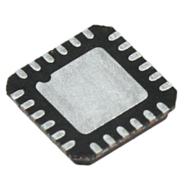
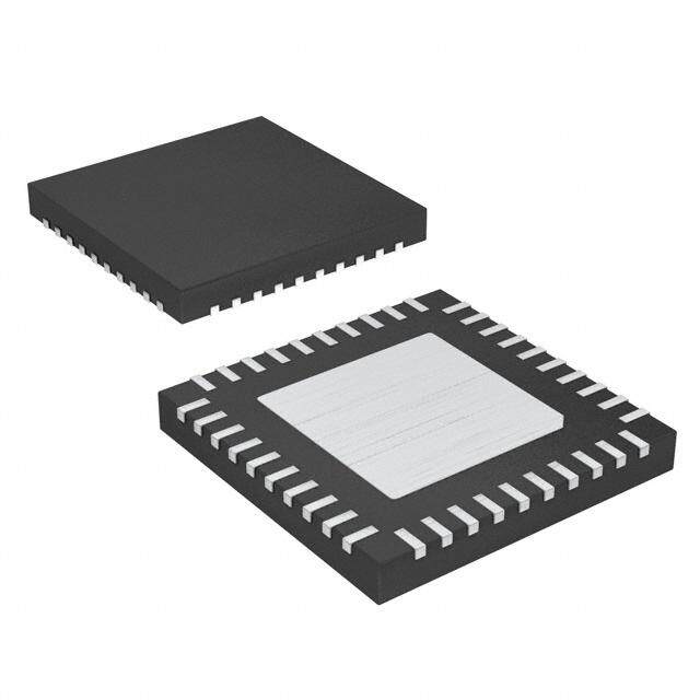
QProx™ QT60168, QT60248 lQ 16, 24 K QM ™ IC EY ATRIX s (cid:122) Second generation charge-transfer QMatrix technology (cid:122) Keys individually adjustable for sensitivity, response /R Y Y Y Y X X X S 2 1 0 2 time, and many other critical parameters 2 1 0 T A A A B (cid:122) Panel thicknesses to 50mm through any dielectric 32 31 30 2928 27 26 25 (cid:122) 16 and 24 touch key versions X3 1 24 Y1B X4 2 23 Y0B (cid:122) 100% autocal for life - no adjustments required VSS 3 QT60248 22 n/c (cid:122) SPI slave interface VDD 4 QT60168 21 VSS (cid:122) Adjacent key suppression feature VSS 5 20 VDD (cid:122) Synchronous noise suppression feature VDD 6 TQFP-32 19 SYNC (cid:122) Spread-spectrum modulation - high noise immunity X5 7 18 VDD (cid:122) Mix and match key sizes & shapes in one panel X6 8 17 SCK 9 10 11 12 13 14 15 16 (cid:122) Low overhead communications protocol (cid:122) FMEA compliant design features X V S S D /S M M (cid:122) Negligible external component count 7 REF _SYN MP RDY S OSI ISO (cid:122) Extremely low cost per key C (cid:122) +3 to +5V single supply operation (cid:122) 32-pin lead-free TQFP package APPLICATIONS (cid:121) Security keypanels (cid:121) Appliance controls (cid:121) ATM machines (cid:121) Automotive panels (cid:121) Industrial keyboards (cid:121) Outdoor keypads (cid:121) Touch-screens (cid:121) Machine tools These digital charge-transfer (“QT”) QMatrix™ ICs are designed to detect human touch on up to 16 or 24 keys when used with a scanned, passive X-Y matrix. They will project touch keys through almost any dielectric, e.g. glass, plastic, stone, ceramic, and even wood, up to thicknesses of 5 cm or more. The touch areas are defined as simple 2-part interdigitated electrodes of conductive material, like copper or screened silver or carbon deposited on the rear of a control panel. Key sizes, shapes and placement are almost entirely arbitrary; sizes and shapes of keys can be mixed within a single panel of keys and can vary by a factor of 20:1 in surface area. The sensitivity of each key can be set individually via simple functions over the serial port by a host microcontroller. Key setups are stored in an onboard eeprom and do not need to be reloaded with each powerup. These devices are designed specifically for appliances, electronic kiosks, security panels, portable instruments, machine tools, or similar products that are subject to environmental influences or even vandalism. They permit the construction of 100% sealed, watertight control panels that are immune to humidity, temperature, dirt accumulation, or the physical deterioration of the panel surface from abrasion, chemicals, or abuse. To this end they contain Quantum-pioneered adaptive auto self-calibration, drift compensation, and digital filtering algorithms that make the sensing function robust and survivable. These devices feature continuous FMEA self-test and reporting diagnostics, to allow their use in critical consumer appliance applications, for example ovens and cooktops. Common PCB materials or flex circuits can be used as the circuit substrate; the overlying panel can be made of any non-conducting material. External circuitry consists of only a few passive parts. Control and data transfer is via an SPI port. These devices makes use of an important new variant of charge-transfer sensing, transverse charge-transfer, in a matrix format that minimizes the number of required scan lines. Unlike older methods, it does not require one IC per key. AVAILABLE OPTIONS T # Keys Part Number Lead-Free A -400C to +1050C 16 QT60168-ASG Yes -400C to +1050C 24 QT60248-ASG Yes LQ Copyright © 2004 QRG Ltd QT60248-AS R4.02/0405
Contents 1 Overview . . . . . . . . . . . . . . . . . . . . . . . . . . . . . . 3 4.9 Report FMEA Status - 0x0c . . . . . . . . . . . . . . . . . . . 13 1.1 Part differences . . . . . . . . . . . . . . . . . . . . . . . . . 3 4.10 Dump Setups Block - 0x0d . . . . . . . . . . . . . . . . . . . 13 1.2 Enabling / Disabling Keys . . . . . . . . . . . . . . . . . . . . 3 4.11 Eeprom CRC - 0x0e . . . . . . . . . . . . . . . . . . . . . . 13 2 Hardware & Functional . . . . . . . . . . . . . . . . . . . . . 3 4.12 Return Last Command - 0x0f . . . . . . . . . . . . . . . . . . 13 2.1 Matrix Scan Sequence . . . . . . . . . . . . . . . . . . . . . . 3 4.13 Internal Code - 0x10 . . . . . . . . . . . . . . . . . . . . . . 13 2.2 Disabling Keys; Burst Paring . . . . . . . . . . . . . . . . . . . 3 4.14 Internal Code - 0x12 . . . . . . . . . . . . . . . . . . . . . . 13 2.3 Response Time . . . . . . . . . . . . . . . . . . . . . . . . . 3 4.15 Data Set for One Key - 0x4k . . . . . . . . . . . . . . . . . . 14 2.4 Oscillator . . . . . . . . . . . . . . . . . . . . . . . . . . . . 4 4.16 Status for Key ‘k’ - 0x8k . . . . . . . . . . . . . . . . . . . . 14 2.5 Sample Capacitors; Saturation . . . . . . . . . . . . . . . . . 4 4.17 Cal Key ‘k’ - 0xck . . . . . . . . . . . . . . . . . . . . . . . . 14 2.6 Sample Resistors . . . . . . . . . . . . . . . . . . . . . . . . 4 4.18 Command Sequencing . . . . . . . . . . . . . . . . . . . . . 14 2.7 Signal Levels . . . . . . . . . . . . . . . . . . . . . . . . . . 4 Table 4.2 Command Summary . . . . . . . . . . . . . . . . . . . . 16 2.8 Matrix Series Resistors . . . . . . . . . . . . . . . . . . . . . 5 5 Setups . . . . . . . . . . . . . . . . . . . . . . . . . . . . . . . 18 2.9 Key Design . . . . . . . . . . . . . . . . . . . . . . . . . . . 5 5.1 Negative Threshold - NTHR . . . . . . . . . . . . . . . . . . . 18 2.10 PCB Layout, Construction . . . . . . . . . . . . . . . . . . . 6 5.2 Positive Threshold - PTHR . . . . . . . . . . . . . . . . . . . 18 2.10.1 LED Traces and Other Switching Signals . . . . . . . . . . . . 6 5.3 Drift Compensation - NDRIFT, PDRIFT . . . . . . . . . . . . . 18 2.10.2 PCB Cleanliness . . . . . . . . . . . . . . . . . . . . . . . 6 5.4 Detect Integrators - NDIL, FDIL . . . . . . . . . . . . . . . . . 19 2.11 Power Supply Considerations . . . . . . . . . . . . . . . . . 6 5.5 Negative Recal Delay - NRD . . . . . . . . . . . . . . . . . . . 19 2.12 Startup / Calibration Times . . . . . . . . . . . . . . . . . . . 6 5.6 Positive Recalibration Delay - PRD . . . . . . . . . . . . . . . 19 Table 2-1 Basic Timings . . . . . . . . . . . . . . . . . . . . . . 6 5.7 Burst Length - BL . . . . . . . . . . . . . . . . . . . . . . . . 20 2.13 Reset Input . . . . . . . . . . . . . . . . . . . . . . . . . . 6 5.8 Adjacent Key Suppression - AKS . . . . . . . . . . . . . . . . 20 2.14 Spread Spectrum Acquisitions . . . . . . . . . . . . . . . . . 7 5.9 Oscilloscope Sync - SSYNC . . . . . . . . . . . . . . . . . . . 20 2.15 Detection Integrators . . . . . . . . . . . . . . . . . . . . . . 7 5.10 Mains Sync - MSYNC . . . . . . . . . . . . . . . . . . . . . 20 2.16 FMEA Tests . . . . . . . . . . . . . . . . . . . . . . . . . . 7 5.11 Burst Spacing - BS . . . . . . . . . . . . . . . . . . . . . . . 20 2.17 Wiring . . . . . . . . . . . . . . . . . . . . . . . . . . . . . 8 5.12 Lower Signal Limit - LSL . . . . . . . . . . . . . . . . . . . . 21 Table 2.2 - Pin Listing . . . . . . . . . . . . . . . . . . . . . . . 8 5.13 Host CRC - HCRC . . . . . . . . . . . . . . . . . . . . . . . 21 Figure 2.7 Wiring Diagram . . . . . . . . . . . . . . . . . . . . . . 9 Table 5.1 Setups Block . . . . . . . . . . . . . . . . . . . . . . . 22 3 Serial Communications . . . . . . . . . . . . . . . . . . . . . 10 Table 5.2 Key Mapping . . . . . . . . . . . . . . . . . . . . . . . 22 3.1 DRDY Pin . . . . . . . . . . . . . . . . . . . . . . . . . . . . 10 Table 5.3 Setups Block Summary . . . . . . . . . . . . . . . . . . 23 3.2 SPI Communications . . . . . . . . . . . . . . . . . . . . . . 10 6 Specifications . . . . . . . . . . . . . . . . . . . . . . . . . . 24 3.3 Command Error Handling . . . . . . . . . . . . . . . . . . . . 11 6.1 Absolute Maximum Electrical Specifications . . . . . . . . . . . 24 4 Control Commands . . . . . . . . . . . . . . . . . . . . . . . 11 6.2 Recommended operating conditions . . . . . . . . . . . . . . . 24 4.1 Null Command - 0x00 . . . . . . . . . . . . . . . . . . . . . . 11 6.3 DC Specifications . . . . . . . . . . . . . . . . . . . . . . . . 24 4.2 Enter Setups Mode - 0x01 . . . . . . . . . . . . . . . . . . . . 12 6.4 Timing Specifications . . . . . . . . . . . . . . . . . . . . . . 24 4.3 Cal All - 0x03 . . . . . . . . . . . . . . . . . . . . . . . . . . 12 6.5 Mechanical Dimensions . . . . . . . . . . . . . . . . . . . . . 24 4.4 Force Reset - 0x04 . . . . . . . . . . . . . . . . . . . . . . . 12 6.6 Marking . . . . . . . . . . . . . . . . . . . . . . . . . . . . . 25 4.5 General Status - 0x05 . . . . . . . . . . . . . . . . . . . . . . 12 7 Appendix . . . . . . . . . . . . . . . . . . . . . . . . . . . . . 26 4.6 Report 1st Key - 0x06 . . . . . . . . . . . . . . . . . . . . . . 13 7.1 8-Bit CRC Algorithm . . . . . . . . . . . . . . . . . . . . . . . 26 4.7 Report Detections for All Keys - 0x07 . . . . . . . . . . . . . . 13 7.2 1-Sided Key Layout . . . . . . . . . . . . . . . . . . . . . . . 27 Table 4.1 Bits for key reporting and numbering . . . . . . . . . . . . 13 7.3 PCB Layout . . . . . . . . . . . . . . . . . . . . . . . . . . . 27 4.8 Report Error Flags for All Keys - 0x0b . . . . . . . . . . . . . . 13 lQ 2 QT60248-AS R4.02/0405
1.2 Enabling / Disabling Keys 1 Overview The NDIL parameter is used to enable and disable keys in the QMatrix devices are digital burst mode charge-transfer (QT) matrix. Setting NDIL = 0 for a key disables it (Section 5.4). At sensors designed specifically for matrix geometry touch no time can the number of enabled keys exceed the maximum controls; they include all signal processing functions necessary specified for the device in the case of the QT60168. to provide stable sensing under a wide variety of changing conditions. Only a few external parts are required for operation. On the QT60168, only the first 2 Y lines (Y0, Y1) are The entire circuit can be built within a few square centimeters of operational by default. On the QT60168, to use keys located on single-sided PCB area. CEM-1 and FR1 punched, single-sided line Y2, one or more of the pre-enabled keys must be disabled materials can be used for possible lowest cost. The PCB’s rear simultaneously while enabling the desired new keys. This can can be mounted flush on the back of a glass or plastic panel be done in one Setups block load operation. using a conventional adhesive, such as 3M VHB 2-sided adhesive acrylic film. 2 Hardware & Functional Figure 1-1 Field flow between X and Y elements 2.1 Matrix Scan Sequence overlying panel The circuit operates by scanning each key sequentially, key by key. Key scanning begins with location X=0 / Y=0 (key #0). X axis keys are known as rows while Y axis keys are referred to as columns. Keys are scanned sequentially by row, for example X Y the sequence X0Y0 X1Y0 .... X7Y0, X0Y1, X1Y1... etc. Keys are element element also numbered from 0..24. Key 0 is located at X0Y0. A table of key numbering is located on page 22. Each key is sampled in a burst of acquisition pulses whose length is determined by the Setups parameter BL (page 20), which can be set on a per-key basis. A burst is completed entirely before the next key is sampled; at the end of each burst QMatrix parts employ transverse charge-transfer ('QT') sensing, the resulting signal is converted to digital form and processed. a technology that senses changes in electrical charge forced The burst length directly impacts key gain; each key can have a across an electrode by a pulse edge (Figure 1-1). QMatrix unique burst length in order to allow tailoring of key sensitivity devices allow for a wide range of key sizes and shapes to be on a key by key basis. mixed together in a single touch panel. The devices use an SPI interface to allow key data to be 2.2 Disabling Keys; Burst Paring extracted and to permit individual key parameter setup. The Keys that are disabled by setting NDIL =0 (Section 5.4, page interface protocol uses simple single byte commands and 19) have their bursts pared from the scan sequence to save responds with single byte responses in most cases. The time. This has the consequence of affecting the scan rate of the command structure is designed to minimize the amount of data entire matrix as well as the time required for initial matrix traffic while maximizing the amount of information conveyed. calibration. In addition to normal operating and setup functions the device Reducing the number of enabled keys also reduces the time can also report back actual signal strengths and error codes. required to calibrate an individual key once the matrix is initially QmBtn software for the PC can be used to program the calibrated after power-up or reset, since the total cycle time is operation of the IC as well as read back key status and signal proportional to the number of enabled keys. levels in real time. Keys that are disabled report as follows: The QT60168 and QT60248 are electrically identical with the Signal = 0 exception of the number of keys which may be sensed. Reference = 0 Low-signal error flag (provided LSL >0) 1.1 Part differences Calibrating flag for key set only just after device reset or Versions of the device are capable of a maximum of 16 or 24 after a CAL command, for one scan cycle only keys (QT60168, QT60248 respectively). Failed calibration error for key always set Detect flag for key never set These devices are identical in all respects, except that each is capable of only the number of keys specified. These keys can See also Section 4.16 notes. be located anywhere within the electrical grid of 8 X and 3 Y 2.3 Response Time scan lines. The response time of the device depends on the scan rate of Unused keys are always pared from the burst sequence in the keys (Section 5.11), the number of keys enabled (Section order to optimize speed. Similarly, in a given part a lesser 5.4), the detect integrator settings (Section 5.4), the serial number of enabled keys will cause any unused acquisition burst polling rate by the host microcontroller, and the time required to timeslots to be pared from the sampling sequence to optimize do FMEA tests at the end of each scan (~5ms). acquire speed. Thus, if only 14 keys are actually enabled, only 14 timeslots are used for scanning. lQ 3 QT60248-AS R4.02/0405
For example: 2.6 Sample Resistors NKE = Number of keys enabled = 20 There are 3 sample resistors (Rs) used to perform single-slope FDIL = Fast detect integrator limit = 5 ADC conversion of the acquired charge on each Cs capacitor. BS = Burst spacing = 0.5ms These resistors directly control acquisition gain: larger values of FMEA = FMEA test time = 5ms Rs will proportionately increase signal gain. Values of Rs can NDIL = Norm detect integrator Limit = 2 range from 380K ohms to 1M ohms. 470K ohms is a HPR = Host polling rate = 10ms reasonable value for most purposes. The worst case response time is computed as: Unused Y lines do not require an Rs resistor. Tr = ((((NKE + FDIL) * BS) + FMEA) * NDIL) + HPR 2.7 Signal Levels For the above example values: Quantum’s QmBtn™ software makes it is easy to observe the Tr = ((((20 + 5) * 0.5ms) + 5ms) * 2) + 10ms = 45ms absolute level of signal received by the sensor on each key. The signal values should normally be in the range from 250 to 2.4 Oscillator 750 counts with properly designed key shapes and values of Rs. However, long adjacent runs of X and Y lines can also The oscillator is internal to the device. There is no facility for artificially boost the signal values, and induce signal saturation: external clocking. this is to be avoided. The X-to-Y coupling should come mostly from intra-key electrode coupling, not from stray X-to-Y trace 2.5 Sample Capacitors; Saturation coupling. The charge sampler capacitors on the Y pins should be the QmBtn software is available free of charge on Quantum’s values shown. They should be X7R or NP0 ceramics or PPS website. film. The value of these capacitors is not critical but 4.7nF is recommended for most cases. The signal swing from the smallest finger touch should preferably exceed 10 counts, with 15 being a reasonable target. Cs voltage saturation is shown in Figure 2-1. This nonlinearity The signal threshold setting (NTHR) should be set to a value is caused by excessively negative voltage on Cs inducing guaranteed to be less than the signal swing caused by the conduction in the pin protection diodes. This badly saturated smallest touch. signal destroys key gain and introduces a strong thermal coefficient which can cause 'phantom' detection. The cause of this is usually from the burst length being too long, the Cs value being too small, or the X-Y coupling being too large. Solutions include loosening up the interdigitation of key structures, Figure 2-1 VCs - Non-Linear During Burst separating X and Y lines on the PCB more, increasing Cs, and (Burst too long, or Cs too small, or X-Y capacitance too large) decreasing the burst length. Increasing Cs will make the part slower; decreasing burst length will make it less sensitive. A better PCB layout and a looser key structure (up to a point) have no negative effects. Cs voltages should be observed on an oscilloscope with the matrix layer bonded to the panel material; if the Rs side of any Cs ramps more negative than -0.25 volts during any burst (not counting overshoot spikes which are probe artifacts), there is a potential saturation problem. Figure 2-2 shows a defective waveform similar to that of 2-1, Figure 2-2 VCs - Poor Gain, Non-Linear During Burst but in this case the distortion is caused by excessive stray (Excess capacitance from Y line to Gnd) capacitance coupling from the Y line to AC ground, for example from running too near and too far alongside a ground trace, ground plane, or other traces. The excess coupling causes the charge-transfer effect to dissipate a significant portion of the received charge from a key into the stray capacitance. This phenomenon is more subtle; it can be best detected by increasing BL to a high count and watching what the waveform does as it descends towards and below -0.25V. The waveform will appear deceptively straight, but it will slowly start to flatten even before the -0.25V level is reached. A correct waveform is shown in Figure 2-3. Note that the Figure 2-3 Vcs - Correct bottom edge of the bottom trace is substantially straight (ignoring the downward spikes). Unlike other QT circuits, the Cs capacitor values on QT60xx8 devices have no effect on conversion gain. However they do affect conversion time. Unused Y lines should be left open. lQ 4 QT60248-AS R4.02/0405
Figure 2-4 X-Drive Pulse Roll-off and Dwell Time Figure 2-6 Recommended Key Structure ‘T’ should ideally be similar to the complete thickness the fields need to penetrate to the touch surface. Smaller dimensions will also work but will give less signal strength. If in doubt, make the pattern coarser. X drive Lost charge due to inadequate settling before end of dwell time Dwell time Y gate Figure 2-5 Probing X-Drive Waveforms With a Coin The upper limits of Rx and Ry are reached when the signal level and hence key sensitivity are clearly reduced. The limits of Rx and Ry will depending on key geometry and stray capacitance, and thus an oscilloscope is required to determine optimum values of both. The upper limit of Rx can vary depending on key geometry and stray capacitance, and some experimentation and an oscilloscope are required to determine optimum values. Dwell time is the duration in which charge coupled from X to Y is captured. Increasing Rx values will cause the leading edge of the X pulses to increasingly roll off, causing the loss of captured charge (and hence loss of signal strength) from the keys (Figure 2-4). The dwell time of these parts is fixed at 375ns. If the X pulses have not settled within 375ns, key gain will be reduced; if this happens, either the stray capacitance on the X line(s) should be reduced (by a layout change, for example by reducing X line exposure to nearby ground planes or traces), or, the Rx resistor needs to be reduced in value (or a combination of both approaches). Increasing the burst length (BL) parameter will increase the One way to determine X line settling time is to monitor the fields signal strengths as will increasing the sampling resistor (Rs) using a patch of metal foil or a small coin over the key (Figure values. 2-5). Only one key along a particular X line needs to be observed, as each of the keys along that X line will be identical. 2.8 Matrix Series Resistors The 250ns dwell time should be exceed the observed 95% settling of the X-pulse by 25% or more. The X and Y matrix scan lines should use series resistors (referred to as Rx and Ry respectively) for improved EMI In almost all case, Ry should be set equal to Rx, which will performance. ensure that the charge on the Y line is fully captured into the Cs capacitor. X drive lines require them in most cases to reduce edge rates and thus reduce RF emissions. Typical values range from 1K to 20K ohms. 2.9 Key Design Y lines need them to reduce EMC susceptibility problems and in Circuits can be constructed out of a variety of materials some extreme cases, ESD. Typical Y values range around 1K including flex circuits, FR4, and even inexpensive single-sided ohms. Y resistors act to reduce noise susceptibility problems by CEM-1. forming a natural low-pass filter with the Cs capacitors. The actual internal pattern style is not as important as is the It is essential that the Rx and Ry resistors and Cs capacitors be need to achieve regular X and Y widths and spacings of placed very close to the chip. Placing these parts more than a sufficient size to cover the desired graphical key area or a little few millimeters away opens the circuit up for high frequency bit more; ~3mm oversize is acceptable in most cases, since the interference problems (above 20MHz) as the trace lengths key’s electric fields drop off near the edges anyway. The overall between the components and the chip start to act as RF key size can range from 10mm x 10mm up to 100mm x 100mm antennae. but these are not hard limits. The keys can be any shape including round, rectangular, square, etc. The internal pattern lQ 5 QT60248-AS R4.02/0405
can be as simple as a single bar of Y within a solid perimeter of solder joints, causing signal drift and resultant false detections X, or (preferably) interdigitated as shown in Figure 2-6. or transient losses of sensitivity or instability. Conformal coatings will trap in existing amounts of moisture which will then For better surface moisture suppression, the outer perimeter of become highly temperature sensitive. X should be as wide as possible, and there should be no ground planes near the keys. The variable ‘T’ in this drawing The designer should specify ultrasonic cleaning as part of the represents the total thickness of all materials that the keys must manufacturing process, and in cases where a high level of penetrate. humidity is anticipated, the use of conformal coatings after cleaning to keep out moisture. See Figure 2-6 and page 27 for examples of key layouts. See Section 2.16 for guidance about potential FMEA problems 2.11 Power Supply Considerations with small key shapes. As these devices use the power supply itself as an analog reference, the power should be very clean and come from a 2.10 PCB Layout, Construction separate regulator. A standard inexpensive LDO type regulator It is best to place the chip near the touch keys on the same should be used that is not also used to power other loads such PCB so as to reduce X and Y trace lengths, thereby reducing as LEDs, relays, or other high current devices. Load shifts on the chances for EMC problems. Long connection traces act as the output of the LDO can cause Vdd to fluctuate enough to RF antennae. The Y (receive) lines are much more susceptible cause false detection or sensitivity shifts. to noise pickup than the X (drive) lines. A single ceramic 0.1uF bypass capacitor should be placed very Even more importantly, all signal related discrete parts (R’s and close to supply pins 3, 4, 5 and 6 of the IC. Pins 18, 20, and 21 C’s) should be very close to the body of the chip. Wiring do not require bypassing. between the chip and the various R’s and C’s should be as Vdd can range from +3 to +5 nominal. The device enters reset short and direct as possible to suppress noise pickup. below 2.8V via an internal LVD circuit. See Section 2.13. 2.12 Startup / Calibration Times The devices require initialization times as follows: Ground planes and traces should NOT be used around the keys and the Y lines Normal cold start to ability to communicate: from the keys. Ground areas, traces, and 4ms - Normal initialization from any type of reset other adjacent signal conductors that act as AC ground (such as Vdd and LED 22ms - Initialization from reset where the Setups were drive lines etc) will absorb the received key signals previously modified. and reduce signal-to-noise ratio (SNR) and thus will Calibration time per key vs. burst spacings for 16 and 24 be counterproductive. Ground planes around keys will enabled keys: also make water film effects worse. Table 2-1 Basic Timings Burst Spacing, Cal Time, ms, Cal Time, ms, Ground planes, if used, should be placed under or around the ms 16 keys 24 keys QT chip itself and the associated R’s and C’s in the circuit, 0.50 176 228 under or around the power supply, and back to a connector, but 0.75 231 309 nowhere else. 1.00 286 390 1.25 342 472 See page 27 for an example of a 1-sided PCB layout. 1.50 397 553 1.75 452 634 2.10.1 LED Traces and Other Switching Signals 2.00 507 715 Digital switching signals near the Y lines will induce transients 2.25 563 797 into the acquired signals, deteriorating the SNR perfomance of 2.50 618 878 the device. Such signals should be routed away from the Y 2.75 673 959 lines, or the design should be such that these lines are not 3.00 728 1,040 switched during the course of signal acquisition (bursts). To the above, add the initialization time from above (4ms or LED terminals which are multiplexed or switched into a floating 22ms) to get the total elapsed time from reset, to the ability to state and which are within or physically very near a key report key detections over the serial interface. Disabled keys structure (even if on another nearby PCB) should be bypassed are subtracted from the burst sequence and thus the cal time is to either Vss or Vdd with at least a 10nF capacitor of any type, shortened. The scan time should be measured on an to suppress capacitive coupling effects which can induce false oscilloscope. signal shifts. Led terminals which are constantly connected to Keys that cannot calibrate for some reason require 5 full cal Vss or Vdd do not need further bypassing. cycles before they report as errors. The device can report back during the calibration interval that the key(s) affected are still in 2.10.2 PCB Cleanliness calibration via status function bits. Errors can be observed after All capacitive sensors should be treated as highly sensitive a cal cycle using the 0x8k command (see Section 4.16). circuits which can be influenced by stray conductive leakage paths. QT devices have a basic resolution in the femtofarad 2.13 Reset Input range; in this region, there is no such thing as ‘no clean flux’. Flux absorbs moisture and becomes conductive between The /RST pin can be used to reset the device to simulate a power down cycle, in order to bring the part up into a known lQ 6 QT60248-AS R4.02/0405
state should communications with the part be lost. The pin is analysis is being applied increasingly to a wide variety of active low, and a low pulse lasting at least 10µs must be applications including domestic appliances. To survive FMEA applied to this pin to cause a reset. testing the control board must survive any single problem in a way that the overall product can either continue to operate in a To provide for proper operation during power transitions the safe way, or shut down. devices have an internal LVD set to 2.7 volts. The most common FMEA requirements regard opens and The reset pin has an internal 30K ~ 80K resistor. A 2.2µF shorts analysis of adjacent pins on components and capacitor plus a diode to Vdd can be connected to this pin as a connectors. However other criteria must usually be taken into traditional reset circuit, but this is not required. account, for example complete device failure, and the use of A Force Reset command, 0x04 is also provided which redundant signaling paths. generates an equivalent hardware reset. QT60xx8 devices incorporate special self-test features which If an external hardware reset is not used, the reset pin may be allow products to pass such FMEA tests easily. These tests are connected to Vdd or left floating. performed during a dummy timeslot after the last enabled key. The FMEA testing is done on all enabled keys in the matrix, and 2.14 Spread Spectrum Acquisitions results are reported via the serial interface through a dedicated QT60xx8 devices use spread-spectrum burst modulation. This status command (page 13). Disabled keys are not tested. The has the effect of drastically reducing the possibility of EMI existence of an error is also reported in normal key reporting effects on the sensor keys, while simultaneously spreading RF commands such as Report 1st Key, page 13. emissions. This feature is hard-wired into the device and All FMEA tests are repeated every second or faster during cannot be disabled or modified. normal run operation. Sometimes, FMEA errors can occur Spread spectrum is configured as a frequency chirp over a intermittently, for example due to momentary power wide range of frequencies for robust operation. fluctuations. It is advisable to confirm a true FMEA fault condition by making sure the error flags persist for a several seconds. 2.15 Detection Integrators See also Section 5.4, page 19. Since the devices only communicate in slave mode, the host can determine immediately if the QT has suffered a The devices feature a detection integration mechanism, which catastrophic failure. acts to confirm a detection in a robust fashion. The basic idea is to increment a per-key counter each time the key has crossed The FMEA tests performed are: its threshold. When this counter reaches a preset limit the key (cid:131) X drive line shorts to Vdd and Vss is finally declared to be touched. Example: If the limit value is 10, then the device has to detect a threshold crossing 10 times (cid:131) X drive line shorts to other pins in succession without interruption, before the key is declared to (cid:131) X drive signal deviation be touched. If on any sample the signal is not seen to cross the threshold level, the counter is cleared and the process has to (cid:131) Y line shorts to Vdd and Vss start over from the beginning. (cid:131) Y line shorts to other pins The QT60xx8 uses a two-tier confirmation mechanism having (cid:131) X to Y line shorts two such counters for each key. These can be thought of as ‘inner loop’ and ‘outer loop’ confirmation counters. (cid:131) Cs capacitor checks including shorts and opens The ‘inner’ counter is referred to as the ‘fast-DI’; this acts to (cid:131) Vref test attempt to confirm a detection via rapid successive acquisition (cid:131) Key gain test bursts, at the expense of delaying the sampling of the next key. Each key has its own fast-DI counter and limit value; these Other tests incorporated into the devices include: limits can be changed via the Setups block on a per-key basis. (cid:131) A test for signal levels against a preset min value (LSL The ‘outer’ counter is referred to as the ‘normal-DI’; this DI setup, see page 21). If any signal level falls below this counter increments whenever the fast-DI counter has reached level, an error flag is generated. its limit value. If a fast-DI counter failed to reach its terminal (cid:131) CRC communications checks on all critical command and count, the corresponding normal-DI counter is also reset. The data transmissions. normal-DI counter also has a limit value which is settable on a per-key basis. If a normal-DI counter reaches its terminal count, (cid:131) ‘Last-command’ command to verify that an instruction was the corresponding key is declared to be touched and becomes properly received. ‘active’. Note that the normal-DI can only be incremented once Some very small key designs have very low X-Y coupling. In per complete keyscan cycle, ie more slowly, whereas the these cases, the amount of signal will be very small, and the fast-DI is incremented ‘on the spot’ without interruption. key gain will be low. As a result, small keys can fail the LSL The net effect of this mechanism is a multiplication of the inner test (page 21) or the FMEA key gain test (above). In such and outer counters and hence a highly noise-resistance cases, the burst length of the key should be increased so that sensing method. If the inner limit is set to 5, and the outer to 3, the key gain increases. Failing that, a small ceramic capacitor, the net effect is 5x3=15 successive threshold crossings to for example 3pF, can be added between the X and Y lines declare a key as active. serving the key to artificially boost signal strength. For those applications requiring it, Quantum can supply sample 2.16 FMEA Tests FMEA test data on special request. FMEA (Failure Modes and Effects Analysis) is a tool used to determine critical failure problems in control systems. FMEA lQ 7 QT60248-AS R4.02/0405
2.17 Wiring Table 2.2 - Pin Listing Pin Function I/O Comments If Unused, Connect To.. 1 X3 O X3 matrix drive line Leave open 2 X4 O X4 matrix drive line Leave open 3 Vss P Supply ground - 4 Vdd P Power, +3 ~ +5V - 5 Vss P Supply ground - 6 Vdd P Power, +3 ~ +5V - 7 X5 O X5 matrix drive line Leave open 8 X6 O X6 matrix drive line Leave open 9 X7 O X7 matrix drive line Leave open 10 Vref I 0.05V nominal +/-10% via external divider - 11 S_Sync O Scope Sync: Synchronization test signal output Leave open 12 SMP O Sample drive output - 1= Comms ready; 13 DRDY O - has internal 20K ~ 50K pull-up SPI slave select; 14 /SS I - has internal 20K ~ 50K pull-up 15 MOSI I SPI data input - 16 MISO O SPI data output - 17 SCK I SPI clock input - 18 Vdd P Power, +3 ~ +5V - 19 SYNC I Mains sync input Vdd 20 Vdd P Power, +3 ~ +5V - 21 Vss P Supply ground - 22 NC N/A Not used Leave open 23 Y0B I Y0B line connection Leave open 24 Y1B I Y1B line connection 25 Y2B I Y2B line connection Leave open 26 Y0A I Y0A line connection 27 Y1A I Y1A line connection Leave open 28 Y2A I Y2A line connection Reset low; 29 /RST I Leave open or Vdd has internal 30K ~ 80K pull-up 30 X0 O X0 matrix drive line Leave open 31 X1 O X1 matrix drive line Leave open 32 X2 O X2 matrix drive line Leave open lQ 8 QT60248-AS R4.02/0405
Figure 2.7 Wiring Diagram See Table 2.2 for further connection information. VDD +3 to +5V Note 1 Vunreg VREG + + 100nF 4.7uF 4.7uF RX7 1K E V RX6 1K RI DRDY D PI MOSSSI RX5 1KRX4 1K RIX X S MISO RX3 1K AT M RX2 1K SCLK RX1 1K RX0 1K SCOPE SYNC QT60248 QT60168 LINE SYNC N RY0 1K N I A CS0 4.7nF C S Y RY1 1K X RI T CS1 4.7nF A Note 2 M RY2 1K Note 2 CS2 4.7nF Note 1: Wire 100nF bypass cap RS2 RS1 RS0 very close to pins 3, 4, 5, 6 10K VDD 470K 470K 470K Note 2: Leave Y2A, Y2B unconnected 100 for QT60168 lQ 9 QT60248-AS R4.02/0405
The time it takes for DRDY to go high again after a command 3 Serial Communications depends on the command. Following is a list of commands and These devices use SPI communications, in slave mode. the time required to process them and then raise DRDY: The host device always initiates communications sequences; 0x0E Eeprom CRC [ 25ms the QT is incapable of chattering data back to the host. This is 0x01 Load Setups [ 25ms intentional for FMEA purposes so that the host always has total All other commands: [ 2ms between bytes; control over the communications with the QT60xx8. In SPI [ 40µs after CRC byte is sent mode the device is a slave, so that even return data following a Other DRDY specs: command is controlled by the host. Min time DRDY is low: 1µs A command from the host always ends in a response of some Min time DRDY is low kind from the QT. Some transmission types from the host or the after reset: 1ms QT employ a CRC check byte to provide for robust communications. 3.2 SPI Communications A DRDY line is provided that handshakes transmissions. SPI communications operates in slave mode only, and obeys Generally this is needed by the host from the QT to ensure that DRDY control signaling. The clocking is as follows: transmissions are not sent when the QT is busy or has not yet processed a prior command. Clock idle: High Clock shift out edge: Falling Initiating or Resetting Communications: After a reset, or, Clock data in edge: Rising should communications be lost due to noise or out-of-sequence Max clock rate: 1.5MHz reception, the host should send a 0x0f (return last command) command repeatedly until the compliment of 0x0f, i.e. 0xf0, is SPI mode requires 5 signals to operate: received back. Then, the host can resume normal run mode MOSI - Master out / Slave in data pin; used as an input for communications from a clean start. data from the host (master). This pin should be connected Poll rate: The typical poll rate in normal ‘run’ operation should to the MOSI (DO) pin of the host device. be no faster than once per 10ms; 25ms is more than fast MISO - Master in / Slave out data pin; used as an output for enough to extract status data using the 0x06 command (report data to the host. This pin should be connected to the MISO first key: see page 13) in most situations. Streaming multi-byte response commands like the 0x0d command (dump setups: see page 13) or multi-byte response commands like 0x07 can and should pace at the maximum possible rate. Figure 3-1 Basic SPI Connections Run Poll Sequence: In normal run mode the host should limit HostMCU QT60xx8 traffic with a minimalist control structure (see also Section 4.18). The host should just send a 0x06 command until something P_IN DRDY requires a deeper state inspection. If there is more than one key in detect, the host should use 0x07 to find which additional keys P_OUT SS are in detect. If there is an error, the host should ascertain the SCK SCK error type based on commands 0x0b and 0x0c and take appropriate action. Issuing a 0x07 command all the time is MISO MISO wasteful of bandwidth, requires more host processor time, and MOSI MOSI actually conveys less information (no error flags are sent via a 0x07 command). 3.1 DRDY Pin Figure 3-2 Filtered SPI Connections DRDY is an open-drain output with an internal 20K ~ 50K pullup HostMCU QT60xx8 Circuit resistor. P_IN DRDY X drives Serial communications pacing is controlled by this pin. The host Ra (1 of 8 is permitted to send data only when DRDY is high. After a byte P_OUT1 Ca SS shown) 1K Xn is received DRDY will always go low even if only for a few Ra microseconds; during this period the host should not send data. SCK Ca SCK Therefore, after each byte transmission the host should first Ra check that DRDY is high again. MISO Ca MISO Ra If the host desires to send a byte to the QT it should behave as Ca Y Lines Yn follows: MOSI Ra MOSI s(h1o owfn 3) 1K 1. If DRDY is low, wait Ca P_OUT2 RESET 2. If DRDY is high: send a command to QT 1K 3. Wait at least 40µs (time S5 in Figure 3-3: DRDY is 1nF guaranteed to go low before this 40µs expires) 4. Wait until DRDY is high (it may already be high again) Recommended Values of Ra & Ca 5. Send next command or a null byte 0x00 to QT SPI Clock Rate Ra Ca 1.5MHz 680 100pF 400kHz 1,000 270pF 100kHz 2,200 470pF 50kHz 2,200 1nF lQ 10 QT60248-AS R4.02/0405
(DI) pin of the host. MISO floats when /SS is high to allow 3.3 Command Error Handling multi-drop communications along with other slave parts. If an unrecognized command is received, the device will release SCK - SPI clock - input only clock from host. The host must DRDY high and the communications error flag will be set in the shift out data on the falling SCK edge; the QT60xx8 clocks General Status byte (see Section 4.5). data in on the rising edge. The QT60xx8 likewise shifts data out on the falling edge of SCK back to the host so that the host can shift the data in on the rising edge. Important: 4 Control Commands SCK must idle high; it should never float. Refer to Table 4.2, page 16 for further details. /SS - Slave select - input only; acts as a framing signal to the sensor from the host. /SS must be low before and during The devices feature a set of commands which are used for reception of data from the host. It must not go high again control and status reporting. The host device has to send the until the SCK line has returned high; /SS must idle high. command to the QT60xx8 and await a response. This pin includes an internal pull-up resistor of 20K ~ 50K. SPI mode: While waiting the host should delay for 40µs from When /SS is high, MISO floats. the end of the command, then start to check if DRDY is or goes DRDY - Data Ready - active-high - indicates to the host that high. If it is high, then the host master can clock out the the QT is ready to send or receive data. This pin idles high. resulting byte(s). This pin includes an internal pull-up resistor of 20K ~ 50K. Command timeouts: Where a command involves multi-byte In SPI mode this pin is an output only (i.e. open drain with transfers in either direction, each byte must be transmitted internal pull-up). within 100ms of the prior byte or the command will timeout. No The MISO pin on the QT floats in 3-state mode between bytes error is reported for this condition; the command simply ceases. when /SS is high. This facilitates multiple devices on one SPI Word return byte order: Where a word or long word is bus. returned (16 or 24 bit number or bit pattern) the low order byte Null Bytes: When the QT responds to a command with one or is sent or received first. more response bytes, the host should issue a null commands (0x00) to get the response bytes back. The host should not 4.1 Null Command - 0x00 send new commands until all the responses are accepted back from the QT from the prior command via nulls. Used to shift back data from the QT. Since the host device is always the master in SPI mode, and data is clocked in both New commands attempted during intermediate byte transfers directions, the Null command is required frequently to act as a are ignored. placeholder where the desire is to only get data back from the SPI Line Noise: In some designs it is necessary to run SPI QT, not to send a command. lines over ribbon cable across a lengthy distance on a PCB. In SPI communications, when the QT60xx8 responds to a This can introduce ringing, ground bounce, and other noise command with one or more response bytes, the host can issue problems which can introduce false SPI clocking or false data. a new command instead of a null on the last byte shift Simple RC networks and slower data rates as shown in Figure operation. 3-2 are helpful to resolve these issues. New commands during intermediate byte shift-out operations CRC checks have been added to critical commands in order to are ignored, and null bytes should always be used. detect transmission errors to a high level of certainty. Figure 3-3 SPI Slave-Only Mode Timing S1: m333ns S2: [20ns S3: m25ns S4: [20ns S5: [40µs S6: m1µs S7: m333ns S8: m333ns S9: m667ns S6 high via pullup-R DRDY (from QT) S1 S5 /SS (from Host) S3 S9 CLK (from Host) S7 S8 Data shifts in to QT on rising edge (Data from MHoOsSt)I ? 7 6 5 4 3 2 1 0 7 6 5 4 3 2 1 0 7 6 5 4 3 2 1 0 S2 {Command byte} S4 {optional 2nd command byte} {null byte or next command to get QT response} Data shifts out of QT on falling edge (Data fromM IQSTO) 3-state ? 7 6 5 4 3 2 1 0 3-state ? 7 6 5 4 3 2 1 0 ? 7 6 5 4 3 2 1 0 data response lQ 11 QT60248-AS R4.02/0405
4.2 Enter Setups Mode - 0x01 The host can monitor the progress of the reset by checking the status byte for recalibration, using command 0x05. The This command is used to initiate the Setups block transfer from complete reset sequence is as follows: Host to QT. 1. Reset command received by QT The command must be repeated 2x within 100ms or the 2. Response byte (0xFB) recovered by host command will fail; the repeating command must be sequential 3. DRDY floats high without any intervening command. After the 2nd 0x01 from the 4. 20ms elapses until device completes reset host, the QT will stop scanning keys and reply with the 5. DRDY clamped low character 0xFE. In SPI mode this character must be shifted out 6. 4ms or 22ms elapses - (see Section 2.12) by sending a null (0x00) from the host. This command 7. DRDY floats high again - device reset has completed suspends normal sensing starting from the receipt of the second 0x01. A failure of the command will cause a timeout. If the host does not recover the response byte in step 2, the QT device will self-reset within 2 seconds. Each byte in the block must arrive at the QT no later than 100ms after the previous one or a timeout will occur. 4.5 General Status - 0x05 Any timeout will cause the device to cancel the block load and go back to normal operation. This command returns the general status bits. They are as follows: If no response comes back, the command was not received and the device should preferably be reset from the host by hardware BIT Description reset just in case there are any other problems. 7 Reserved 6 1= communications error If 0xFE is received by the host, then the host should begin to 5 1= FMEA failure detected transmit the block of Setups to the QT. DRDY handshakes the 4 Reserved data. The delay between bytes can be as short as 10µs but the 3 1= mains sync error host can make it longer than this if required, but no more than 2 1= calibration has failed on an 100ms. The last byte the host should send is the CRC for the enabled key or, an LSL failure block of data only, ie the command itself should not be folded 1 1= any key in calibration into the CRC. 0 1= any key in detect After the block transfer the QT will check the CRC and respond with 0x00 if there was an error. Regardless, it will program the Notes: internal eeprom. If the CRC was correct it will reply with a Bit 7: Reserved second 0xFE after the eeprom was programmed. Bit 6: Set if a communications failure, such as an unrecognized At the end of the full block load sequence, the device restarts command. This bit can be reset by sending command 0x0f sensing without recalibration. It is highly recommended that (“last command command”) repeatedly until a response of 0xf0 the part be reset after a block load to allow the part to is received. properly initialize itself, clear any setup flags, using the reset command or the reset pin. Bit 5: Set if an FMEA error was detected during operation. See Section 2.16. A further amplification of what the FMEA error consisted of is described in Section 4.9. 4.3 Cal All - 0x03 This command must be repeated 2x within 100ms or the Bit 4: Reserved command will fail; the repeating command must be sequential Bit 3: Set if there was a mains sync error, for example there without any intervening command. was no Sync signal detected within the allotted 100ms amount After the 2nd 0x03 from the host, the QT will reply with the of time. See Section 5.10. This condition is not necessarily fatal character 0xFC. Shortly thereafter the device will recalibrate all to operation, however the device will operate very slowly and keys and restart operation. may suffer from noise problems if the sync feature was required for noise reasons. If no 0xFC comes back, the command was not properly received and the device should preferably be reset. Bit 2: Reports either a cal failure (failed in 5 sequential attempts) on any enabled key or, that an enabled key has a The host can monitor the progress of the recalibration by very low signal reference value, lower than the user-settable checking the status byte, using command 0x05. LSL value (Section 5.12). Disabled keys do not cause this bit 2 A key will show an error flag (via command 0x8k) indicating the error flag to be set even if they generate an error flag in the key has failed calibration if its signal is too noisy or if its signal is 0x8k response. below the low signal threshold. A key is deemed too noisy if, at Bit 1: Set if any key is in the process of calibrating. the end of calibration, the signal is no longer between its computed negative hysteresis level and positive thresholds. Bit 0: Set if any key is in detection (touched). A CRC byte is appended to the response to the 0x05 command; 4.4 Force Reset - 0x04 this CRC folds in the command value 0x05 itself initially. The command must be repeated 2x within 100ms or the command will fail; the repeating command must be sequential without any intervening command. After the 2nd 0x04, the QT will reply with the character 0xFB just prior to executing the reset operation. lQ 12 QT60248-AS R4.02/0405
4.6 Report 1st Key - 0x06 4.9 Report FMEA Status - 0x0c Reports the first or only key to be touched, plus indicates if Returns one byte which shows the FMEA error status of the X there are yet other keys that are also touched. and/or Y matrix scan lines. If an X line is in error, the corresponding bit (below) is set. If a Y line has an FMEA error, The return bits are as follows: the entire field is set to ones (0xFF). BIT Description Due to the physics of matrix wiring, a fault on any Y line will 7 1= more than 1 key is active cause faults to be reported on all X lines as well. It is not 6 1= any error condition is present possible to separate out these faults for reporting purposes. 5 Unused 4 Key bit 4 b7 b6 b5 b4 b3 b2 b1 b0 X7 X6 X5 X4 X3 X2 X1 X0 3 Key bit 3 2 Key bit 2 A CRC byte is appended to the response; this CRC folds in the 1 Key bit 1 command 0x0C itself initially. 0 Key bit 0 Sometimes, FMEA errors can occur intermittently, for example Bits 4..0 encode for the first detected key in range 0..23. If no due to momentary power fluctuations. It is advisable to confirm keys are active, these 5 bits are all 1’s (0x1F, 31 decimal when a true FMEA fault condition by making sure the error flags bits 5, 6, 7 are masked off). Disabled keys do not report as persist for a several seconds. active and do not generate an error flag in bit 6, even if they are For more information see Section 2.16. reporting an error via command 0x8k. If 2 or more keys in detection, bit 7 is set and the host should 4.10 Dump Setups Block - 0x0d interrogate the part via the 0x07 command to read out all the This command causes the device to dump the entire internal key detections. This one command should be the dominant Setups block back to the host. interrogation command in the host interface; further commands can be issued if the response to 0x06 warrants it. If the transfer is not paced faster than 100ms per byte the transfer will be aborted and the device will time out. This can A CRC byte is appended to the response; this CRC folds in the happen if the host is also controlling DRDY. command 0x06 itself initially. During the transfer, sensing is halted. Sensing is resumed after the command has finished. 4.7 Report Detections for All Keys - 0x07 Returns three bytes which indicate all keys in detection if any, An 8-bit CRC is appended to the response; this CRC is the as a bitfield; active keys report as 1’s.. Key 0 reports in bit 0 of same as the Setups table CRC. the first byte returned; key 23 is reported in bit 7 of the last byte returned. See Table 4.1 and Table 5.2. Disabled keys report as 4.11 Eeprom CRC - 0x0e inactive (0). This command returns the 8-bit CRC byte calculated from the A CRC byte is appended to the response; this CRC folds in the eeprom contents. The CRC sent back is the same CRC that is command 0x07 itself initially. appended to the end of the Setups block. Table 4.1 Bits for key reporting and numbering This command requires substantial amounts of time to process and return a result; it is not recommended to use this command Key # Bit Number (X line #) except perhaps on startup or very infrequently. 7 6 5 4 3 2 1 0 0 7 6 5 4 3 2 1 0 No CRC is appended to the response. Byte Number Returned 1 15 14 13 12 11 10 9 8 (Y line #) 2 23 22 21 20 19 18 17 16 4.12 Return Last Command - 0x0f This command returns the last received command character, in 1’s complement (inverted). If the command is repeated twice or more, it will return the inversion of 0x0f, 0xf0. 4.8 Report Error Flags for All Keys - 0x0b If a prior command was not valid or was corrupted, it will return Returns three bytes which show error flags as a bitfield for all the bad command as well. This command also will reset the keys. Key 0 reports in bit 0 of the first byte returned; key 23 is communications error flag (Section 4.5). reported in bit 7 of the last byte returned. See Table 4.1 and Table 5.2. No CRC is appended to the response. A key that is in calibration also is reported as an error in the response. The error flag is self-cleared once the key 4.13 Internal Code - 0x10 successfully exits from calibration. This command returns a 1-byte internal code. Important note: These error bits exclude FMEA error flags. A CRC byte is appended to the response; this CRC folds in the command 0x10 itself initially. A CRC byte is appended to the response; this CRC folds in the command 0x0b itself initially. 4.14 Internal Code - 0x12 This command returns an internal code byte of the part for factory diagnostic purposes. A response might take as long as 500ms. No CRC is appended to the response. lQ 13 QT60248-AS R4.02/0405
4.15 Data Set for One Key - 0x4k This command functions the same as 0x03 CAL command except this command only affects one key ‘k’ where ‘k’ is from 0 Returns the data set for key k, where k = {0..23} encoded into to 23. the low nibble of this command. This command returns 5 bytes, in the sequence: The chosen key ‘k’ is recalibrated in its native timeslot; normal running of the part is not interrupted and all other keys operate Signal (2 bytes) correctly throughout. This command is for use only during Reference (2 bytes) normal operation to try to recover a single key that has failed or Normal Detect Integrator (1 byte) is not calibrated correctly. Signal and Reference are returned LSByte first. No CRC is Returns the 1’s compliment of 0xck just before the key is appended. recalibrated. Keys that are disabled report ‘0’ for both signal and reference. 4.18 Command Sequencing 4.16 Status for Key ‘k’ - 0x8k To interface the device with a host, the flow diagram of Figure Returns a bitfield for key ‘k’ where k is from {0..23}. The bitfield 4-1, page 15, is suggested. The actual settings of the Setups indicates as follows: block used should normally just be the default settings except where changes are specifically required, such as for sensitivity, BIT Description timing, or AKS changes. 7 1= reserved 6 1= reserved The circles in this drawing are communications interchanges 5 1= reserved between host and sensor. The rectangles are internal host 4 1= key is enabled states or processing events. If any communications exchange 3 1= key is in detect fails, either the device will fail to respond within the allotted time, 2 1= signal ref < LSL (low signal error) or the response CRC will be incorrect, or the response will be out of context (the response is clearly not for the intended 1 1= this key is in cal command). In these cases the host should just repeat the 0 1= cal on this key failed 5 times command. Bit 2 - LSL notes: See page 21. The control flow will spend 99% of its time alternating between A CRC byte is appended to the response; this CRC folds in the the two states within the dashed rectangle. If a key is detected, command 0x8k itself initially. the control flow will enter ‘Key Detection Processing’. Disabled Keys: A disabled key never reports as being in Stuck Key Detection processing (0xCk) is optional, since the detect, but always reports an LSL error (if LSL >0). An LSL error device contains the max on-duration timeout function and can flag generated for this reason is not reflected elsewhere, for therefore recalibrate the stuck key automatically. However, the example via the 0x05 or 0x06 commands. An LSL error on an host can recalibrate stuck keys with greater flexibility if the enabled key is however reflected in the 0x05 and 0x06 recalibration timeouts are set to infinite and the host recalibrates commands. them under specific conditions. A disabled key also reports back with bit 0 high (failed Cal). A Error handling takes place whenever an error flag is detected, Cal error flag generated for this reason is not reflected or the device stops communicating (not shown). The error elsewhere, for example via the 0x05 or 0x06 commands. A Cal handling procedure is up to the designer, however normally this error on an enabled key is however reflected in the 0x05 and would entail shutting down the product if the error is serious 0x06 commands. enough (for example, a key that will not calibrate, or a FMEA class error). Just after reset or after a CAL command (commands 0x03 or 0xCk), a disabled key will report back as being in calibration for An eeprom CRC error report is serious, and requires that the only one matrix scan cycle, then will report as having failed cal. host reload the Setups table into the device and thereafter issue a reset command or hardware reset. See also Section 2.2. The ‘Last Command’ command can be used at any time to clear comms error flags and to resynchronize failed communications, 4.17 Cal Key ‘k’ - 0xck for example due to timing errors etc. This command must be repeated 2x within 100ms or the command will fail; the repeating command must be sequential without any intervening command. lQ 14 QT60248-AS R4.02/0405
Figure 4-1 Suggested Communications Flow Power On or Hardware Reset 0x0F 0x0E 0x01 0x04 Get Setups CRC Load Setups 'Last command' 0xF0 Check Setups CRC Block Force Reset returned failed 1x 0xF0 not returned CRC is OK No key, Setups CRC failed 2x no error 0x06 ~10ms Delay Report 1st Key 0x05 Get General Status Error Flag mmmm 2 Keys (takes Detected precedence) 0x0F Only 1 Key in Detect Comms Get 0x07 Error 'Last command' (clear error) Report all calibration fail, or detections FMEA fail, or Keys OK multiple errors Internal Host Processes resolvable Key Detection(s) Processing Error Handling Comms with error QT Stuck Key FMEA Calibration Detected Error Error (optional) Note: CRC errors or incorrect Done responses should cause 0x0B 0x0C each transmission to retry 0xck Get Get Cal Key 'k' Errors for All FMEA Status Keys lQ 15 QT60248-AS R4.02/0405
Table 4.2 Command Summary Hex Name Description #/Cmd # Rtnd Rtn range CRC Notes Page Flushes pending data from QT; one required to extract each response 0x00 Null command Used to get data back in SPI mode 1 1 0..0xFF - 11 byte. First 0xFE issued when ready to get data, second 0xFE issued when all loaded and burned; else timeout. Enter Setups, stop sensing; followed by block 0xFE If 2 commands not received in 100ms, times out and no response is load of binary Setups of length ‘nn’. Command + 0xFE issued. Part will timeout if each byte not received within 100ms of must be repeated 2x consecutively without any 2 Enter Setups 2 previous byte. 0x01 intervening command in 100ms to execute. +100 OR - 12 mode If CRC failure, returns 0x00 instead of 0xFE Sensing auto-restarts, however, the device +1 Data block length is 100 + 1 (added +1 byte is CRC-8). LSL should be should be reset after the block load to ensure all 0xFE sent low byte first. A CRC of 0x00 is also acceptable in which new setups will take effect. + 0x00 (err) case the CRC is not checked. The internal EEPROM will be programmed regardless of CRC health. Force device to recalibrate all keys; re-enters Returns 1’s complement of command to acknowledge cmd once the RUN mode afterwards automatically; 0x03 must cal has been initiated. 0x03 CAL all 2 1 0xFC - 12 be repeated 2x consecutively without any If 2 commands not received in 100ms, times out and no response is intervening command in 100ms to execute issued. Force device to reset. Command must be Returns 1’s complement of command to acknowledge command prior 0x04 Force reset repeated 2x consecutively without any 2 1 0xFB - to reset. If 2 commands not received in 100ms, times out and no 12 intervening command in 100ms to execute response is issued. Bit 7: reserved Bit 6: 1= comms error: unrecognized command received This bit can be reset by the 0x0F cmmd Bit 5: 1= FMEA failure Bit 4: 1= Reserved 0x05 General status Get general part status. 1 2 0..0xFF Yes Bit 3: 1= line sync failure 12 Bit 2: 1= cal failed 5 times on an enabled key, or, an enabled key has a low reference (Ref < LSL) Bit 1: 1= any key in calibration Bit 0: 1= any key is in detect 2nd return byte is CRC-8 of cmmd + return data Bit 7: 1= indicates 2 or more touches if set. Bit 6: 1= any of the following conditions prevail: calibrating, key(s) failed cal 5 times, sync fail, comms error, FMEA failure. 0x06 Report 1st key Get indication of first touched key + others 1 2 0..0xFF Yes Bit 5: Unused 13 Bits 4..0: indicates key number (0..23) of first key touched; reads 0x1F (31 decimal) if no touch. 2nd return byte is CRC-8 of cmmd + return data 0..0xFF 0x07 Report all keys Sends back all key detect status bits (bitfield) 1 4 Yes 4th return byte is CRC-8 of cmmd + return data 13 3 bytes 0..0xFF 0x0B Error flags for all Error bit fields 1 4 Yes 4th return byte is CRC-8 of cmmd + return data 13 3 bytes 0x0C FMEA status FMEA bitfield on X, Y lines 1 2 0..0xFF Yes 2nd return byte is CRC-8 of cmmd + return data 13 lQ 16 QT60248-AS R4.02/0405
Hex Name Description #/Cmd # Rtnd Rtn range CRC Notes Page Returns Setups block area followed by CRC. 0..0xFF 0x0D Dump Setups Scanning is halted and then auto-restarted 1 100 Yes 100 block data bytes + 1 CRC byte returned. 13 Each byte after the cmd has completed. CRC-8 only on Setups array section of eeprom 0x0E Eeprom CRC Get eeprom CRC 1 1 0..0xFF Yes 13 This CRC is the same as the CRC at the end of Setups block load. Return last Returns 1’s compliment of last command even if bad. Resets the 0x0F Returns last command received 1 1 0..0xFF - 13 cmmd communications error flag. Get signal, ref, Norm DI for key k {0..23} 0..0xFF Diagnostic use only, not to be relied upon (no CRC). Signal and 0x4k Data for 1 key Signal: 2 bytes; Ref: 2 bytes; Norm DI: 1 1 5 - 14 Each byte ref are Tx as 2 bytes, LSB first. byte Bits 7..5: reserved Bit 4: 1= key is enabled Bit 3: 1= key is in detect 0x8k Status for key ‘k’ Get status byte for key ‘k’ {0..23} 1 2 0..0xFF Yes Bit 2: 1= (Ref < LSL), even on a disabled key 14 Bit 1: 1= key is in calibration Bit 0: 1= calibration of this key failed 5 times Second return byte is CRC of cmmd + return data Force calibration of key # k where k= 0..23. Used in Run mode. Normal sensing of other keys not affected. Command must be repeated 2x consecutively CAL of ‘k’ only takes place in the key’s normal timeslot. 0xCk CAL key ‘k’ 2 1 - 14 without any intervening command in 100ms to ~0xCk Returns the ones compliment of the cmd char, once the cal is execute scheduled. lQ 17 QT60248-AS R4.02/0405
5.2 Positive Threshold - PTHR 5 Setups The positive threshold is used to provide a mechanism for The devices calibrate and process all signals using a recalibration of the reference point when a key's signal number of algorithms specifically designed to provide for moves abruptly to the positive. This condition is not normal, high survivability in the face of adverse environmental and usually occurs only after a recalibration when an object challenges. They provide a large number of processing is touching the key and is subsequently removed. The desire options which can be user-selected to implement very is normally to recover from these events quickly. flexible, robust keypanel solutions. Positive hysteresis: PHYST is fixed at 12.5% of the positive User-defined Setups are employed to alter these algorithms threshold value and cannot be altered. to suit each application. These setups are loaded into the device in a block load over the serial interface. The Setups Positive threshold levels are all fixed at 6 counts of signal are stored in an onboard eeprom array. After a setups block and cannot be modified. load, the device should be reset to allow the new Setups parameters to take effect. This reset can be either a 5.3 Drift Compensation - NDRIFT, PDRIFT hardware or software reset. Signals can drift because of changes in Cx and Cs over time Refer to Table 5.1, page 22 for a table of all Setups. and temperature. It is crucial that such drift be compensated, else false detections and sensitivity shifts can occur. Block length issues: The setups block is 100 bytes long to accommodate 24 keys. This can be a burden on smaller host Drift compensation (Figure 5-1) is performed by making the controllers with limited memory. In larger quantities the reference level track the raw signal at a slow rate, but only devices can be procured with the setups block while there is no detection in effect. The rate of adjustment preprogrammed from Quantum. If the application only must be performed slowly, otherwise legitimate detections requires a small number of keys (such as 16) then the could be ignored. The devices drift compensate using a setups table can be compressed in the host by filling large slew-rate limited change to the reference level; the threshold stretches of the Setups area with nulls. and hysteresis values are slaved to this reference. Many setups employ lookup-table value translation. The When a finger is sensed, the signal falls since the human Setups Block Summary on page 23 shows all translation body acts to absorb charge from the cross-coupling between values. X and Y lines. An isolated, untouched foreign object (a coin, or a water film) will cause the signal to rise very slightly due Default Values shown are factory defaults. to an enhancement of coupling. This is contrary to the way most capacitive sensors operate. 5.1 Negative Threshold - NTHR Once a finger is sensed, the drift compensation mechanism The negative threshold value is established relative to a ceases since the signal is legitimately detecting an object. key’s signal reference value. The threshold is used to Drift compensation only works when the signal in question determine key touch when crossed by a negative-going has not crossed the negative threshold level. signal swing after having been filtered by the detection integrator. Larger absolute values of threshold desensitize The drift compensation mechanism can be asymmetric; the keys since the signal must travel farther in order to cross the drift-compensation can be made to occur in one direction threshold level. Conversely, lower thresholds make keys faster than it does in the other simply by changing the more sensitive. NDRIFT Setup parameter. This can be done on a per-key basis. As Cx and Cs drift, the reference point drift-compensates for these changes at a user-settable rate; the threshold level is The PDRIFT parameter is fixed at 0.4 seconds per count of recomputed whenever the reference point moves, and thus it reference drift. also is drift compensated. Specifically, drift compensation should be set to compensate The amount of NTHR required depends on the amount of faster for increasing signals than for decreasing signals. signal swing that occurs when a key is touched. Thicker Decreasing signals should not be compensated quickly, panels or smaller key geometries reduce ‘key gain’, ie signal since an approaching finger could be compensated for swing from touch, thus requiring smaller NTHR values to partially or entirely before even touching the touch pad. detect touch. The negative threshold is programmed on a per-key basis using the Setup process. See table, page 23. Figure 5-1 Thresholds and Drift Compensation Negative hysteresis: NHYST is fixed at 12.5% of the negative threshold value and cannot be altered. Reference Typical values: 3 to 8 Hysteresis (7 to 12 counts of threshold; 4 is internally added to NTHR to generate the threshold). Threshold Default value: 6 (10 counts of threshold) Signal Output lQ 18 QT60248-AS R4.02/0405
However, an obstruction over the sense pad, for which the integrator counter (NDIL) operates to confirm a detection. sensor has already made full allowance for, could suddenly Fast-DI is in essence not operational. be removed leaving the sensor with an artificially suppressed If FDIL m 2, then the fast-DI counter also operates in addition reference level and thus become insensitive to touch. In this to the NDIL counter. latter case, the sensor should compensate for the object's removal by raising the reference level relatively quickly. If Signal [ NThr: The fast-DI counter is incremented towards FDIL due to touch. Drift compensation and the detection time-outs work together to provide for robust, adaptive sensing. The time-outs If Signal >NThr then the fast-DI counter is cleared due to provide abrupt changes in reference calibration depending lack of touch. on the duration of the signal 'event'. Disabling a key: If NDIL =0, the key becomes disabled. NDRIFT Typical values: 9 to 11 Keys disabled in this way are pared from the burst sequence (2 to 3.3 seconds per count of drift compensation) in order to improve sampling rates and thus response time. NDRIFT Default value: 10 See Section 2.2, page 3. (2.5s / count of drift compensation) NDIL Typical values: 2, 3 PDRIFT Fixed value: 0.4 secs NDIL Default value: 2 Note: This value cannot be altered and does not appear FDIL Typical values: 4 to 6 in the Setups block. FDIL Default value: 5 5.4 Detect Integrators - NDIL, FDIL NDIL is used to enable or disable keys and to provide signal 5.5 Negative Recal Delay - NRD filtering. To enable a key, its NDIL parameter should be If an object unintentionally contacts a key resulting in a non-zero (ie NDIL=0 disables a key). See Section 2.2. detection for a prolonged interval it is usually desirable to recalibrate the key in order to restore its function, perhaps To suppress false detections caused by spurious events like after a time delay of some seconds. electrical noise, the device incorporates a 'detection integrator' or DI counter mechanism that acts to confirm a The Negative Recal Delay timer monitors such detections; if detection by consensus (all detections in sequence must a detection event exceeds the timer's setting, the key will be agree). The DI mechanism counts sequential detections of a automatically recalibrated. After a recalibration has taken key that appears to be touched, after each burst for the key. place, the affected key will once again function normally For a key to be declared touched, the DI mechanism must even if it is still being contacted by the foreign object. This count to completion without even one detection failure. feature is set on a per-key basis using the NRD setup parameter. The DI mechanism uses two counters. The first is the ‘fast DI’ counter FDIL. When a key’s signal is first noted to be NRD can be disabled by setting it to zero (infinite timeout) in below the negative threshold, the key enters ‘fast burst’ which case the key will never auto-recalibrate during a mode. In this mode the burst is rapidly repeated for up to the continuous detection (but the host could still command it). specified limit count of the fast DI counter. Each key has its NRD is set using one byte per key, which can range in value own counter and its own specified fast-DI limit (FDIL), which from 0..254. NRD above 0 is expressed in 0.5s increments. can range from 1 to 15. When fast-burst is entered the QT Thus if NRD =120, the timeout value will actually be 60 device locks onto the key and repeats the acquire burst until seconds. 255 is not a legal number to use. the fast-DI counter reaches FDIL, or, the detection fails beforehand. After this the device resumes normal NRD Typical values: 20 to 60 (10 to 30 seconds) keyscanning and goes on to the next key. NRD Default value: 20 (10 seconds) The ‘Normal DI’ counter counts the number of times the NRD Range: 0..254 (∞, 0.5 .. 127s) fast-DI counter reached its FDIL value. The Normal DI counter can only increment once per complete scan of all 5.6 Positive Recalibration Delay - PRD keys. Only when the Normal DI counter reaches NDIL does A recalibration occurs automatically if the signal swings more the key become formally ‘active’. positive than the positive threshold level. This condition can The net effect of this is that the sensor can rapidly lock onto occur if there is positive drift but insufficient positive drift and confirm a detection with many confirmations, while still compensation, or, if the reference moved negative due to a scanning other keys. The ratio of ‘fast’ to ‘normal’ counts is NRD auto-recalibration, and thereafter the signal rapidly completely user-settable via the Setups process. The total returned to normal (positive excursion). number of required confirmations is equal to FDIL times As an example of the latter, if a foreign object or a finger NDIL. contacts a key for period longer than the Negative Recal If FDIL = 5 and NDIL = 2, the total detection confirmations Delay (NRD), the key is by recalibrated to a new lower required is 10, even though the device only scanned through reference level. Then, when the condition causing the all keys only twice. negative swing ceases to exist (e.g. the object is removed) the signal suddenly swings positive to its normal reference. The DI is extremely effective at reducing false detections at the expense of slower reaction times. In some applications a It is almost always desirable in these cases to cause the key slow reaction time is desirable; the DI can be used to to recalibrate quickly so as to restore normal touch intentionally slow down touch response in order to require operation. The time required to do this is governed by PRD. the user to touch longer to operate the key. In order for this to work, the signal must rise through the positive threshold level PTHR continuously for the PRD If FDIL = 1, the device functions conventionally; each period. channel acquires only once in rotation, and the normal detect lQ 19 QT60248-AS R4.02/0405
After the PRD interval has expired and the auto- recalibration 5.9 Oscilloscope Sync - SSYNC has taken place, the affected key will once again function Pin 11 (S_Sync) can output a positive pulse oscilloscope normally. PRD is fixed at 1 second for all keys, and cannot sync that brackets the burst of a selected key. More than one be altered. burst can output a sync pulse as determined by the Setups parameter SSYNC for each key. 5.7 Burst Length - BL The SSYNC function does not become effective until the part The signal gain for each key is controlled by circuit has been reset, or the desired key(s) are recalibrated. parameters as well as the burst length. This feature is invaluable for diagnostics; without it, The burst length is simply the number of times the observing signals clearly on an oscilloscope for a particular charge-transfer (‘QT’) process is performed on a given key. burst is very difficult. Each QT process is simply the pulsing of an X line once, with a corresponding Y line enabled to capture the resulting This function is supported in Quantum’s QmBtn PC software. charge passed through the key’s capacitance Cx. SSYNC Default value: 0 (Off) QT60xx8 devices use a fixed number of QT cycles which are executed in burst mode. There can be up to 64 QT cycles in 5.10 Mains Sync - MSYNC a burst, in accordance with the list of permitted values shown The MSync feature uses the SYNC pin. in Table 5.3. External fields can cause interference leading to false Increasing burst length directly affects key sensitivity. This detections or sensitivity shifts. Most fields come from AC occurs because the accumulation of charge in the charge power sources. RFI noise sources are heavily suppressed integrator is directly linked to the burst length. The burst by the low impedance nature of the QT circuitry itself. length of each key can be set individually, allowing for direct digital control over the signal gains of each key individually. Noise such as from 50Hz or 60Hz fields becomes a problem if it is uncorrelated with acquisition signal sampling; Apparent touch sensitivity is also controlled by the Negative uncorrelated noise can cause aliasing effects in the key Threshold level (NTHR). Burst length and NTHR interact; signals. To suppress this problem the SYNC input allows normally burst lengths should be kept as short as possible to bursts to synchronize to the noise source. limit RF emissions, but NTHR should be kept above 6 to reduce false detections due to external noise. The detection The noise sync operating mode is set by parameter MSYNC integrator mechanism also helps to prevent false detections. in Setups. BL Typical values: 2, 3 (48, 64 pulses / burst) The sync occurs only at the burst for the lowest numbered BL Default value: 2 (48 pulses / burst) enabled key in the matrix; the device waits for the sync BL possible values: 16, 32, 48, 64 signal for up to 100ms after the end of a preceding full matrix scan, then when a negative sync edge is received, the matrix is scanned in its entirety again. 5.8 Adjacent Key Suppression - AKS These devices incorporate adjacent key suppression (‘AKS’ - The sync signal drive should be a buffered logic signal, but patent pending) that can be selected on a per-key basis. never a raw AC signal from the mains; slow or erratic edges AKS permits the suppression of multiple key presses based on MSYNC can cause the device to sync on the wrong edge, on relative signal strength. This feature assists in solving the or both edges. The device should only sync to the falling problem of surface moisture which can bridge a key touch to edge. an adjacent key, causing multiple key presses. This feature Since Noise sync is highly effective and inexpensive to is also useful for panels with tightly spaced keys, where a implement, it is strongly advised to take advantage of it fingertip might inadvertently activate an adjacent key. anywhere there is a possibility of encountering low frequency AKS works for keys that are AKS-enabled anywhere in the (i.e. 50/60Hz) electric fields. Quantum’s QmBtn software can matrix and is not restricted to physically adjacent keys; the show such noise effects on signals, and will hence assist in device has no knowledge of which keys are actually determining the need to make use of this feature. physically adjacent. When enabled for a key, adjacent key If the sync feature is enabled but no sync signal exists, the suppression causes detections on that key to be suppressed sensor will continue to operate but with a delay of 100ms if any other AKS-enabled key in the panel has a more from the end of one scan to the start of the next, and hence negative signal deviation from its reference. will have a slow response time. A failed Sync signal (one This feature does not account for varying key gains (burst exceeding a 100ms period) will cause an error flag (see length) but ignores the actual negative detection threshold commands 0x05, 0x06). setting for the key. If AKS-enabled keys in a panel have MSYNC Default value: 0 (Off) different sizes, it may be necessary to reduce the gains of MSYNC Possible range: 0, 1 (Off, On) larger keys relative to smaller ones to equalize the effects of AKS. The signal threshold of the larger keys can be altered 5.11 Burst Spacing - BS to compensate for this without causing problems with key suppression. The interval of time from the start of one burst to the start of the next is known as the burst spacing. This is an alterable Adjacent key suppression works to augment the natural parameter which affects all keys. The burst spacing can be moisture suppression of narrow gated transfer switches viewed as a scheduled timeslot in which a burst occurs. This creating a more robust sensing method. approach results in an orderly and predictable sequencing of AKS Default value: 0 (Off) key scanning with predictable response times. lQ 20 QT60248-AS R4.02/0405
Shorter spacings result in a faster response time to touch; material, and burst length all factor into the detected signal longer spacings permit higher burst lengths and longer levels. conversion times but slow down response time. This parameter occupies 2 bytes of the setups table. The low BS Default value: 1 (500µs) order byte should be sent first. BS Possible range: 1..11 (500µs .. 3ms) LSL Default value: 100 LSL Possible range: 0..2047 5.12 Lower Signal Limit - LSL This Setup determines the lowest acceptable value of signal 5.13 Host CRC - HCRC level for all keys. If any key’s reference level falls below this The setups block terminates with a 8-bit CRC, HCRC, of the value, the device declares an error condition in the status entire block. The formulae for calculating this CRC is shown bits. in Section 7. Testing is required to ensure that there are adequate margins in this determination. Key size, shape, panel lQ 21 QT60248-AS R4.02/0405
Table 5.1 Setups Block Setups data is sent from the host to the QT in a block of hex data. The block can only be loaded in Setups mode following two sequential 0x01 commands (page 12). All devices this datasheet pertain to have the same block length. Refer also to Table 5.3, page 23 for further details, and all of Section 5. Item Key Default # Byte Parameter Symbol Bytes Valid range Bits Scope Value Description Page Neg thresh NTHR NTHR = 0..15 4 1 6 Lower nibble = Neg Threshold - take operand and add 4 to get value 18 1 0 24 Neg Drift Comp NDRIFT NDRIFT = 0..15 4 1 10 Upper nibble = Neg Drift comp - Via LUT 18 Normal DI Limit NDIL NDIL = 0..15 4 1 2 Lower nibble = Normal DI Limit, values same as operand (0 = disables key) 2 24 24 19 Fast DI Limit FDIL FDIL = 0..15 4 1 5 Upper nibble = Fast DI Limit, values same as operand (0 does not work) Range is in 0.5 sec increments; 0 = infinite; default = 10s (operand = 20) 3 48 Neg recal delay NRD 24 0..254 8 1 20 19 Range is { infinite, 0.5...127s }; 255 is illegal to use Burst Length BL BL = 0, 1, 2, 3 2 1 2 Bits 5, 4: = BL, via LUT, default = 48 (setting =2) 20 4 72 AKS AKS 24 AKS = 0, 1 1 1 0 Bit 6 = AKS, 1 - enabled 20 Scope Sync SSYNC SSYNC = 0, 1 1 1 0 Bit 7 = Scope sync, 1 = enabled 20 5 96 Mains Sync MSYNC 1 MSYNC = 0, 1 1 24 0 Bit 6 = Mains sync, negative edge, 1 = enabled; default = 0 (off) 20 6 97 Burst spacing BS 1 BS = 0..11 4 24 1 Lower nibble = burst spacing 20 Lower limit of acceptable signal; below this value, device declares an error. 7 98 Lower signal Limit LSL 2 0..2048 16 24 100 21 The low order byte should be sent first. 8 100 Host CRC byte HCRC 1 0..255 8 - - 21 Block length 101 CRC Note: A CRC calculator for Windows is available free of charge from Quantum Research on request. Table 5.2 Key Mapping Some commands return bitfields related to keys. For example, command 0x07 (report all keys) returns 3 bytes containing flag bits, one per key, to indicate which keys are reporting touches. The following table shows the byte and bit order of the keys. The table contains the key number reported in each bit. The key number is related to the X and Y scan lines which address each particular key. Each byte in the return stream represents one set of keys along a Y line, ie up to 8 keys. Thus, key 0 is at location X0,Y0 and key 19 is at location X3,Y2. . Bit (X line) 7 6 5 4 3 2 1 0 0 7 6 5 4 3 2 1 0 Byte 1 15 14 13 12 11 10 9 8 (Y line) 2 23 22 21 20 19 18 17 16 Note: Byte 0 is returned first. lQ 22 QT60248-AS R4.02/0405
Table 5.3 Setups Block Summary Typical values: For most touch applications, use the values shown in the outlined cells. Bold text items indicate default settings. The number to send to the QT is the number in the leftmost column (0..15), not numbers from within the table. The QT uses lookup tables to translate the 0..15 to the parameters for each function. NRD is an exception: It can range from 0..254 which is translated from 1= 0.5s to 254= 127s with zero = infinity. Parameter NTHR NDRIFT FDIL NRD BL Index Number counts secs NDIL counts counts secs pulses AKS Scope Sync MSYNC BS Per key Per key Per key Per key Per key Per key Per key Per key Global Global 0 4 0.1 Key off unused 0 (Infinite) 16 - Off - - Off - - Off - unused 1 5 0.2 1 1 0.5 .. 127s 32 On On On - 500µs - 2 6 0.3 - 2 - 2 Default= - 48 - 750µs 3 7 0.4 3 3 10s 64 1,000µs 4 8 0.6 4 4 1,250µs 5 9 0.8 5 - 5 - 1,500µs 6 - 10 - 1 6 6 1,750µs 7 11 1.2 7 7 2,000µs 8 12 1.5 8 8 2,250µs 9 13 2 9 9 2,500µs 10 14 - 2.5 - 10 10 2,750µs 11 15 3.3 11 11 3,000µs 12 16 4.5 12 12 13 17 6 13 13 14 18 7.5 14 14 15 19 10 15 15 lQ 23 QT60248-AS R4.02/0405
6 Specifications 6.1 Absolute Maximum Electrical Specifications Operating temp.................................................................... -40OC to +105OC Storage temp...................................................................... -55OC to +125OC VDD..................................................................................-0.5 to +5.5V Max continuous pin current, any control or drive pin............................................. ±10mA Short circuit duration to ground, any pin........................................................ infinite Short circuit duration to VDD, any pin........................................................... infinite Voltage forced onto any pin.................................................. -0.6V to (Vdd + 0.6) Volts Eeprom setups maximum writes.................................................. 100,000 write cycles 6.2 Recommended operating conditions VDD................................................................................ +3.0V to 5.25V Supply ripple+noise................................................................... 5mV p-p max Cx transverse load capacitance per key..................................................... 0 to 20pF 6.3 DC Specifications Vdd = 5.0V, Cs = 4.7nF, Rs = 470K; Ta = recommended range, unless otherwise noted Parameter Description Min Typ Max Units Notes Iddr Supply current, running 25 mA Excluding external components Vr Vdd internal reset voltage 2.7 2.9 V Vil Low input logic level 0.8 V Vhl High input logic level 2.2 V Vol Low output voltage 0.6 V 4mA sink Voh High output voltage Vdd-0.7 V 1mA source Iil Input leakage current ±1 µA Ar Acquisition resolution 9 11 bits Rp Internal pullup resistors 20 50 k✡ DRDY, /SS pins Rrst Internal /RST pullup resistor 30 80 k✡ 6.4 Timing Specifications Parameter Description Min Typ Max Units Notes TBS Burst spacing 500 3,000 µs Adjustable parameter via Setups Fc Burst center frequency 226 kHz Fm Burst modulation, percent ±8 % S1 (cid:200) /SS to first (cid:200) CLK edge 333 ns SPI parameter controlled by host S2 (cid:200) CLK to valid MISO 20 ns SPI parameter controlled by QT S3 Last (cid:199) CLK to (cid:199) /SS 25 ns SPI parameter controlled by host S4 (cid:199) /SS to 3-state MISO 20 ns SPI parameter controlled by QT S5 (cid:199) /SS to falling DRDY 40 µs SPI parameter controlled by QT S6 DRDY low pulse width 1 µs SPI parameter controlled by QT S7 CLK low pulse width 333 ns SPI parameter controlled by host S8 CLK high pulse width 333 ns SPI parameter controlled by host S9 CLK period 667 ns SPI parameter controlled by host Fck SPI Clock rate 1.5 MHz Max guaranteed is a min of 1.5MHz lQ 24 QT60248-AS R4.02/0405
6.5 Mechanical Dimensions A 3231302928272625 1 24 2 23 3 22 p 4 21 5 20 6 19 7 18 L 8 17 910111213141516 a e o H h E Package Type: 32 Pin TQFP Millimeters Inches SYMBOL Min Max Notes Min Max Notes a 6.90 7.10 SQ 0.272 0.280 SQ A 8.75 9.25 SQ 0.344 0.354 SQ e 0.09 0.20 0.003 0.008 E 0.45 0.75 0.018 0.030 h 0.05 0.15 0.002 0.006 H - 1.20 - 0.047 L 0.30 0.45 0.012 0.018 p 0.80 0.80 BSC 0.031 0.031 BSC o 0 7 0 7 6.6 Marking TQFP Part T Number Keys Marking Lead-Free A -400C to +1050C QT60168-ASG 16 QT60168-AG Yes -400C to +1050C QT60248-ASG 24 QT60248-AG Yes lQ 25 QT60248-AS R4.02/0405
7 Appendix 7.1 8-Bit CRC Algorithm // 8 bits crc calculation. Initial value is 0. // polynomial = X8 + X5 + X4 + 1 // data is an 8 bit number; crc is a 8 bit number unsigned char eight_bit_crc(unsigned char crc, unsigned char data) { unsigned char index; // shift counter unsigned char fb; index = 8; // initialise the shift counter do { fb = (crc ^ data) & 0x01; data >>= 1; crc >>= 1; If(fb) { crc ^= 0x8c; } } while(--index); return crc; } A CRC calculator for Windows is available free of charge from Quantum Research. lQ 26 QT60248-AS R4.02/0405
7.2 1-Sided Key Layout Y 0-ohm SMTJumper This key design can be made on a 1-sided SMT PCB. A single 0-ohm jumper allows the wiring to be done on a single side with full pass-through of X and Y traces to allow matrix connections to be made across a large number of keys. Key size, shape, and number of interleavings can be varied substantially from this drawing. The below drawing shows 6 interleave white spaces; only a double interleave is required in the case of smaller keys. The PCB is bonded to a panel on its underside, and the fields fire through the PCB, adhesive, and panel in that sequence. This results in a very low cost X X design. Y 7.3 PCB Layout Shown is an example PCB layout using inexpensive 1-sided CEM-1 or FR-1 PCB laminate. The key layouts follow the design rules shown above. (PCB design shown uses a QT60326 chip but still represents a good example). lQ 27 QT60248-AS R4.02/0405
lQ Copyright © 2004 QRG Ltd. All rights reserved Patented and patents pending Corporate Headquarters 1 Mitchell Point Ensign Way, Hamble SO31 4RF Great Britain Tel: +44 (0)23 8056 5600 Fax: +44 (0)23 8045 3939 www.qprox.com North America 651 Holiday Drive Bldg. 5 / 300 Pittsburgh, PA 15220 USA Tel: 412-391-7367 Fax: 412-291-1015 This device covered under one or more of the following United States and international patents: 5,730,165, 6,288,707, 6,377,009, 6,452,514, 6,457,355, 6,466,036, 6,535,200. Numerous further patents are pending which may apply to this device or the applications thereof. The specifications set out in this document are subject to change without notice. All products sold and services supplied by QRG are subject to our Terms and Conditions of sale and supply of services which are available online at www.qprox.com and are supplied with every order acknowledgement. QProx, QTouch, QMatrix, QLevel, QSlide, and QWheel are trademarks of QRG. QRG products are not suitable for medical (including lifesaving equipment), safety or mission critical applications or other similar purposes. Except as expressly set out in QRG's Terms and Conditions, no licenses to patents or other intellectual property of QRG (express or implied) are granted by QRG in connection with the sale of QRG products or provision of QRG services. QRG will not be liable for customer product design and customers are entirely responsible for their products and applications which incorporate QRG's products. Development Team: Dr. Tim Ingersoll, Samuel Brunet, Hal Philipp
Mouser Electronics Authorized Distributor Click to View Pricing, Inventory, Delivery & Lifecycle Information: M icrochip: E6248 QT60168C-ASG QT60168-ASG QT60248-ASG