 Datasheet下载
- 型号: AT28C64B-15TU
- 制造商: Atmel
- 库位|库存: xxxx|xxxx
- 要求:
| 数量阶梯 | 香港交货 | 国内含税 |
| +xxxx | $xxxx | ¥xxxx |
查看当月历史价格
查看今年历史价格
AT28C64B-15TU产品简介:
ICGOO电子元器件商城为您提供AT28C64B-15TU由Atmel设计生产,在icgoo商城现货销售,并且可以通过原厂、代理商等渠道进行代购。 AT28C64B-15TU价格参考¥询价-¥询价。AtmelAT28C64B-15TU封装/规格:存储器, EEPROM 存储器 IC 64Kb (8K x 8) 并联 150ns 28-TSOP。您可以下载AT28C64B-15TU参考资料、Datasheet数据手册功能说明书,资料中有AT28C64B-15TU 详细功能的应用电路图电压和使用方法及教程。
Microchip Technology的AT28C64B-15TU是一款EPROM(电可擦除只读存储器),其主要应用场景包括但不限于以下几种:

 1. 嵌入式系统开发
   AT28C64B-15TU常用于嵌入式系统的开发和调试阶段。它提供64K位(8K字节)的存储容量,适合存储程序代码、配置数据或固件。在开发过程中,工程师可以通过编程器将代码写入该芯片,并在需要时进行擦除和重新编程,方便进行迭代开发。

 2. 工业控制
   在工业控制系统中,AT28C64B-15TU可以用于存储关键的控制参数、校准数据或算法。由于其非易失性特性,即使在断电情况下,存储的数据也不会丢失,确保了系统的稳定性和可靠性。例如,在PLC(可编程逻辑控制器)中,它可以存储用户编写的控制逻辑或设备的初始化参数。

 3. 消费电子产品
   某些消费电子产品如家电、音响设备等,可能使用AT28C64B-15TU来存储固件或用户设置。这些产品通常要求较低的成本和较高的稳定性,而该芯片能够满足这些需求。此外,它的低功耗特性也使得它适合应用于电池供电的便携式设备。

 4. 通信设备
   在通信设备中,AT28C64B-15TU可用于存储引导加载程序(Bootloader)、网络配置信息或其他必要的启动数据。这类应用要求存储器具有较高的可靠性和较长的使用寿命,而AT28C64B-15TU的擦写次数可达10,000次以上,能够满足这些需求。

 5. 医疗设备
   医疗设备对数据的安全性和准确性有严格要求,AT28C64B-15TU可以用于存储设备的校准参数、诊断算法或患者数据。其非易失性和可靠性使得它成为医疗设备中的理想选择。

 6. 汽车电子
   在汽车电子系统中,AT28C64B-15TU可用于存储ECU(电子控制单元)的固件或传感器校准数据。它的工作温度范围较广(-40°C至+85°C),能够在恶劣的环境条件下保持稳定运行。

总的来说,AT28C64B-15TU凭借其可靠的性能、非易失性和多次擦写能力,广泛应用于各种需要稳定存储解决方案的场景中。
| 参数 | 数值 |
| 产品目录 | 集成电路 (IC)半导体 |
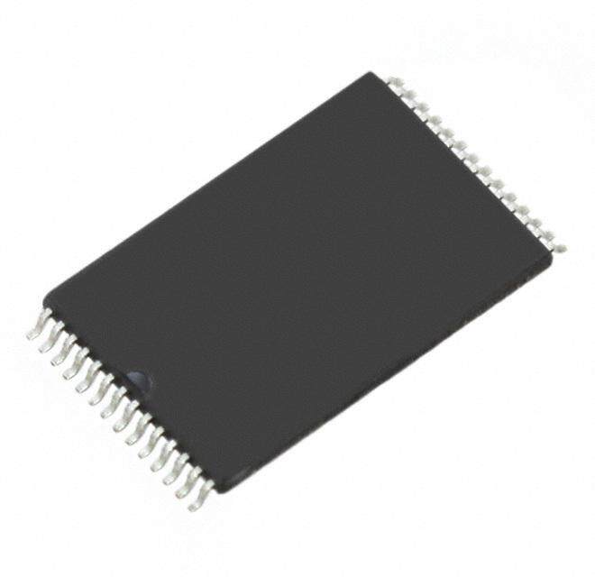
| 描述 | IC EEPROM 64KBIT 150NS 28TSOP电可擦除可编程只读存储器 64K 8K x 8 150 ns 4.5V-5.5V |
| 产品分类 | |
| 品牌 | Atmel |
| 产品手册 | |
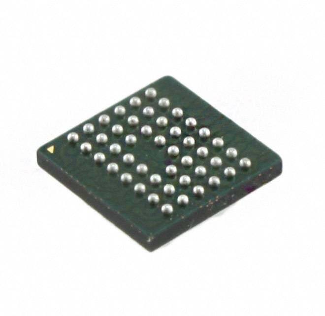
| 产品图片 |
|
| rohs | 符合RoHS无铅 / 符合限制有害物质指令(RoHS)规范要求 |
| 产品系列 | 内存,电可擦除可编程只读存储器,Atmel AT28C64B-15TU- |
| 数据手册 | |
| 产品型号 | AT28C64B-15TU |
| 产品目录页面 | |
| 产品种类 | 电可擦除可编程只读存储器 |
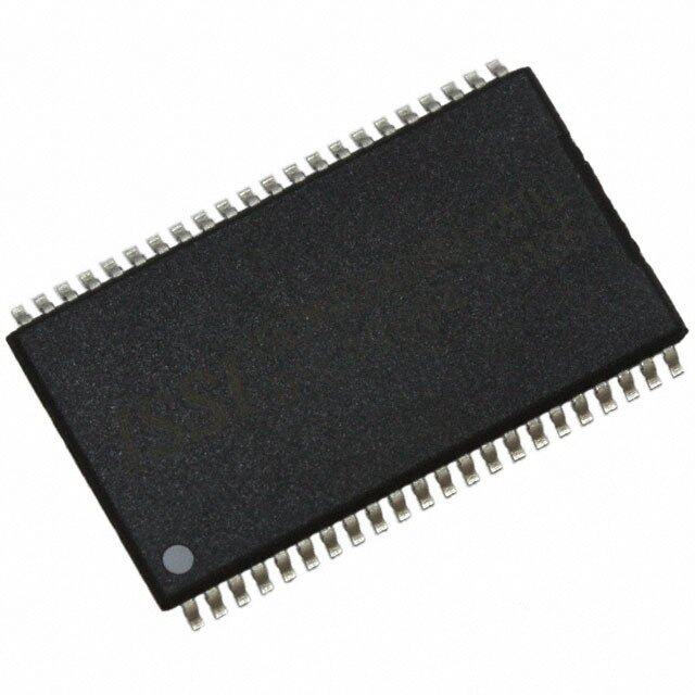
| 供应商器件封装 | 28-TSOP |
| 其它名称 | AT28C64B15TU |
| 包装 | 托盘 |
| 商标 | Atmel |
| 存储器类型 | EEPROM |
| 存储容量 | 64 kbit |
| 安装风格 | SMD/SMT |
| 封装/外壳 | 28-TSSOP (0.465", 11.80mm 宽) |
| 封装/箱体 | TSOP-28 |
| 工作温度 | -40°C ~ 85°C |
| 工作电流 | 40 mA |
| 工作电源电压 | 5 V |
| 工厂包装数量 | 234 |
| 接口 | 并联 |
| 接口类型 | Parallel |
| 数据保留 | 10 yr |
| 最大工作温度 | + 85 C |
| 最大工作电流 | 40 mA |
| 最大时钟频率 | 6.67 MHz |
| 最小工作温度 | - 40 C |
| 标准包装 | 234 |
| 格式-存储器 | EEPROMs - 并行 |
| 电压-电源 | 4.5 V ~ 5.5 V |
| 电源电压-最大 | 5.5 V |
| 电源电压-最小 | 4.5 V |
| 组织 | 8 k x 8 |
| 访问时间 | 150 ns |
| 输出启用访问时间 | 70 ns |
| 速度 | 150ns |


- 商务部:美国ITC正式对集成电路等产品启动337调查
- 曝三星4nm工艺存在良率问题 高通将骁龙8 Gen1或转产台积电
- 太阳诱电将投资9.5亿元在常州建新厂生产MLCC 预计2023年完工
- 英特尔发布欧洲新工厂建设计划 深化IDM 2.0 战略
- 台积电先进制程称霸业界 有大客户加持明年业绩稳了
- 达到5530亿美元!SIA预计今年全球半导体销售额将创下新高
- 英特尔拟将自动驾驶子公司Mobileye上市 估值或超500亿美元
- 三星加码芯片和SET,合并消费电子和移动部门,撤换高东真等 CEO
- 三星电子宣布重大人事变动 还合并消费电子和移动部门
- 海关总署:前11个月进口集成电路产品价值2.52万亿元 增长14.8%


PDF Datasheet 数据手册内容提取
Features • Fast Read Access Time – 150 ns (cid:129) Automatic Page Write Operation – Internal Address and Data Latches for 64 Bytes (cid:129) Fast Write Cycle Times – Page Write Cycle Time: 10 ms Maximum (Standard) 2 ms Maximum (Option – Ref. AT28HC64BF Datasheet) – 1 to 64-byte Page Write Operation (cid:129) Low Power Dissipation 64K (8K x 8) – 40 mA Active Current – 100 µA CMOS Standby Current Parallel (cid:129) Hardware and Software Data Protection (cid:129) DATA Polling and Toggle Bit for End of Write Detection EEPROM with (cid:129) High Reliability CMOS Technology – Endurance: 100,000 Cycles Page Write and – Data Retention: 10 Years (cid:129) Single 5V ±10% Supply Software Data (cid:129) CMOS and TTL Compatible Inputs and Outputs Protection (cid:129) JEDEC Approved Byte-wide Pinout (cid:129) Industrial Temperature Ranges (cid:129) Green (Pb/Halide-free) Packaging Option Only AT28C64B 1. Description The AT28C64B is a high-performance electrically-erasable and programmable read- only memory (EEPROM). Its 64K of memory is organized as 8,192 words by 8 bits. Manufactured with Atmel’s advanced nonvolatile CMOS technology, the device offers access times to 150 ns with power dissipation of just 220 mW. When the device is deselected, the CMOS standby current is less than 100 µA. The AT28C64B is accessed like a Static RAM for the read or write cycle without the need for external components. The device contains a 64-byte page register to allow writing of up to 64 bytes simultaneously. During a write cycle, the addresses and 1 to 64 bytes of data are internally latched, freeing the address and data bus for other operations. Following the initiation of a write cycle, the device will automatically write the latched data using an internal control timer. The end of a write cycle can be detected by DATA POLLING of I/O7. Once the end of a write cycle has been detected, a new access for a read or write can begin. Atmel’s AT28C64B has additional features to ensure high quality and manufacturabil- ity. The device utilizes internal error correction for extended endurance and improved data retention characteristics. An optional software data protection mechanism is available to guard against inadvertent writes. The device also includes an extra 64bytes of EEPROM for device identification or tracking. 0270L–PEEPR–2/09
2. Pin Configurations 2.2 32-lead PLCC Top View Pin Name Function A7 A12 NC DC VCC WE NC A0 - A12 Addresses CE Chip Enable 4 3 2 1 32 31 30 A6 5 29 A8 OE Output Enable A5 6 28 A9 WE Write Enable A4 7 27 A11 A3 8 26 NC I/O0 - I/O7 Data Inputs/Outputs A2 9 25 OE NC No Connect A1 10 24 A10 A0 11 23 CE DC Don’t Connect NC 12 22 I/O7 I/O0 13 21 I/O6 4 5 6 7 8 9 0 1 1 1 1 1 1 2 1 2 D C 3 4 5 O O N D O O O I/ I/ G I/ I/ I/ Note: PLCC package pins 1 and 17 are Don’t Connect. 2.1 28-lead PDIP, 28-lead SOIC Top View 2.3 28-lead TSOP Top View NC 1 28 VCC OE 1 28 A10 A11 2 27 CE A12 2 27 WE A9 3 26 I/O7 A7 3 26 NC A8 4 25 I/O6 A6 4 25 A8 NC 5 24 I/O5 A5 5 24 A9 WE 6 23 I/O4 A4 6 23 A11 VCC 7 22 I/O3 A3 7 22 OE NC 8 21 GND A2 8 21 A10 A12 9 20 I/O2 A1 9 20 CE A7 10 19 I/O1 A0 10 19 I/O7 A6 11 18 I/O0 I/O0 11 18 I/O6 A5 12 17 A0 I/O1 12 17 I/O5 A4 13 16 A1 I/O2 13 16 I/O4 A3 14 15 A2 GND 14 15 I/O3 AT28C64B 2 0270L–PEEPR–2/09
AT28C64B 3. Block Diagram VCC DATA INPUTS/OUTPUTS I/O0 - I/O7 GND OE DATA LATCH OE, CE and WE WE LOGIC INPUT/OUTPUT CE BUFFERS Y DECODER Y-GATING ADDRESS INPUTS CELL MATRIX X DECODER IDENTIFICATION 4. Device Operation 4.1 Read The AT28C64B is accessed like a Static RAM. When CE and OE are low and WE is high, the data stored at the memory location determined by the address pins is asserted on the outputs. The outputs are put in the high-impedance state when either CE or OE is high. This dual line control gives designers flexibility in preventing bus contention in their systems. 4.2 Byte Write A low pulse on the WE or CE input with CE or WE low (respectively) and OE high initiates a write cycle. The address is latched on the falling edge of CE or WE, whichever occurs last. The data is latched by the first rising edge of CE or WE. Once a byte write has been started, it will automati- cally time itself to completion. Once a programming operation has been initiated and for the duration of t , a read operation will effectively be a polling operation. WC 4.3 Page Write The page write operation of the AT28C64B allows 1 to 64 bytes of data to be written into the device during a single internal programming period. A page write operation is initiated in the same manner as a byte write; after the first byte is written, it can then be followed by 1 to 63 additional bytes. Each successive byte must be loaded within 150 µs (t ) of the previous byte. BLC If the t limit is exceeded, the AT28C64B will cease accepting data and commence the internal BLC programming operation. All bytes during a page write operation must reside on the same page as defined by the state of the A6 to A12 inputs. For each WE high to low transition during the page write operation, A6 to A12 must be the same. The A0 to A5 inputs specify which bytes within the page are to be written. The bytes may be loaded in any order and may be altered within the same load period. Only bytes which are spec- ified for writing will be written; unnecessary cycling of other bytes within the page does not occur. 3 0270L–PEEPR–2/09
4.4 DATA Polling The AT28C64B features DATA Polling to indicate the end of a write cycle. During a byte or page write cycle an attempted read of the last byte written will result in the complement of the written data to be presented on I/O7. Once the write cycle has been completed, true data is valid on all outputs, and the next write cycle may begin. DATA Polling may begin at any time during the write cycle. 4.5 Toggle Bit In addition to DATA Polling, the AT28C64B provides another method for determining the end of a write cycle. During the write operation, successive attempts to read data from the device will result in I/O6 toggling between one and zero. Once the write has completed, I/O6 will stop tog- gling, and valid data will be read. Toggle bit reading may begin at any time during the write cycle. 4.6 Data Protection If precautions are not taken, inadvertent writes may occur during transitions of the host system power supply. Atmel® has incorporated both hardware and software features that will protect the memory against inadvertent writes. 4.6.1 Hardware Data Protection Hardware features protect against inadvertent writes to the AT28C64B in the following ways: (a) V sense – if V is below 3.8 V (typical), the write function is inhibited; (b) V power-on delay CC CC CC – once V has reached 3.8V, the device will automatically time out 5 ms (typical) before allow- CC ing a write; (c) write inhibit – holding any one of OE low, CE high, or WE high inhibits write cycles; and (d) noise filter – pulses of less than 15 ns (typical) on the WE or CE inputs will not ini- tiate a write cycle. 4.6.2 Software Data Protection A software controlled data protection feature has been implemented on the AT28C64B. When enabled, the software data protection (SDP), will prevent inadvertent writes. The SDP feature may be enabled or disabled by the user; the AT28C64B is shipped from Atmel with SDP dis- abled. SDP is enabled by the user issuing a series of three write commands in which three specific bytes of data are written to three specific addresses (see “Software Data Protection Algorithms” on page 10). After writing the 3-byte command sequence and waiting t , the entire AT28C64B WC will be protected against inadvertent writes. It should be noted that even after SDP is enabled, the user may still perform a byte or page write to the AT28C64B by preceding the data to be writ- ten by the same 3-byte command sequence used to enable SDP. Once set, SDP remains active unless the disable command sequence is issued. Power transi- tions do not disable SDP, and SDP protects the AT28C64B during power-up and power-down conditions. All command sequences must conform to the page write timing specifications. The data in the enable and disable command sequences is not actually written into the device; their addresses may still be written with user data in either a byte or page write operation. After setting SDP, any attempt to write to the device without the 3-byte command sequence will start the internal write timers. No data will be written to the device. However, for the duration of t , read operations will effectively be polling operations. WC 4.7 Device Identification An extra 64 bytes of EEPROM memory are available to the user for device identification. By rais- ing A9 to 12V ±0.5V and using address locations 1FC0H to 1FFFH, the additional bytes may be written to or read from in the same manner as the regular memory array. AT28C64B 4 0270L–PEEPR–2/09
AT28C64B 5. DC and AC Operating Range AT28C64B-15 Operating Temperature (Case) -40°C - 85°C V Power Supply 5V ±10% CC 6. Operating Modes Mode CE OE WE I/O Read V V V D IL IL IH OUT Write(2) V V V D IL IH IL IN Standby/Write Inhibit V X(1) X High Z IH Write Inhibit X X V IH Write Inhibit X V X IL Output Disable X V X High Z IH Chip Erase V V (3) V High Z IL H IL Notes: 1. X can be V or V . IL IH 2. See “AC Write Waveforms” on page 8. 3. V = 12.0V ±0.5V. H 7. Absolute Maximum Ratings* Temperature Under Bias................................-55°C to +125°C *NOTICE: Stresses beyond those listed under “Absolute Maximum Ratings” may cause permanent dam- Storage Temperature.....................................-65°C to +150°C age to the device. This is a stress rating only and functional operation of the device at these or any All Input Voltages other conditions beyond those indicated in the (including NC Pins) operational sections of this specification is not with Respect to Ground...................................-0.6V to +6.25V implied. Exposure to absolute maximum rating All Output Voltages conditions for extended periods may affect with Respect to Ground.............................-0.6V to V + 0.6V device reliability CC Voltage on OE and A9 with Respect to Ground...................................-0.6V to +13.5V 8. DC Characteristics Symbol Parameter Condition Min Max Units I Input Load Current V = 0V to V + 1V 10 µA LI IN CC I Output Leakage Current V = 0V to V 10 µA LO I/O CC I V Standby Current CMOS CE = V - 0.3V to V + 1V 100 µA SB1 CC CC CC I V Standby Current TTL CE = 2.0V to V + 1V 2 mA SB2 CC CC I V Active Current f = 5 MHz; I = 0 mA 40 mA CC CC OUT V Input Low Voltage 0.8 V IL V Input High Voltage 2.0 V IH V Output Low Voltage I = 2.1 mA 0.40 V OL OL V Output High Voltage I = -400 µA 2.4 V OH OH 5 0270L–PEEPR–2/09
9. AC Read Characteristics AT28C64B-15 Symbol Parameter Min Max Units t Address to Output Delay 150 ns ACC t (1) CE to Output Delay 150 ns CE t (2) OE to Output Delay 0 70 ns OE t (3)(4) CE or OE to Output Float 0 50 ns DF Output Hold from OE, CE or Address, whichever t 0 ns OH occurred first 10. AC Read Waveforms(1)(2)(3)(4) ADDRESS ADDRESS VALID CE t CE t OE OE t DF t OH t ACC HIGH Z OUTPUT OUTPUT VALID Notes: 1. CE may be delayed up to t - t after the address transition without impact on t . ACC CE ACC 2. OE may be delayed up to t - t after the falling edge of CE without impact on t or by t - t after an address change CE OE CE ACC OE without impact on t . ACC 3. t is specified from OE or CE whichever occurs first (C = 5 pF). DF L 4. This parameter is characterized and is not 100% tested. AT28C64B 6 0270L–PEEPR–2/09
AT28C64B 11. Input Test Waveforms and Measurement Level t , t < 5 ns R F 12. Output Test Load 13. Pin Capacitance f = 1 MHz, T = 25°C(1) Symbol Typ Max Units Conditions C 4 6 pF V = 0V IN IN C 8 12 pF V = 0V OUT OUT Note: 1. This parameter is characterized and is not 100% tested. 7 0270L–PEEPR–2/09
14. AC Write Characteristics Symbol Parameter Min Max Units t , t Address, OE Setup Time 0 ns AS OES t Address Hold Time 50 ns AH t Chip Select Setup Time 0 ns CS t Chip Select Hold Time 0 ns CH t Write Pulse Width (WE or CE) 100 ns WP t Data Setup Time 50 ns DS t , t Data, OE Hold Time 0 ns DH OEH 15. AC Write Waveforms 15.1 WE Controlled t OE OES t OEH ADDRESS tAS tCH t CE AH t CS WE t WP t t DS DH DATA IN 15.2 CE Controlled t OE OES t OEH ADDRESS tAS tCH t AH WE t CS CE t WP t t DS DH DATA IN AT28C64B 8 0270L–PEEPR–2/09
AT28C64B 16. Page Mode Characteristics Symbol Parameter Min Max Units t Write Cycle Time 10 ms WC t Write Cycle Time (option available – Ref. AT28HC64BF datasheet) 2 ms WC t Address Setup Time 0 ns AS t Address Hold Time 50 ns AH t Data Setup Time 50 ns DS t Data Hold Time 0 ns DH t Write Pulse Width 100 ns WP t Byte Load Cycle Time 150 µs BLC t Write Pulse Width High 50 ns WPH 17. Page Mode Write Waveforms(1)(2) OE CE t tWPH tBLC WP WE t AS t t DH AH A0 -A12 VALID ADD t DS DATA VALID DATA t WC Notes: 1. A6 through A12 must specify the same page address during each high to low transition of WE (or CE). 2. OE must be high only when WE and CE are both low. 18. Chip Erase Waveforms tS tH tW t = t = 1 µs (min.) S H t = 10 ms (min.) W V = 12.0V ±0.5V H 9 0270L–PEEPR–2/09
19. Software Data Protection Enable 20. Software Data Protection Disable Algorithm(1) Algorithm(1) LOAD DATA AA LOAD DATA AA TO TO ADDRESS 1555 ADDRESS 1555 LOAD DATA 55 LOAD DATA 55 TO TO ADDRESS 0AAA ADDRESS 0AAA LOAD DATA A0 LOAD DATA 80 TO TO ADDRESS 1555 WRITES ENABLED(2) ADDRESS 1555 LOAD DATA XX LOAD DATA AA TO TO ANY ADDRESS(4) ADDRESS 1555 LOAD LAST BYTE LOAD DATA 55 TO TO LAST ADDRESS ENTER DATA ADDRESS 0AAA PROTECT STATE LOAD DATA 20 TO ADDRESS 1555 EXIT DATA Notes: 1. Data Format: I/O7 - I/O0 (Hex); PROTECT STATE(3) LOAD DATA XX Address Format: A12 - A0 (Hex). TO 2. Write Protect state will be activated at end of write ANY ADDRESS(4) even if no other data is loaded. LOAD LAST BYTE 3. Write Protect state will be deactivated at end of write TO LAST ADDRESS period even if no other data is loaded. 4. 1 to 64 bytes of data are loaded. Notes: 1. Data Format: I/O7 - I/O0 (Hex); Address Format: A12 - A0 (Hex). 2. Write Protect state will be activated at end of write even if no other data is loaded. 3. Write Protect state will be deactivated at end of write period even if no other data is loaded. 4. 1 to 64 bytes of data are loaded. 21. Software Protected Write Cycle Waveforms(1)(2) OE CE tWPH tBLC t WP WE t AS t t DH AH A0 -A5 A6 - A12 t DS DATA t WC Notes: 1. A6 through A12 must specify the same page address during each high to low transition of WE (or CE) after the software code has been entered. 2. OE must be high only when WE and CE are both low. AT28C64B 10 0270L–PEEPR–2/09
AT28C64B 22. Data Polling Characteristics(1) Symbol Parameter Min Typ Max Units t Data Hold Time 0 ns DH t OE Hold Time 0 ns OEH t OE to Output Delay(1) ns OE t Write Recovery Time 0 ns WR Notes: 1. These parameters are characterized and not 100% tested. See “AC Read Characteristics” on page 6. 23. Data Polling Waveforms t OEH t DH t WR t OE 24. Toggle Bit Characteristics(1) Symbol Parameter Min Typ Max Units t Data Hold Time 10 ns DH t OE Hold Time 10 ns OEH t OE to Output Delay(2) ns OE t OE High Pulse 150 ns OEHP t Write Recovery Time 0 ns WR Notes: 1. These parameters are characterized and not 100% tested. 2. See “AC Read Characteristics” on page 6. 25. Toggle Bit Waveforms(1)(2)(3) tOEH tOEHP tDH tOE t WR Notes: 1. Toggling either OE or CE or both OE and CE will operate toggle bit. 2. Beginning and ending state of I/O6 will vary. 3. Any address location may be used but the address should not vary. 11 0270L–PEEPR–2/09
26. Normalized I Graphs CC AT28C64B 12 0270L–PEEPR–2/09
AT28C64B 27. Ordering Information 27.1 Green Package Option (Pb/Halide-free) tACC ICC (mA) (ns) Active Standby Ordering Code Package Operation Range AT28C64B-15JU 32J AT28C64B-15SU 28S Industrial 150 40 0.1 AT28C64B-15TU 28T (-40°C to 85°C) AT28C64B-15PU 28P6 27.2 Die Products Contact Atmel Sales for die sales options. Package Type 32J 32-lead, Plastic J-leaded Chip Carrier (PLCC) 28P6 28-lead, 0.600" Wide, Plastic Dual Inline Package (PDIP) 28S 28-lead, 0.300" Wide, Plastic Gull Wing Small Outline (SOIC) 28T 28-lead, Plastic Thin Small Outline Package (TSOP) 13 0270L–PEEPR–2/09
28. Packaging Information 28.1 32J – PLCC 1.14(0.045) X 45˚ PIN NO. 1 1.14(0.045) X 45˚ IDENTIFIER 0.318(0.0125) 0.191(0.0075) E1 E B1 E2 B e A2 D1 A1 D A 0.51(0.020)MAX 45˚ MAX (3X) COMMON DIMENSIONS (Unit of Measure = mm) SYMBOL MIN NOM MAX NOTE D2 A 3.175 – 3.556 A1 1.524 – 2.413 A2 0.381 – – D 12.319 – 12.573 D1 11.354 – 11.506 Note 2 D2 9.906 – 10.922 Notes: 1.This package conforms to JEDEC reference MS-016, Variation AE. E 14.859 – 15.113 2.Dimensions D1 and E1 do not include mold protrusion. Allowable protrusion is .010"(0.254 mm) per side. Dimension D1 E1 13.894 – 14.046 Note 2 and E1 include mold mismatch and are measured at the extreme E2 12.471 – 13.487 material condition at the upper or lower parting line. B 0.660 – 0.813 3. Lead coplanarity is 0.004" (0.102 mm) maximum. B1 0.330 – 0.533 e 1.270 TYP 10/04/01 TITLE DRAWING NO. REV. 2325 Orchard Parkway 32J, 32-lead, Plastic J-leaded Chip Carrier (PLCC) San Jose, CA 95131 32J B R AT28C64B 14 0270L–PEEPR–2/09
AT28C64B 28.2 28P6 – PDIP D PIN 1 E1 A SEATING PLANE A1 L B B1 e E COMMON DIMENSIONS 0º ~ 15º REF (Unit of Measure = mm) C SYMBOL MIN NOM MAX NOTE eB A – – 4.826 A1 0.381 – – D 36.703 – 37.338 Note 2 E 15.240 – 15.875 E1 13.462 – 13.970 Note 2 B 0.356 – 0.559 B1 1.041 – 1.651 Notes: 1.This package conforms to JEDEC reference MS-011, Variation AB. 2.Dimensions D and E1 do not include mold Flash or Protrusion. L 3.048 – 3.556 Mold Flash or Protrusion shall not exceed 0.25 mm (0.010"). C 0.203 – 0.381 eB 15.494 – 17.526 e 2.540 TYP 09/28/01 TITLE DRAWING NO. REV. 2325 Orchard Parkway 28P6, 28-lead (0.600"/15.24 mm Wide) Plastic Dual R San Jose, CA 95131 Inline Package (PDIP) 28P6 B 15 0270L–PEEPR–2/09
28.3 28S – SOIC Dimensions in Millimeters and (Inches). Controlling dimension: Millimeters. 0.51(0.020) 0.33(0.013) 7.60(0.2992) 10.65(0.419) 7.40(0.2914) 10.00(0.394) PIN 1 1.27(0.50) BSC TOP VIEW 18.10(0.7125) 2.65(0.1043) 17.70(0.6969) 2.35(0.0926) 0.30(0.0118) 0.10(0.0040) SIDE VIEWS 0º ~ 8º 0.32(0.0125) 0.23(0.0091) 1.27(0.050) 0.40(0.016) 8/4/03 TITLE DRAWING NO. REV. 2325 Orchard Parkway 28S, 28-lead, 0.300" Body, Plastic Gull Wing Small Outline (SOIC) San Jose, CA 95131 28S B R JEDEC Standard MS-013 AT28C64B 16 0270L–PEEPR–2/09
AT28C64B 28.4 28T – TSOP PIN 1 0º ~ 5º c Pin 1 Identifier Area D1 D L e b L1 E A2 A SEATING PLANE GAGE PLANE COMMON DIMENSIONS A1 (Unit of Measure = mm) SYMBOL MIN NOM MAX NOTE A – – 1.20 A1 0.05 – 0.15 A2 0.90 1.00 1.05 Notes: 1.This package conforms to JEDEC reference MO-183. D 13.20 13.40 13.60 2.Dimensions D1 and E do not include mold protrusion. Allowable D1 11.70 11.80 11.90 Note 2 protrusion on E is 0.15 mm per side and on D1 is 0.25 mm per side. 3. Lead coplanarity is 0.10 mm maximum. E 7.90 8.00 8.10 Note 2 L 0.50 0.60 0.70 L1 0.25 BASIC b 0.17 0.22 0.27 c 0.10 – 0.21 e 0.55 BASIC 12/06/02 TITLE DRAWING NO. REV. 2325 Orchard Parkway 28T, 28-lead (8 x 13.4 mm) Plastic Thin Small Outline San Jose, CA 95131 28T C R Package, Type I (TSOP) 17 0270L–PEEPR–2/09
Headquarters International Atmel Corporation Atmel Asia Atmel Europe Atmel Japan 2325 Orchard Parkway Unit 1-5 & 16, 19/F Le Krebs 9F, Tonetsu Shinkawa Bldg. San Jose, CA 95131 BEA Tower, Millennium City 5 8, Rue Jean-Pierre Timbaud 1-24-8 Shinkawa USA 418 Kwun Tong Road BP 309 Chuo-ku, Tokyo 104-0033 Tel: 1(408) 441-0311 Kwun Tong, Kowloon 78054 Saint-Quentin-en- Japan Fax: 1(408) 487-2600 Hong Kong YvelinesCedex Tel: (81) 3-3523-3551 Tel: (852) 2245-6100 France Fax: (81) 3-3523-7581 Fax: (852) 2722-1369 Tel: (33) 1-30-60-70-00 Fax: (33) 1-30-60-71-11 Product Contact Web Site Technical Support Sales Contact www.atmel.com p_eeprom@atmel.com www.atmel.com/contacts Literature Requests www.atmel.com/literature Disclaimer: The information in this document is provided in connection with Atmel products. No license, express or implied, by estoppel or otherwise,to any intellectualproperty right is granted by this document or in connection with the sale of Atmel products. EXCEPT AS SET FORTH IN ATMEL’S TERMS AND CONDI- TIONS OF SALE LOCATED ON ATMEL’S WEB SITE, ATMEL ASSUMES NO LIABILITY WHATSOEVER AND DISCLAIMS ANY EXPRESS, IMPLIED OR STATUTORY WARRANTY RELATING TO ITS PRODUCTS INCLUDING, BUT NOT LIMITED TO, THE IMPLIED WARRANTY OF MERCHANTABILITY, FITNESS FOR A PARTICULAR PURPOSE, OR NON-INFRINGEMENT. IN NO EVENT SHALL ATMEL BE LIABLE FOR ANY DIRECT, INDIRECT, CONSEQUENTIAL, PUNITIVE, SPECIAL OR INCIDEN- TAL DAMAGES (INCLUDING, WITHOUT LIMITATION, DAMAGES FOR LOSS OF PROFITS, BUSINESS INTERRUPTION, OR LOSS OF INFORMATION) ARISING OUT OF THE USE OR INABILITY TO USE THIS DOCUMENT, EVEN IF ATMEL HAS BEEN ADVISED OF THE POSSIBILITY OF SUCH DAMAGES. Atmel makes no representationsor warranties with respect to the accuracy or completeness of the contents of this document and reserves the right to make changes to specifications and product descriptions at any time without notice. Atmel does not make any commitment to update the information contained herein. Unless specifically provided otherwise, Atmel products are not suitable for, and shall not be used in, automotive applications. Atmel’s products are not intended, authorized, or warranted for use as components in applications intended to support or sustainlife. © 2009 Atmel Corporation. All rights reserved. Atmel®, logo and combinations thereof, and others are registered trademarks or trademarks of Atmel Corporation or its subsidiaries. Other terms and product names may be trademarks of others. 0270L–PEEPR–2/09
Mouser Electronics Authorized Distributor Click to View Pricing, Inventory, Delivery & Lifecycle Information: M icrochip: AT28C64B-20JC AT28C64B-20JI AT28C64B-15JI AT28C64B-15PC AT28C64B-15TC AT28C64B-15TI AT28C64B-15PI AT28C64B-15JC AT28C64B-15SI AT28C64B-15SC AT28C64B-25JI AT28C64B-25SC AT28C64B- 25PC AT28C64B-25JC AT28C64B-15PU AT28C64B-15JU AT28C64B-15SU AT28C64B-15TU AT28C64B-20PC AT28C64B-20PI AT28C64B-20SC AT28C64B-20SI AT28C64B-20TC AT28C64B-20TI AT28C64B-25PI AT28C64B- 25SI AT28C64B-25TC AT28C64B-25TI AT28C64B-15JU-T AT28C64B-15SU-T AT28C64B-15TU-T AT28C64B- 15JU-235