ICGOO在线商城 > ALD110902PAL

 Datasheet下载
- 型号: ALD110902PAL
- 制造商: Advanced Linear Devices
- 库位|库存: xxxx|xxxx
- 要求:
| 数量阶梯 | 香港交货 | 国内含税 |
| +xxxx | $xxxx | ¥xxxx |
查看当月历史价格
查看今年历史价格
ALD110902PAL产品简介:
ICGOO电子元器件商城为您提供ALD110902PAL由Advanced Linear Devices设计生产,在icgoo商城现货销售,并且可以通过原厂、代理商等渠道进行代购。 提供ALD110902PAL价格参考以及Advanced Linear DevicesALD110902PAL封装/规格参数等产品信息。 你可以下载ALD110902PAL参考资料、Datasheet数据手册功能说明书, 资料中有ALD110902PAL详细功能的应用电路图电压和使用方法及教程。
| 参数 | 数值 |
| 产品目录 | |
| ChannelMode | Depletion |
| 描述 | MOSFET 2N-CH 10.6V 8DIPMOSFET Dual EPAD(R) N-Ch |
| 产品分类 | FET - 阵列分离式半导体 |
| FET功能 | 标准 |
| FET类型 | 2 N 沟道(双)配对 |
| Id-ContinuousDrainCurrent | 12 mA |
| Id-连续漏极电流 | 12 mA |
| 品牌 | Advanced Linear Devices Inc |
| 产品手册 | |
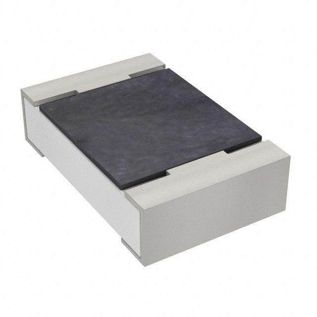
| 产品图片 |
|
| rohs | 符合RoHS无铅 / 符合限制有害物质指令(RoHS)规范要求 |
| 产品系列 | 晶体管,MOSFET,Advanced Linear Devices ALD110902PALEPAD® |
| mouser_ship_limit | 根据美国政府的出口法规规定,Mouser无法将此产品销售到您所在的国家。 |
| 数据手册 | |
| 产品型号 | ALD110902PAL |
| Pd-PowerDissipation | 500 mW |
| Pd-功率耗散 | 500 mW |
| RdsOn-Drain-SourceResistance | 500 Ohms |
| RdsOn-漏源导通电阻 | 500 Ohms |
| Vds-Drain-SourceBreakdownVoltage | 10 V |
| Vds-漏源极击穿电压 | 10 V |
| Vgs-Gate-SourceBreakdownVoltage | 10.6 V |
| Vgs-栅源极击穿电压 | 10.6 V |
| 不同Id时的Vgs(th)(最大值) | 220mV @ 1µA |
| 不同Vds时的输入电容(Ciss) | 2.5pF @ 5V |
| 不同Vgs时的栅极电荷(Qg) | - |
| 不同 Id、Vgs时的 RdsOn(最大值) | 500 欧姆 @ 4.2V |
| 产品种类 | MOSFET |
| 供应商器件封装 | 8-PDIP |
| 其它名称 | 1014-1034 |
| 典型关闭延迟时间 | 10 ns |
| 功率-最大值 | 500mW |
| 包装 | 管件 |
| 商标 | Advanced Linear Devices |
| 安装类型 | 通孔 |
| 安装风格 | Through Hole |
| 导通电阻 | 500 Ohms |
| 封装/外壳 | 8-DIP(0.300",7.62mm) |
| 封装/箱体 | PDIP-8 |
| 工厂包装数量 | 50 |
| 晶体管极性 | N-Channel |
| 最大工作温度 | + 70 C |
| 最小工作温度 | 0 C |
| 标准包装 | 50 |
| 正向跨导-最小值 | 0.0014 S |
| 汲极/源极击穿电压 | 10 V |
| 漏极连续电流 | 12 mA |
| 漏源极电压(Vdss) | 10.6V |
| 电流-连续漏极(Id)(25°C时) | - |
| 系列 | ALD110902P |
| 通道模式 | Depletion |
| 配置 | Dual |


- 商务部:美国ITC正式对集成电路等产品启动337调查
- 曝三星4nm工艺存在良率问题 高通将骁龙8 Gen1或转产台积电
- 太阳诱电将投资9.5亿元在常州建新厂生产MLCC 预计2023年完工
- 英特尔发布欧洲新工厂建设计划 深化IDM 2.0 战略
- 台积电先进制程称霸业界 有大客户加持明年业绩稳了
- 达到5530亿美元!SIA预计今年全球半导体销售额将创下新高
- 英特尔拟将自动驾驶子公司Mobileye上市 估值或超500亿美元
- 三星加码芯片和SET,合并消费电子和移动部门,撤换高东真等 CEO
- 三星电子宣布重大人事变动 还合并消费电子和移动部门
- 海关总署:前11个月进口集成电路产品价值2.52万亿元 增长14.8%


PDF Datasheet 数据手册内容提取
e ADVANCED TM LINEAR EPEANDA®BLED DEVICES, INC. ALD110802/ALD110902 QUAD/DUAL N-CHANNEL ENHANCEMENT MODE EPAD® PRECISION MATCHED PAIR MOSFET ARRAY VGS(th)= +0.20V GENERAL DESCRIPTION APPLICATIONS ALD110802/ALD110902 are high precision monolithic quad/dual enhance- • Ultra low power (nanowatt) analog and digital ment mode N-Channel MOSFETS matched at the factory using ALD’s circuits proven EPAD® CMOS technology. These devices are intended for low volt- • Ultra low operating voltage (<0.20V) circuits age, small signal applications. The ALD110802/ALD110902 MOSFETS are • Sub-threshold biased and operated circuits designed and built for exceptional device electrical characteristics match- • Precision current mirrors and current sources ing. Since these devices are on the same monolithic chip, they also exhibit • Nano-Amp current sources excellent tempco tracking characteristics. They are versatile circuit elements • High impedance resistor simulators useful as design components for a broad range of analog applications, • Capacitive probes and sensor interfaces such as basic building blocks for current sources, differential amplifier input • Differential amplifier input stages stages, transmission gates, and multiplexer applications. For most applica- • Discrete Voltage comparators and level shifters tions, connect the V+ pin to the most positive voltage and the V- and IC • Voltage bias circuits pins to the most negative voltage in the system. All other pins must have • Sample and Hold circuits voltages within these voltage limits at all times. • Analog and digital inverters • Charge detectors and charge integrators The ALD110802/ALD110902 devices are built for minimum offset voltage • Source followers and High Impedance buffers and differential thermal response, and they are suited for switching and • Current multipliers amplifying applications in <+0.1V to +10V systems where low input bias • Discrete Analog switches / multiplexers current, low input capacitance and fast switching speed are desired, as these devices exhibit well controlled turn-off and sub-threshold character- istics and can be biased and operated in the sub-threshold region. Since PIN CONFIGURATION these are MOSFET devices, they feature very large (almost infinite) cur- rent gain in a low frequency, or near DC, operating environment. ALD110802 The ALD110802/ALD110902 are suitable for use in very low operating volt- age or very low power (nanowatt), precision applications which require very V- V- IC* 1 16 IC* high current gain, beta, such as current mirrors and current sources. The high input impedance and the high DC current gain of the Field Effect Tran- GN1 2 15 GN2 sistors result from extremely low current loss through the control gate. The M 1 M 2 DC current gain is limited by the gate input leakage current, which is speci- DN1 3 14 DN2 fied at 30pA at room temperature. For example, DC beta of the device at a S12 4 V+ 13 V+ drain current of 3mA, input leakage current of 30pA, and 25°C is 3mA/30pA = 100,000,000. V- 5 V- 12 S34 FEATURES DN4 6 M 4 M 3 11 DN3 • Enhancement-mode (normally off) GN4 7 10 GN3 • Precision Gate Threshold Voltage of +0.20V IC* 8 9 IC* • Matched MOSFET-to-MOSFET characteristics V- V- • Tight lot-to-lot parametric control • Low input capacitance SCL, PCL PACKAGES • VGS(th) match (VOS) to 10mV • High input impedance — 1012Ω typical ALD110902 • Positive, zero, and negative VGS(th) temperature coefficient • DC current gain >108 V- V- • Low input and output leakage currents IC* 1 8 IC* GN1 2 7 GN2 ORDERING INFORMATION (“L” suffix denotes lead-free (RoHS)) M 1 M 2 DN1 3 6 DN2 Operating Temperature Range* 0°C to +70°C 0°C to +70°C S12 4 V- 5 V- 16-Pin 16-Pin 8-Pin 8-Pin SOIC Plastic Dip SOIC Plastic Dip SAL, PAL PACKAGES Package Package Package Package *IC pins are internally connected. Connect to V- ALD110802SCL ALD110802PCL ALD110902SAL ALD110902PAL * Contact factory for industrial temp. range or user-specified threshold voltage values. ©2016 Advanced Linear Devices, Inc., Vers. 2.3 www.aldinc.com 1 of 12
ABSOLUTE MAXIMUM RATINGS Drain-Source voltage, VDS 10.6V Gate-Source voltage, VGS 10.6V Power dissipation 500 mW Operating temperature range SCL, PCL, SAL, PAL 0°C to +70°C Storage temperature range -65°C to +150°C Lead temperature, 10 seconds +260°C CAUTION: ESD Sensitive Device. Use static control procedures in ESD controlled environment. OPERATING ELECTRICAL CHARACTERISTICS V+ = +5V V- = GND TA = 25°C unless otherwise specified ALD110802/ALD110902 Parameter Symbol Min Typ Max Unit Test Conditions Gate Threshold Voltage VGS(th) 0.18 0.20 0.22 V IDS = 1µA, VDS = 0.1V Offset Voltage VOS 2 10 mV VGS(th)1-VGS(th)2 Offset VoltageTempco TCVOS 5 µV/ °C VDS1 = VDS2 Gate Threshold Voltage TCVGS(th) -1.7 mV/ °C IDS = 1µA, VDS = 0.1V Tempco 0.0 IDS = 20µA, VDS = 0.1V +1.6 IDS = 40µA, VDS = 0.1V Drain Source On Current IDS(ON) 12.0 mA VGS = +9.7V, VDS = +5V 3.0 VGS = +4.2V, VDS = +5V Forward Transconductance GFS 1.4 mmho VGS = +4.2V VDS = +9.2V Transconductance Mismatch ∆GFS 1.8 % Output Conductance GOS 68 µmho VGS = +4.2V VDS = +9.2V Drain Source On Resistance RDS(ON) 500 Ω VGS = +4.2V VDS = +0.1V Drain Source On Resistance ∆RDS(ON) 0.5 % Mismatch Drain Source Breakdown BVDSX 10 V V- = VGS = -0.8V Voltage IDS = 1.0µA Drain Source Leakage Current1 IDS(OFF) 10 400 pA VGS = -0.8V, VDS =+5V V- = -5V 4 nA TA = 125°C Gate Leakage Current1 IGSS 3 200 pA VGS = +5V, VDS = 0V 1 nA TA =125°C Input Capacitance CISS 2.5 pF Transfer Reverse Capacitance CRSS 0.1 pF Turn-on Delay Time ton 10 ns V+ = 5V, RL= 5KΩ Turn-off Delay Time toff 10 ns V+ = 5V, RL= 5KΩ Crosstalk 60 dB f = 100KHz Notes: 1 Consists of junction leakage currents ALD110802/ALD110902, Vers. 2.3 Advanced Linear Devices 2 of 12
PERFORMANCE CHARACTERISTICS OF EPAD® PRECISION MATCHED PAIR MOSFET FAMILY ALD1108xx/ALD1109xx/ALD1148xx/ALD1149xx are monolithic signal voltages are applied to the gate terminal, the designer/user quad/dual N-Channel MOSFETs matched at the factory using ALD’s can depend on the EPAD MOSFET device to be controlled, modu- proven EPAD® CMOS technology. These devices are intended for lated and turned off precisely. The device can be modulated and low voltage, small signal applications. turned-off under the control of the gate voltage in the same manner as the enhancement mode EPAD MOSFET and the same device ALD’s Electrically Programmable Analog Device (EPAD) technol- equations apply. ogy provides a family of matched transistors with a range of preci- sion threshold values. All members of this family are designed and EPAD MOSFETs are ideal for minimum offset voltage and differen- actively programmed for exceptional matching of device electrical tial thermal response, and they are used for switching and amplify- characteristics. Threshold values range from -3.50V Depletion to ing applications in low voltage (1V to 10V or +/-0.5V to +/-5V) or +3.50V Enhancement devices, including standard products speci- ultra low voltage (less than 1V or +/-0.5V) systems. They feature fied at -3.50V, -1.30V, -0.40V, +0.00V, +0.20V, +0.40V, +0.80V, low input bias current (less than 30pA max.), ultra low power +1.40V, and +3.30V. ALD can also provide any customer desired (microWatt) or Nanopower (power measured in nanoWatt) opera- value between -3.50V and +3.50V. For all these devices, even the tion, low input capacitance and fast switching speed. These de- depletion and zero threshold transistors, ALD EPAD technology vices can be used where a combination of these characteristics enables the same well controlled turn-off, subthreshold, and low are desired. leakage characteristics as standard enhancement mode MOSFETs. With the design and active programming, even units from different batches and different dates of manufacture have well matched char- KEY APPLICATION ENVIRONMENT acteristics. As these devices are on the same monolithic chip, they also exhibit excellent tempco tracking. EPAD MOSFET Array products are for circuit applications in one or more of the following operating environments: This EPAD MOSFET Array product family (EPAD MOSFET) is avail- * Low voltage: 1V to 10V or +/-0.5V to +/-5V able in the three separate categories, each providing a distinctly * Ultra low voltage: less than 1V or +/-0.5V different set of electrical specifications and characteristics. The first * Low power: voltage x current = power measured in microwatt category is the ALD110800/ALD110900 Zero-Threshold™ mode * Nanopower: voltage x current = power measured in nanowatt EPAD MOSFETs. The second category is the ALD1108xx/ * Precision matching and tracking of two or more MOSFETs ALD1109xx enhancement mode EPAD MOSFETs. The third cat- egory is the ALD1148xx/ALD1149xx depletion mode EPAD MOSFETs. (The suffix “xx” denotes threshold voltage in 0.1V steps, ELECTRICAL CHARACTERISTICS for example, xx = 08 denotes 0.80V). The turn-on and turn-off electrical characteristics of the EPAD The ALD110800/ALD110900 (quad/dual) are EPAD MOSFETs in MOSFET products are shown in the Drain-Source On Current vs which the individual threshold voltage of each MOSFET is fixed at Drain-Source On Voltage and Drain-Source On Current vs Gate- zero. The threshold voltage is defined as IDS = 1µA @ VDS = 0.1V Source Voltage graphs. Each graph shows the Drain-Source On when the gate voltage VGS = 0.00V. Zero threshold devices oper- Current versus Drain-Source On Voltage characteristics as a func- ate in the enhancement region when operated above threshold volt- tion of Gate-Source voltage in a different operating region under age and current level (VGS > 0.00V and IDS > 1µA) and subthresh- different bias conditions. As the threshold voltage is tightly speci- old region when operated at or below threshold voltage and cur- fied, the Drain-Source On Current at a given gate input voltage is rent level (VGS <= 0.00V and IDS < 1µA). This device, along with better controlled and more predictable when compared to many other very low threshold voltage members of the product family, other types of MOSFETs. constitute a class of EPAD MOSFETs that enable ultra low supply voltage operation and nanopower type of circuit designs, applicable EPAD MOSFETs behave similarly to a standard MOSFET, there- in either analog or digital circuits. fore classic equations for a n-channel MOSFET applies to EPAD MOSFET as well. The Drain current in the linear region (VDS < The ALD1108xx/ALD1109xx (quad/dual) product family features VGS - VGS(th)) is given by: precision matched enhancement mode EPAD MOSFET devices, which require a positive bias voltage to turn on. Precision threshold IDS = u . COX . W/L . [VGS - VGS(th) - VDS/2] . VDS values such as +1.40V, +0.80V, +0.20V are offered. No conductive channel exists between the source and drain at zero applied gate where: u = Mobility voltage for these devices, except that the +0.20V version has a COX = Capacitance / unit area of Gate electrode subthreshold current at about 20nA. VGS = Gate to Source voltage VGS(th) = Turn-on threshold voltage The ALD1148xx/ALD1149xx (quad/dual) features depletion mode VDS = Drain to Source voltage EPAD MOSFETs, which are normally-on devices when the gate W = Channel width bias voltage is at zero volts. The depletion mode threshold voltage L = Channel length is at a negative voltage level at which the EPAD MOSFET turns off. Without a supply voltage and/or with VGS = 0.0V the EPAD MOSFET In this region of operation the IDS value is proportional to VDS value device is already turned on and exhibits a defined and controlled and the device can be used as a gate-voltage controlled resistor. on-resistance between the source and drain terminals. For higher values of VDS where VDS >= VGS - VGS(th), the satura- The ALD1148xx/ALD1149xx depletion mode EPAD MOSFETs are tion current IDS is now given by (approx.): different from most other types of depletion mode MOSFETs and certain types of JFETs in that they do not exhibit high gate leakage IDS = u . COX . W/L . [VGS - VGS(th)]2 currents and channel/junction leakage currents. When negative ALD110802/ALD110902, Vers. 2.3 Advanced Linear Devices 3 of 12
PERFORMANCE CHARACTERISTICS OF EPAD® PRECISION MATCHED PAIR MOSFET FAMILY (cont.) SUB-THRESHOLD REGION OF OPERATION ZERO TEMPERATURE COEFFICIENT (ZTC) OPERATION Low voltage systems, namely those operating at 5V, 3.3V or less, For an EPAD MOSFET in this product family, there exist operating typically require MOSFETs that have threshold voltage of 1V or points where the various factors that cause the current to increase less. The threshold, or turn-on, voltage of the MOSFET is a voltage as a function of temperature balance out those that cause the cur- below which the MOSFET conduction channel rapidly turns off. For rent to decrease, thereby canceling each other, and resulting in net analog designs, this threshold voltage directly affects the operating temperature coefficient of near zero. One of these temperature signal voltage range and the operating bias current levels. stable operating points is obtained by a ZTC voltage bias condi- tion, which is 0.55V above a threshold voltage when VGS = VDS, At or below threshold voltage, an EPAD MOSFET exhibits a turn- resulting in a temperature stable current level of about 68µA. For off characteristic in an operating region called the subthreshold re- other ZTC operating points, see ZTC characteristics. gion. This is when the EPAD MOSFET conduction channel rapidly turns off as a function of decreasing applied gate voltage. The con- duction channel induced by the gate voltage on the gate electrode PERFORMANCE CHARACTERISTICS decreases exponentially and causes the drain current to decrease exponentially. However, the conduction channel does not shut off Performance characteristics of the EPAD MOSFET product family abruptly with decreasing gate voltage. Rather, it decreases at a are shown in the following graphs. In general, the threshold voltage fixed rate of approximately 116mV per decade of drain current de- shift for each member of the product family causes other affected crease. Thus, if the threshold voltage is +0.20V, for example, the electrical characteristics to shift with an equivalent linear shift in drain current is 1µA at VGS = +0.20V. At VGS = +0.09V, the drain VGS(th) bias voltage. This linear shift in VGS causes the subthresh- current would decrease to 0.1µA. Extrapolating from this, the drain old I-V curves to shift linearly as well. Accordingly, the subthreshold current is 0.01µA (10nA) at VGS = -0.03V, 1nA at VGS = -0.14V, operating current can be determined by calculating the gate volt- and so forth. This subthreshold characteristic extends all the way age drop relative to its threshold voltage, VGS(th). down to current levels below 1nA and is limited by other currents such as junction leakage currents. RDS(ON) AT VGS = GROUND At a drain current to be declared “zero current” by the user, the VGS voltage at that zero current can now be estimated. Note that Several of the EPAD MOSFETs produce a fixed resistance when using the above example, with VGS(th) = +0.20V, the drain current their gate is grounded. For ALD110800, the drain current is 1µA at still hovers around 20nA when the gate is at zero volts, or ground. VDS = 0.1V and VGS = 0.0V. Thus, just by grounding the gate of the ALD110800, a resistor with RDS(ON) = ~100KΩ is produced. When an ALD114804 gate is grounded, the drain current IDS = LOW POWER AND NANOPOWER 18.5µA @ VDS = 0.1V, producing RDS(ON) = 5.4KΩ. Similarly, ALD114813 and ALD114835 produce drain currents of 77µA and When supply voltages decrease, the power consumption of a given 185µA, respectively, at VGS = 0.0V, and RDS(ON) values of 1.3KΩ load resistor decreases as the square of the supply voltage. So and 540Ω, respectively. one of the benefits in reducing supply voltage is to reduce power consumption. While decreasing power supply voltages and power consumption go hand-in-hand with decreasing useful AC bandwidth MATCHING CHARACTERISTICS and at the same time increases noise effects in the circuit, a circuit designer can make the necessary tradeoffs and adjustments in any A key benefit of using a matched pair EPAD MOSFET is to main- given circuit design and bias the circuit accordingly. tain temperature tracking. In general, for EPAD MOSFET matched pair devices, one device of the matched pair has gate leakage cur- With EPAD MOSFETs, a circuit that performs a specific function rents, junction temperature effects, and drain current temperature can be designed so that power consumption can be minimized. In coefficient as a function of bias voltage that cancel out similar ef- some cases, these circuits operate in low power mode where the fects of the other device, resulting in a temperature stable circuit. power consumed is measure in micro-watts. In other cases, power As mentioned earlier, this temperature stability can be further en- dissipation can be reduced to the nano-watt region and still provide hanced by biasing the matched-pairs at Zero Tempco (ZTC) point, a useful and controlled circuit function operation. even though that could require special circuit configuration and power consumption design consideration. ALD110802/ALD110902, Vers. 2.3 Advanced Linear Devices 4 of 12
TYPICAL PERFORMANCE CHARACTERISTICS OUTPUT CHARACTERISTICS DRAIN-SOURCE ON RESISTANCE vs. DRAIN-SOURCE ON CURRENT 5 E 2500 NT TA = +25°C VGS - VGS(th) = +5V NC TA = +25°C RE 4 TA 2000 R S CU VGS - VGS(th) = +4V ESI N 3 R 1500 RCE O (mA) 2 VGS - VGS(th) = +3V CE ON ()Ω 1000 VGS = VGS(th) + 4V U R O U S VGS - VGS(th) = +2V O AIN- 1 N-S 500 DR VGS - VGS(th) = +1V RAI VGS = VGS(th) + 6V 0 D 0 0 2 4 6 8 10 10 100 1000 10000 DRAIN-SOURCE ON VOLTAGE (V) DRAIN-SOURCE ON CURRENT (µA) FORWARD TRANSFER CHARACTERISTICS TRANSCONDUCTANCE vs. AMBIENT TEMPERATURE 20 2.5 T REN VTDAS = = + +2150°CV VGS(th) = -3.5V E 2.0 CUR 15 VGS(th) = -1.3V ANC URCE ON (mA) 10 VGS(thV) G= S0(.t0hV) = -0.4V CONDUCT (mA/V) 11..50 SO VGS(th) = +0.2V NS AIN- 5 VGS(th) = +0.8V TRA 0.5 R D 0 VGS(th) = +1.4V 0 -4 -2 0 2 4 6 8 10 -50 -25 0 25 50 75 100 125 GATE-SOURCE VOLTAGE (V) AMBIENT TEMPERATURE (°C) SUBTHRESHOLD FORWARD TRANSFER SUBTHRESHOLD FORWARD TRANSFER CHARACTERISTICS CHARACTERISTICS 100000 10000 URRENT 110000000 VTAD S= =+ 2+50°.1CV URRENT 1000 SVlDoSp e= =~+ 01.110VmV/decade C C 100 SOURCE ON (nA) 1 01 010 VGS= (t-h3.) 5V VGS= (t-h1.) 3V VGS= (t-h0.) 4VVGS= (t0.h)0 V VG S= (t+h0).2V VGS= (t+h0). 8V VGS= (t+h1). 4V SOURCE ON (nA) 1 01 N- N- AI 0.1 AI 0.1 R R D D 0.01 0.01 -4 -3 -2 -1 0 1 2 VGS(th)-0.5 VGS(th)-0.4 VGS(th)-0.3 VGS(th)-0.2 VGS(th)-0.1 VGS(th) GATE-SOURCE VOLTAGE (V) GATE-SOURCE VOLTAGE (V) ALD110802/ALD110902, Vers. 2.3 Advanced Linear Devices 5 of 12
TYPICAL PERFORMANCE CHARACTERISTICS (cont.) DRAIN-SOURCE ON CURRENT, BIAS DRAIN-SOURCE ON CURRENT, BIAS CURRENT vs. AMBIENT TEMPERATURE CURRENT vs. AMBIENT TEMPERATURE 5 100 NT NT Zero Temperature RE 4 -55°C RE Coefficient (ZTC) R R U -25°C U N C 3 N C +125°C RCE O (mA) 2 0°C RCE O(A)µ 50 U U O O S S N- 1 N- RAI RAI -25°C D +70°C +125°C D 0 0 VGS(th)-1 VGS(th) VGS(th)+1 VGS(th)+2 VGS(th)+3 VGS(th)+4 VGS(th) VGS(th)+0.2 VGS(th)+0.4 VGS(th)+0.6 VGS(th)+0.8 VGS(th)+1.0 GATE- AND DRAIN-SOURCE VOLTAGE GATE- AND DRAIN-SOURCE VOLTAGE (VGS = VDS) (V) (VGS = VDS) (V) DRAIN-SOURCE ON CURRENT vs. GATE-SOURCE VOLTAGE vs. DRAIN-SOURCE ON RESISTANCE DRAIN-SOURCE ON CURRENT 100000 VGS(th)+4 OURCE ON CURRENT(A)µ 110010 0001 01000 VDS = +0.1V TVAG S= =+ 2-45.°0CVVVDD tSSo = =+ ++551.4V0VV OURCE VOLTAGE (V) VVVGGGSSS(((ttthhh)))+++231 VVDGSS =S DROVNIDD S•S (IODNS)(ON)VTAD S=VT =AD+ 2 S+=50 =°+.C5 1+V205.5°CV VTAD S= =+ 1+255V°C AIN-S 0.1 VDS = +1V TE-S VGS(th) VTAD S= =+ 2+55°VC R A D G 0.01 VGS(th)-1 0.1 1 10 100 1000 10000 0.1 1 10 100 1000 10000 DRAIN-SOURCE ON RESISTANCE (KΩ) DRAIN-SOURCE ON CURRENT (µA) DRAIN-SOURCE ON CURRENT OFFSET VOLTAGE vs. vs. OUTPUT VOLTAGE AMBIENT TEMPERATURE 5 4 T EN VDS = +10V 3 N CURR 43 TA = +25°C LTAGE 12 REPRESENTATIVE UNITS OURCE O (mA) 2 VDS = +5V FFSET VO(mV) -01 S O -2 N- 1 VDS = +1V AI -3 R D 0 -4 VGS(th) VGS(th)+1 VGS(th)+2 VGS(th)+3 VGS(th)+4 VGS(th)+5 -50 -25 0 25 50 75 100 125 OUTPUT VOLTAGE (V) AMBIENT TEMPERATURE (°C) ALD110802/ALD110902, Vers. 2.3 Advanced Linear Devices 6 of 12
TYPICAL PERFORMANCE CHARACTERISTICS (cont.) GATE LEAKAGE CURRENT GATE SOURCE VOLTAGE vs. vs. AMBIENT TEMPERATURE DRAIN-SOURCE ON RESISTANCE 10000 VGS(th)+4 ENT 1000 E (V) 0.0V ≤ VDS ≤ 5.0V R G VGS(th)+3 +125°C UR 100 TA D VDS C L KAGE (pA) 10 CE VO VGS(th)+2 +25°C VGS IDS(ON) A R LE 1 OU S GATE 0.1 IGSS ATE-S VGS(th)+1 G 0.01 VGS(th) -50 -25 0 25 50 75 100 125 0 2 4 6 8 10 AMBIENT TEMPERATURE (°C) DRAIN-SOURCE ON RESISTANCE (KΩ) DRAIN-GATE DIODE CONNECTED VOLTAGE TRANSFER CHARACTERISTICS TEMPCO vs. DRAIN-SOURCE ON CURRENT D 5 1.6 CONNECTEO (mV/C)° 2.5 -55°C ≤ TA ≤ +125°C CTANCE 1.2 VTDAS = = + +2150°CV VGS(th) = -0VV.4GGVSS((tthh)) == --31..53VV E DIODE E TEMPC 0 SCONDU(m)-1Ω 0.8 TG N GATA -2.5 RA 0.4 VGS(th) = 0.0V N-OL T VGS(th) = +0.2V AIV VGS(th) = +0.8V DR -5 0.0 VGS(th) = +1.4V 1 10 100 1000 -4 -2 0 2 4 6 8 10 DRAIN-SOURCE ON CURRENT (µA) GATE-SOURCE VOLTAGE (V) ZERO TEMPERATURE SUBTHRESHOLD CHARACTERISTICS COEFFICIENT CHARACTERISTICS 0.6 2.5 VGS(th) = -3.5V GE E 2.0 A G T 0.5 A OL VGS(th) = -1.3V, -0.4V, 0.0V, +0.2V, +0.8V, +1.4V LT 1.5 TE-SOURCE V(V) 00..32 E-SOURCE VO(V) 01..50 VTAG S=( +th2)5 =° C+0VT.4AGV S=( +th5)5 =° C+0.4V GA AT 0.0 0.0 G -0.5 VTAG S=( +th2)5 =° C+0.2V VTAG S=( +th5)5 =° C+0.2V 0.1 0.2 0.5 1.0 2.0 5.0 100000 10000 1000 100 10 1 0.1 DRAIN-SOURCE ON VOLTAGE (V) DRAIN-SOURCE ON CURRENT (nA) ALD110802/ALD110902, Vers. 2.3 Advanced Linear Devices 7 of 12
TYPICAL PERFORMANCE CHARACTERISTICS (cont.) TRANCONDUCTANCE vs. THRESHOLD VOLTAGE vs. DRAIN-SOURCE ON CURRENT AMBIENT TEMPERATURE 1.2 4.0 TA = +25°C NCE 0.9 VDS = +10V TAGE 3.0 IVDDSS = = + +10µ.A1V A O NDUCTm)-1Ω 0.6 OLD V(V) 2.0 TARNCO( 0.3 THRESH 1.0 Vt = 0.0V VVtt == ++10..48VV Vt = +0.2V Vt = +0.4V 0.0 0.0 0 2 4 6 8 10 -50 -25 0 25 50 75 100 125 DRAIN-SOURCE ON CURRENT (mA) AMBIENT TEMPERATURE (°C) NORMALIZED SUBTHRESHOLD CHARACTERISTICS RELATIVE TO SUBTHRESHOLD FORWARD GATE THRESHOLD VOLTAGE TRANSFER CHARACTERISTICS 0.3 2.0 RCE VOLTAGEV (V)GS(th) -000...0211 VDS = +0.1V OLD VOLTAGE(V) -101...000 IVDDSS = = + +10µ.A1V VVGGSS(t(hth) )= = - 00..40VV E-SOUV- GS -0.2 +25°C RESH -2.0 VGS(th) = -1.3V T H GA -0.3 +55°C T -3.0 VGS(th) = -3.5V -0.4 -4.0 10000 1000 100 10 1 0.1 -25 25 75 125 DRAIN-SOURCE ON CURRENT (nA) AMBIENT TEMPERATURE (°C) ALD110802/ALD110902, Vers. 2.3 Advanced Linear Devices 8 of 12
SOIC-16 PACKAGE DRAWING 16 Pin Plastic SOIC Package E Millimeters Inches Dim Min Max Min Max A 1.35 1.75 0.053 0.069 S (45°) A1 0.10 0.25 0.004 0.010 b 0.35 0.45 0.014 0.018 C 0.18 0.25 0.007 0.010 D-16 9.80 10.00 0.385 0.394 E 3.50 4.05 0.140 0.160 D e 1.27 BSC (cid:31) 0.050 BSC H 5.70 6.30 0.224 0.248 L 0.60 0.937 0.024 0.037 A ø 0° 8° 0° 8° e A1 S 0.25 0.50 0.010 0.020 b (cid:31) S (45°) H C L ø ALD110802/ALD110902, Vers. 2.3 Advanced Linear Devices 9 of 12
PDIP-16 PACKAGE DRAWING 16 Pin Plastic DIP Package E E1 Millimeters Inches Dim Min Max Min Max A 3.81 5.08 0.105 0.200 A1 0.38 1.27 0.015 0.050 A2 1.27 2.03 0.050 0.080 b 0.89 1.65 0.035 0.065 b1 0.38 0.51 0.015 0.020 c 0.20 0.30 0.008 0.012 D D-16 18.93 21.33 0.745 0.840 S E 5.59 7.11 0.220 0.280 E1 7.62 8.26 0.300 0.325 A2 e 2.29 2.79 0.090 0.110 A e1 7.37 7.87 0.290 0.310 A1 L L 2.79 3.81 0.110 0.150 b e S-16 0.38 1.52 0.015 0.060 ø 0° 15° 0° 15° b1 c e1 ø ALD110802/ALD110902, Vers. 2.3 Advanced Linear Devices 10 of 12
SOIC-8 PACKAGE DRAWING 8 Pin Plastic SOIC Package E Millimeters Inches Dim Min Max Min Max A 1.35 1.75 0.053 0.069 S (45°) A1 0.10 0.25 0.004 0.010 b 0.35 0.45 0.014 0.018 C 0.18 0.25 0.007 0.010 D-8 4.69 5.00 0.185 0.196 D E 3.50 4.05 0.140 0.160 e 1.27 BSC 0.050 BSC H 5.70 6.30 0.224 0.248 A L 0.60 0.937 0.024 0.037 ø 0° 8° 0° 8° e A1 S 0.25 0.50 0.010 0.020 b (cid:31) S (45°) H C L ø ALD110802/ALD110902, Vers. 2.3 Advanced Linear Devices 11 of 12
PDIP-8 PACKAGE DRAWING 8 Pin Plastic DIP Package E E1 Millimeters Inches Dim Min Max Min Max A 3.81 5.08 0.105 0.200 A1 0.38 1.27 0.015 0.050 A2 1.27 2.03 0.050 0.080 b 0.89 1.65 0.035 0.065 b1 0.38 0.51 0.015 0.020 D c 0.20 0.30 0.008 0.012 S D-8 9.40 11.68 0.370 0.460 E 5.59 7.11 0.220 0.280 A2 A E1 7.62 8.26 0.300 0.325 e 2.29 2.79 0.090 0.110 A1 L e1 7.37 7.87 0.290 0.310 b e L 2.79 3.81 0.110 0.150 S-8 1.02 2.03 0.040 0.080 b1 ø 0° 15° 0° 15° c e1 ø ALD110802/ALD110902, Vers. 2.3 Advanced Linear Devices 12 of 12