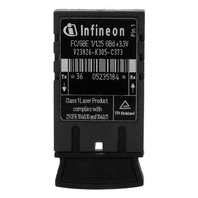
ICGOO在线商城 > 光电元件 > 光纤 - 收发器模块 > AFBR-5715APZ

 Datasheet下载
- 型号: AFBR-5715APZ
- 制造商: Avago Technologies
- 库位|库存: xxxx|xxxx
- 要求:
| 数量阶梯 | 香港交货 | 国内含税 |
| +xxxx | $xxxx | ¥xxxx |
查看当月历史价格
查看今年历史价格
AFBR-5715APZ产品简介:
ICGOO电子元器件商城为您提供AFBR-5715APZ由Avago Technologies设计生产,在icgoo商城现货销售,并且可以通过原厂、代理商等渠道进行代购。 AFBR-5715APZ价格参考。Avago TechnologiesAFBR-5715APZ封装/规格:光纤 - 收发器模块, Fiber Optic Transceiver Module Ethernet 1.25Gbps 850nm 3.3V LC Duplex Pluggable, SFP。您可以下载AFBR-5715APZ参考资料、Datasheet数据手册功能说明书,资料中有AFBR-5715APZ 详细功能的应用电路图电压和使用方法及教程。
AFBR-5715APZ是由Foxconn Optical Interconnect Technologies, Inc.生产的一款光纤收发器模块,属于高速光通信器件。该模块基于百兆以太网标准(100BASE-FX),采用SFP(小型可插拔)封装,支持单模光纤传输,典型传输距离可达10公里或更远,具备良好的信号稳定性和抗电磁干扰能力。

AFBR-5715APZ主要应用于需要高可靠性和长距离数据传输的工业与通信场景。常见用途包括:工业自动化控制系统中的远程设备互联,用于PLC、HMI和工控机之间的稳定通信;智能交通系统(如高速公路监控、信号灯控制网络)中的光纤骨干网络连接;以及电力、轨道交通等对环境适应性要求较高的领域,实现变电站、调度中心等关键节点的数据传输。

此外,该模块也适用于企业级网络扩展,例如在校园网、大型办公楼或数据中心之间构建长距离光纤链路,提升网络覆盖范围和稳定性。其宽温工作设计(-40°C至+85°C)使其能够在恶劣环境下可靠运行,满足工业级应用需求。

综上,AFBR-5715APZ凭借其长距离传输能力、高可靠性及工业级性能,广泛应用于工业控制、智能交通、能源电力及企业网络等对通信质量要求较高的场景。
| 参数 | 数值 |
| 产品目录 | |
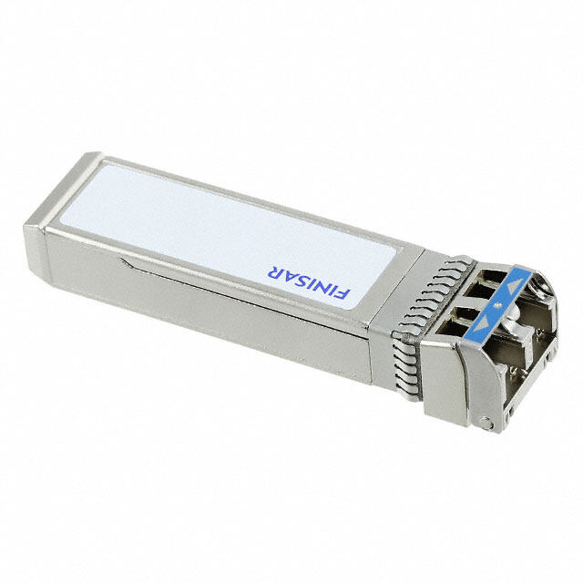
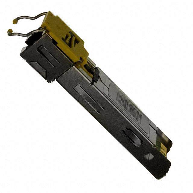
| 描述 | TXRX OPTICAL SFP DMI IND BAIL光纤发射器、接收器、收发器 Transceiver |
| 产品分类 | 光纤 - 收发器光纤 |
| 品牌 | Avago Technologies US Inc. |
| 产品手册 | http://www.avagotech.com/pages/en/optical_transceivers/ethernet/gigabit_ethernet/afbr-5715apz/ |
| 产品图片 |
|
| rohs | 符合RoHS无铅 / 符合限制有害物质指令(RoHS)规范要求 |
| 产品系列 | 光纤发射器、接收器、收发器,Avago Technologies AFBR-5715APZ- |
| mouser_ship_limit | 该产品可能需要其他文件才能进口到中国。 |
| 数据手册 | http://www.avagotech.com/docs/AV02-3012EN |
| 产品型号 | AFBR-5715APZ |
| 产品 | Transceivers |
| 产品种类 | 光纤发射器、接收器、收发器 |
| 其它名称 | 516-2343 |
| 商标 | Avago Technologies |
| 安装类型 | 可插入式,SFP |
| 封装/箱体 | SFP-20 |
| 工作电源电压 | 3.3 V |
| 工厂包装数量 | 10 |
| 应用 | 以太网 |
| 数据速率 | 1.25Gbps |
| 最大工作温度 | + 85 C |
| 最小工作温度 | - 40 C |
| 标准包装 | 10 |
| 波长 | 850nm |
| 电压-电源 | 3.135 V ~ 3.465 V |
| 纤维类型 | Multimode |
| 连接器类型 | LC 双工 |


- 商务部:美国ITC正式对集成电路等产品启动337调查
- 曝三星4nm工艺存在良率问题 高通将骁龙8 Gen1或转产台积电
- 太阳诱电将投资9.5亿元在常州建新厂生产MLCC 预计2023年完工
- 英特尔发布欧洲新工厂建设计划 深化IDM 2.0 战略
- 台积电先进制程称霸业界 有大客户加持明年业绩稳了
- 达到5530亿美元!SIA预计今年全球半导体销售额将创下新高
- 英特尔拟将自动驾驶子公司Mobileye上市 估值或超500亿美元
- 三星加码芯片和SET,合并消费电子和移动部门,撤换高东真等 CEO
- 三星电子宣布重大人事变动 还合并消费电子和移动部门
- 海关总署:前11个月进口集成电路产品价值2.52万亿元 增长14.8%


PDF Datasheet 数据手册内容提取
AFBR-5710Z and AFBR-5715Z Families of Multi-Mode Small Form Factor Pluggable (SFP) Optical Transceivers with Optional DMI for Gigabit Ethernet (1.25 GBd) Data Sheet Description Features The AFBR-571xZ family of SFP optical transceivers offers • ROHS-6 Compliant the customer a wide range of design options, includ- • Compliant to IEEE 802.3 Gigabit Ethernet (1.25GBd) ing optional DMI features (further described later), two 1000BaseSX temperature ranges (extended or industrial), and choice • Optional Digital Diagnostic Monitoring available of standard or bail delatch. The AFBR-5715Z family - AFBR-5710Z family: without DMI targets those applications requiring DMI features. The - AFBR-5715Z family: with DMI AFBR-5710Z family is a streamlined product designed for • Per SFF-8472, diagnostic features on AFBR-5715Z those applications where DMI features are not needed. family enable Diagnostic Monitoring Interface for Throughout this document, AFBR-571xZ will be used to optical transceivers with real-time monitoring of: refer collectively to the product family encompassing this - Transmitted optical power entire range of product options. - Received optical power Part Number Options - Laser bias current - Temperature The AFBR-571xZ SFP family includes the following prod- - Supply voltage ucts: • Transceiver specifications according to SFP Multi- Source Agreement (SFF-8074i) and SFF-8472, Revision Part Number DMI Temperature Latch 9.3 AFBR-5710LZ No Extended Standard • Manufactured in an ISO 9001 compliant facility AFBR-5710PZ No Extended Bail • Hot-pluggable AFBR-5710ALZ No Industrial Standard • Temperature options AFBR-5710APZ No Industrial Bail - (Extended) -10°C to +85°C AFBR-5715LZ Yes Extended Standard - (Industrial) -40°C to +85°C AFBR-5715PZ Yes Extended Bail • +3.3 V DC power supply AFBR-5715ALZ Yes Industrial Standard • Industry leading EMI performance for high port den- sity AFBR-5715APZ Yes Industrial Bail • 850 nm Vertical Cavity Surface Emitting Laser (VCSEL) * Extended Temperature Range is -10 to 85 °C • Eye safety certified Industrial Temperature Range is -40 to 85 ° C • LC-Duplex fiber connector compliant Related Products Applications • AFBR-5705Z family: Dual-Rate 1.25 GBd Ethernet • Ethernet Switch (1000BASE-SX) & 1.0625 GBd Fiber Channel SFP with • Enterprise Router DMI • Broadband aggregation and wireless infrastructure • ABCU-5710RZ family : 1.25 GBd Ethernet (1000BASE-T) SFP for Cat5 cable • Metro Ethernet multi-service access & provisioning platforms • AFCT-5705Z family: 1.25 GBd Ethernet (1000BASE-LX) & 1.0265 GBd Fiber-Channel SFP with DMI Patent - www.avagotech.com/patents
OPTICAL INTERFACE ELECTRICAL INTERFACE RECEIVER RD+ (RECEIVE DATA) AMPLIFICATION LIGHT FROM FIBER PHOTO-DETECTOR & QUANTIZATION RDÐ (RECEIVE DATA) Rx LOSS OF SIGNAL MOD-DEF2 (SDA) CONTROLLER & MEMORY MOD-DEF1 (SCL) MOD-DEF0 TRANSMITTER TX_DISABLE LASER DRIVER & TD+ (TRANSMIT DATA) LIGHT TO FIBER VCSEL SAFETY TDÐ (TRANSMIT DATA) CIRCUITRY TX_FAULT Figure 1. SFP Block Diagram Overview 3 2 1 3 2 1 ENGAGEMENT The AFBR-571xZ family of optical transceivers are com- 20 VEET SEQUENCE 1 VEET pliant with the specifications set forth in the IEEE802.3 19 TD– 2 TX FAULT (1000BASE-SX) and the Small Form-Factor Pluggable (SFP) Multi-Source Agreement (MSA). This family of transceivers 18 TD+ 3 TX DISABLE is qualified in accordance with Telcordia GR-468-CORE. Its primary application is servicing Gigabit Ethernet links 17 VEET 4 MOD-DEF(2) between optical networking equipment. 16 VCCT 5 MOD-DEF(1) The AFBR-571xZ offers maxim um flexibility to designers, 15 VCCR 6 MOD-DEF(0) manufacturers, and operators of Gigabit Ethernet net- working equipment. A pluggable architec ture allows the 14 VEER 7 RATE SELECT module to be installed into MSA standard SFP ports at 13 RD+ 8 LOS any time – even with the host equipment operating and online. This facilitates the rapid configuration of equip- 12 RD– 9 VEER ment to precisely the user’s needs – reducing inventory 11 VEER 10 VEER costs and network downtime. Compared with traditional transceivers, the size of the Small Form Factor package TOP OF BOARD BOTTOM OF BOARD enables higher port densities. (AS VIEWED THROUGH TOP OF BOARD) Module Diagrams Figure 2. Pin description of the SFP electrical interface. Figure 1 illustrates the major functional components of the AFBR-571xZ. The external configuration of the module is depicted in Figure 7. Figure 8 depicts the panel and host board footprints. 2
Installation Transmit Fault (Tx_Fault) The AFBR-571xZ can be installed in or removed from any A catastrophic laser fault will activate the transmitter signal, MSA-compliant Pluggable Small Form Factor port regard- TX_FAULT, and disable the laser. This signal is an open collec- less of whether the host equipment is operating or not. tor output (pull-up required on the host board). A low signal The module is simply inserted, electrical-interface first, indicates normal laser operation and a high signal indicates under finger-pressure. Controlled hot-plugging is ensured a fault. The TX_FAULT will be latched high when a laser fault by 3-stage pin sequencing at the electrical interface. This occurs and is cleared by toggling the TX_DISABLE input or printed circuit board card-edge connector is depicted in power cycling the transceiver. The transmitter fault condition Figure 2. can also be monitored via the 2-wire serial interface (address A2, byte 110, bit 2). As the module is inserted, first contact is made by the housing ground shield, discharging any potentially com- Eye Safety Circuit ponent-damaging static electricity. Ground pins engage next and are followed by Tx and Rx power supplies. Finally, The AFBR-571xZ provides Class 1 eye safety by design and signal lines are connected. Pin functions and sequencing has been tested for compliance with the requirements are listed in Table 2. listed in Table 1. The eye safety circuit continu ously moni- tors optical output power levels and will disable the trans- Transmitter Section mitter and assert a TX_FAULT signal upon detecting an unsafe condition. Such unsafe conditions can be created The transmitter section includes the Transmitter Optical by inputs from the host board (Vcc fluxuation, unbalanced Suba ssembly (TOSA) and laser driver circuitry. The TOSA, code) or faults within the module. containing an 850 nm VCSEL (Vertical Cavity Surface Emit- ting Laser) light source, is located at the optical interface and Receiver Section mates with the LC optical connector. The TOSA is driven by a custom IC, which converts differential logic signals into an The receiver section includes the Receiver Optical Subas- analog laser diode drive current. This Tx driver circuit regu- sembly (ROSA) and amplification/quantization circuitry. The lates the optical power at a constant level provided the data ROSA, containing a PIN photodiode and custom trans-im- pattern is DC balanced (8B10B code for example). pedance preamplifier, is located at the optical interface and mates with the LC optical connector. The ROSA is mated to Transmit Disable (Tx_Disable) a custom IC that provides post-amplification and quantiza- tion. Also included is a Loss Of Signal (LOS) detection circuit. The AFBR-571xZ accepts a TTL and CMOS compatible transmit disable control signal input (pin 3) which shuts Receiver Loss of Signal (Rx_LOS) down the transmitter optical output. A high signal imple- ments this function while a low signal allows normal The Loss Of Signal (LOS) output indicates an unusable transceiver operation. In the event of a fault (e.g. eye optical input power level. The Loss Of Signal thresholds safety circuit activated), cycling this control signal resets are set to indicate a definite optical fault has occurred the module as depicted in Figure 6. An internal pull-up (e.g., disconnected or broken fiber connection to receiver, resistor disables the transceiver transmitter until the host failed transmitter, etc.). pulls the input low. Host systems should allow a 10ms The post-amplification IC includes transition detection interval between successive assertions of this control circuitry which monitors the ac level of incoming optical signal. Tx_Disable can also be asserted via the 2-wire serial signals and provides a TTL/CMOS compatible status signal interface (address A2h, byte 110, bit 6) and monitored to the host (pin 8). An adequate optical input results in a (address A2h, byte 110, bit 7). low Rx_LOS output while a high Rx_LOS output indicates The contents of A2h, byte 110, bit 6 are logic OR’d with an unusable optical input. The Rx_LOS thresholds are fac- hardware Tx_Disable (pin 3) to control transmitter opera- tory-set so that a high output indicates a definite optical tion. fault has occurred. For the AFBR-5715Z family, Rx_LOS can also be monitored via the 2-wire serial interface (address A2h, byte 110, bit 1). 3
Functional I/O Digital Diagnostic Interface and Serial Identification (EEPROM) The AFBR-571xZ accepts industry standard differential signals such as LVPECL and CML within the scope of the The entire AFBR-571xZ family complies with the SFF- SFP MSA. To simplify board requirements, transmitter bias 8074i SFP specification. The AFBR-5715Z family further resistors and ac coupling capacitors are incorporated, per complies with SFF-8472, the SFP specification for Digital SFF-8074i, and hence are not required on the host board. Diagnostic Monitoring Interface. Both specifications can The module is AC-coupled and internally terminated. be found at http://www.sffcommittee.org. Figure 3 illustrates a recommended interface circuit to The AFBR-571xZ features an EEPROM for Serial ID, which link the AFBR-571xZ to the supporting Physical Layer contains the product data stored for retrieval by host integrated circuits. equipment. This data is accessed via the 2-wire serial EEPROM protocol of the ATMEL AT24C01A or similar, in Timing diagrams for the MSA compliant control signals compliance with the industry standard SFP Multi-Source implemented in this module are depicted in Figure 6. Agreement. The base EEPROM memory, bytes 0-255 at The AFBR-571xZ interfaces with the host circuit board memory address 0xA0, is organized in compliance with through twenty I/O pins (SFP electrical connector) SFF-8074i. Contents of this serial ID memory are shown identified by function in Table 2. The AFBR-571xZ high in Table 10. speed transmit and receive interfaces require SFP MSA The I2C accessible memory page address 0xB0 is used compliant signal lines on the host board. The Tx_Disable, internally by SFP for the test and diagnostic purposes Tx_Fault, and Rx_LOS lines require TTL lines on the host and it is reserved. board (per SFF-8074i) if used. If an application chooses not to take advantage of the functionality of these pins, care must be taken to ground Tx_Disable (for normal operation). 1 µH VCCT,R HOUSING 10 µF 0.1 µF 1 µH GROUND VCCT AVAGO *RES AFBR-571xZ 0.1 µF *RES TX_DISABLE GP04 TX_FAULT TX_FAULT VREFR 50 Ω TD+ SO1+ C R LASER DRIVER TX[0:9] SO1– 50 Ω C & EYE SAFETY TD– CIRCUITRY TBC SYNC VEET EWRAP LOOP AVAGO VCCR MAC HDMP-1687 10 0.1 ASIC RX[0:9] µF µF SYN1 SI1+ 50 Ω RD+ RX_RRABTCE RRCCM1(00:1) SI1– R 50 Ω CC RD– AMPLIF&ICATION RFCT QUANTIZATION RX_LOS VCCT,R REF_RATE *RES *RES *RES *RES RX_LOS GPIO(X) GPIO(X) MOD_DEF2 GP14 MOD_DEF1 EEPROM REFCLK MOD_DEF0 125 MHz VEER NOTE: * 4.7 k Ω < RES < 10 kΩ Figure 3. Typical application configuration. 4
As an enhancement to the conventional SFP interface component compliance issues. Received optical power is defined in SFF-8074i, the AFBR-5715Z family is compliant also available to assess compliance of a cable plant and to SFF-8472 (digital diagnostic interface for optical trans- remote transmitter. When operating out of requirements, ceivers). This new digital diagnostic information is stored the link cannot guarantee error free transmission. in bytes 0-255 at memory address 0xA2.Using the 2-wire Fault Isolation serial interface defined in the MSA, the AFBR-5715Z provides real time temperature, supply voltage, laser The fault isolation feature allows a host to quickly pin- bias current, laser average output power and received point the location of a link failure, minimizing downtime. input power. These parameters are internally calibrated, For optical links, the ability to identify a fault at a local per the MSA. device, remote device or cable plant is crucial to speeding The digital diagnostic interface also adds the ability to service of an installation. AFBR-5715Z real-time monitors disable the transmitter (TX_DISABLE), monitor for Trans- of Tx_Bias, Tx_Power, Vcc, Temperature and Rx_Power mitter Faults (TX_FAULT), and monitor for Receiver Loss can be used to assess local transceiver current operating of Signal (RX_LOS). conditions. In addition, status flags Tx_Disable and Rx Loss of Signal (LOS) are mirrored in memory and available via The new diagnostic information provides the oppor- the two-wire serial interface. tunity for Predictive Failure Identification, Compliance Prediction, Fault Isolation and Component Monitoring. Component Monitoring Predictive Failure Identification Component evaluation is a more casual use of the AFBR- 5715Z real-time monitors of Tx_Bias, Tx_Power, Vcc, Tem- The predictive failure feature allows a host to identify perature and Rx_Power. Potential uses are as debugging potential link problems before system performance is aids for system installation and design, and transceiver impacted. Prior identification of link problems enables parametric evaluation for factory or field qualification. a host to service an application via “fail over” to a redun- For example, temperature per module can be observed in dant link or replace a suspect device, maintaining system high density applications to facilitate thermal evaluation uptime in the process. For applications where ultra-high of blades, PCI cards and systems. system uptime is required, a digital SFP provides a means to monitor two real-time laser metrics associated with ob- Required Host Board Components serving laser degradation and predicting failure: average The MSA power supply noise rejection filter is required on laser bias current (Tx_Bias) and average laser optical power the host PCB to meet data sheet performance. The MSA (Tx_Power). filter incorporates an inductor which should be rated 400 Compliance Prediction mADC and 1 Ω series resistance or better. It should not be replaced with a ferrite. The required filter is illustrated Compliance prediction is the ability to determine if an in Figure 4. optical transceiver is operating within its operating and environmental requirements. AFBR-5715Z devices provide The MSA also specifies that 4.7 K to 10 KΩ pull-up resis- real-time access to transceiver internal supply voltage tors for TX_FAULT, LOS, and MOD_DEF0,1,2 are required and temperature, allowing a host to identify potential on the host PCB. 1 µH V T CC 0.1 µF 1 µH V R 3.3 V CC 0.1 µF 10 µF 0.1 µF 10 µF SFP MODULE HOST BOARD Figure 4. MSA required power supply filter. 5
Fiber Compatibility Electromagnetic Interference (EMI) The AFBR-571xZ transciever is capable of transmission Equipment using the AFBR-571xZ family of transceivers at 2 to 550 meters with 50/125 µm fiber, and at 2 to 275 is typically required to meet the requirem ents of the meters with 62.5 125 µm fiber, for 1.25 GBd Ethernet. It FCC in the United States, CENELEC EN55022 (CISPR 22) is capable of transmission up to 500m with 50/125 µm in Europe, and VCCI in Japan. fiber and up to 300m with 62.5/125 µm fiber, for 1.0625 The metal housing and shielded design of the AFBR- GBd Fiber Channel. 571xZ minimize the EMI challenge facing the host equip- Application Support ment designer. To assist in the transceiver evaluation process, Agilent EMI Immunity offers a 1.25 Gbd Gigabit Ethernet evaluation board Equipment hosting AFBR-571xZ modules will be sub- which facilitates testing of the AFBR-571xZ. It can be jected to radio-frequency electromagnetic fields in some obtained through the Agilent Field Organization by ref- environments. The transceiver has excellent immunity to erencing Agilent part number HFBR-0571. such fields due to its shielded design. A Reference Design including the AFBR-571xZ and the Flammability HDMP-1687 GigaBit Quad SerDes is available. It may be obtained through the Agilent Field Sales organization. The AFBR-571xZ transceiver is made of metal and high strength, heat resistant, chemically resistant, and UL Regulatory Compliance 94V-0 flame retardant plastic. See Table 1 for transceiver Regulatory Compliance. Certi- Customer Manufacturing Processes fication level is dependent on the overall configuration of the host equipment. The transceiver performance is This module is pluggable and is not designed for aqueous offered as a figure of merit to assist the designer. wash, IR reflow, or wave soldering processes. Electrostatic Discharge (ESD) The AFBR-571xZ exceeds typical industry standards and is compatible with ESD levels found in typical manufactur- ing and operating environments as described in Table 1. There are two design cases in which immunity to ESD damage is important. The first case is during handling of the transceiver prior to insertion into the transceiver port. To protect the trans- ceiver, it’s important to use normal ESD handling precau- tions. These precautions include using grounded wrist straps, work benches, and floor mats in ESD controlled areas. The ESD sensitivity of the AFBR-571xZ is compat- ible with typical industry production environments. The second case to consider is static discharges to the exterior of the host equipment chassis after installation. To the extent that the optical interface is exposed to the outside of the host equipment chassis, it may be subject to system-level ESD requirements. 6
Table 1. Regulatory Compliance Feature Test Method Performance Electrostatic Discharge JEDEC/EIAJESD22-A114-A Class 2 (> +2000 Volts) (ESD)to the Electrical Pins Electrostatic Discharge Variation of IEC 6100-4-2 Typically withstands at least 25 kV without (ESD) to the Duplex LC damage when the duplex LC connector receptacle Reseptacle is contacted by a Human Body Model probe Electromagnetic FCC Class B CENELEC EN55022 Applications with high SFP port counts are Interference(EMI) Class B (CISPR 22A) VCCI Class 1 expected to be compliant; however, margins are dependent on customer board and chassis design. Immunity Variation of IEC 61000-4-3 Typically shows a negligible effect from a 10 V/m field swept from 80 to 1000 MHz applied to the transceiver without a chassis enclosure. Eye Safety US FDA CDRH AEL Class 1 CDRH certification #9720151-57 EN(IEC)60825-1,2, EN60950 Class 1 TUV file RR72102090.01 Component Recognition Underwriters Laboratories and Canadian UL File #E173874 Standards Association Joint Component Recognition for Information Technology Equipment Including Electrical Business Equipment ROHS Compliance Less than 1000ppm of: cadmium, lead, mercury, hexavalent chromium, polybrominated biphenyls, and polybrominated biphenyl ethers. Caution There are no user serviceable parts nor any maintenance required for the AFBR-571xZ. All adjustments are made at the factory before shipment to our customers. Tampering with, modifying, misusing or improp erly handling the AFBR-571xZ will void the product warranty. It may also result in improper operation of the AFBR-571xZ circuitry, and possible overstress of the laser source. Device deg- radation or product failure may result. Connection of the AFBR-571xZ to a non-Gigabit Ethernet compliant or non- Fiber Channel compliant optical source, operating above the recommended absolute maximum conditions or operating the AFBR-571xZ in a manner inconsistent with its design and function may result in hazardous radiation exposure and may be considered an act of modifying or manufacturing a laser product. The person(s) performing such an act is required by law to re-certify and re-identify the laser product under the provisions of U.S. 21 CFR (Subchapter J). 7
Table 2. Pin Description Engagement Order Pin Name Function/Description (insertion) Notes 1 VeeT Transmitter Ground 1 2 TX Fault Transmitter Fault Indication 3 1 3 TX Disable Transmitter Disable - Module disables on high or open 3 2 4 MOD-DEF2 Module Definition 2 - Two wire serial ID interface 3 3 5 MOD-DEF1 Module Definition 1 - Two wire serial ID interface 3 3 6 MOD-DEF0 Module Definition 0 - Grounded in module 3 3 7 Rate Selection Not Connected 3 8 LOS Loss of Signal 3 4 9 VeeR Receiver Ground 1 10 VeeR Receiver Ground 1 11 VeeR Receiver Ground 1 12 RD- Inverse Received Data Out 3 5 13 RD+ Received Data Out 3 5 14 VeeR Reciver Ground 1 15 VccR Receiver Power -3.3 V ±5% 2 6 16 VccT Transmitter Power -3.3 V ±5% 2 6 17 VeeT Transmitter Ground 1 18 TD+ Transmitter Data In 3 7 19 TD- Inverse Transmitter Data In 3 7 20 VeeT Transmitter Ground 1 Notes: 1. TX Fault is an open collector/drain output which should be pulled up externally with a 4.7KΩ – 10 KΩ resistor on the host board to a supply <VccT+0.3 V or VccR+0.3 V. When high, this output indicates a laser fault of some kind. Low indicates normal operation. In the low state, the output will be pulled to < 0.8 V. 2. TX disable input is used to shut down the laser output per the state table below. It is pulled up within the module with a 4.7-10 KΩ resistor. Low (0 – 0.8 V): Transmitter on Between (0.8 V and 2.0 V): Undefined High (2.0 – 3.465 V): Transmitter Disabled Open: Transmitter Disabled 3. Mod-Def 0,1,2. These are the module definition pins. They should be pulled up with a 4.7-10 KΩ resistor on the host board to a supply less than VccT +0.3 V or VccR+0.3 V. Mod-Def 0 is grounded by the module to indicate that the module is present Mod-Def 1 is clock line of two wire serial interface for optional serial ID Mod-Def 2 is data line of two wire serial interface for optional serial ID 4. LOS (Loss of Signal) is an open collector/drain output which should be pulled up externally with a 4.7 K – 10 KΩ resistor on the host board to a supply < VccT,R+0.3 V. When high, this output indicates the received optical power is below the worst case receiver sensitivity (as defined by the standard in use). Low indicates normal operatio0n. In the low state, the output will be pulled to < 0.8 V. 5. RD-/+: These are the differential receiver outputs. They are AC coupled 100 Ω differential lines which should be terminated with 100 Ω differential at the user SERDES. The AC coupling is done inside the module and is thus not required on the host board. The voltage swing on these lines must be between 370 and 2000 mV differential (185 – 1000 mV single ended) according to the MSA. Typically it will be 1500mv differential. 6. VccR and VccT are the receiver and transmitter power supplies. They are defined as 3.135 – 3.465 V at the SFP connector pin. The in-rush current will typically be no more than 30 mA above steady state supply current after 500 nanoseconds. 7. TD-/+: These are the differential transmitter inputs. They are AC coupled differential lines with 100 Ω differential termination inside the module. The AC coupling is done inside the module and is thus not required on the host board. The inputs will accept differential swings of 500 – 2400 mV (250 – 1200 mV single ended). However, the applicable recommended differential voltage swing is found in Table 5. 8
Table 3. Absolute Maximum Ratings Parameter Symbol Minimum Maximum Unit Notes Ambient Storage Temperature Ts -40 +100 °C 1, 2 (Non-operating) Case Temperature TC -40 +85 °C 1, 2 Relative Humidity RH 5 95 % 1 Supply Voltage VCCT,R -0.5 3.8 V 1, 2, 3 Low Speed Input Voltage VIN -0.5 VCC+0.5 V 1 Notes: 1. Absolute Maximum Ratings are those values beyond which damage to the device may occur if these limits are exceeded. See Reliability Data Sheet for specific reliability performance. 2. Between Absolute Maximum Ratings and the Recommended Operating Conditions functional performance is not intended, device reliability is not implied, and damage to the device may occur. 3. The module supply voltages, VCCT and VCCR, must not differ by more than 0.5V or damage to the device may occur. Table 4. Recommended Operating Conditions Parameter Symbol Minimum Typical Maximum Unit Notes Case Temperature AFBR-571xLZ/PZ TC -10 25 85 °C 1, 2 AFBR-571xALZ/APZ TC -40 25 85 °C 1, 2 Supply Voltage VCC 3.135 3.3 3.465 V 1 Notes: 1. Recommended Operating Conditions are those within which functional performance within data sheet characteristics is intended. 2. Refer to the Reliability Data Sheet for specific reliability performance predictions. Table 5. Transceiver Electrical Characteristics Parameter Symbol Minimum Typical Maximum Unit Notes Module Supply Current ICC 160 220 mA Power Dissipation PDISS 530 765 mW Power Supply Noise PSNR 100 mVPP 1 Rejection(peak-peak) Data input: VI 500 2400 mVPP 2 Transmitter Differential Input Voltage (TD +/-) Data Output: VO 370 1500 2000 mVPP 3 Receiver Differential Output Voltage (RD +/-) Receive Data Rise & Fall Times T 220 ps rf Low Speed Outputs: VOH 2.0 VCCT,R+0.3 V 4 Transmit Fault (TX_FAULT) Loss of Signal (LOS), MOD_DEF2 VOL 0 0.8 V Low Speed Inputs: VIH 2.0 VCC V 5 Transmitter Disable(TX_DISABLE), MOD_DEF 1, MOD_DEF 2 VIL 0 0.8 V Notes: 1. Measured at the input of the required MSA Filter on host board. 2. Internally AC coupled and terminated to 100 Ω differential load. 3. Internally AC coupled, but requires a 100 Ω differential termination at or internal to Serializer/Deserializer. 4. Pulled up externally with a 4.7-10 KΩ resistor on the host board to VCCT,R. 5. Mod_Def1 and Mod_Def2 must be pulled up externally with a 4.7-10 KΩ resistor on the host board to VCCT,R. 9
Table 6. Transmitter Optical Characteristics Parameter Symbol Minimum Typical Maximum Unit Notes Output Optical Power (Average) POUT -9.5 -6.5 -3 dBm 1 Optical Extinction Ratio ER 9 12 dB Center Wavelength lC 830 850 860 nm Spectral Width - rms s 0.85 nm Optical Rise/Fall Time Trise/fall 150 260 ps Relative Intensity Noise RIN -117 dB/Hz Total Jitter (TP1 to TP2 Contribution TJ 227 ps 0.284 UI Pout TX_DISABLE Assorted POFF -35 dBm Notes: 1. 50/125 µm fiber with NA = 0.2, 62.5/125 µm fiber with NA = 0.275. NORMALIZED TIME (UNIT INTERVAL) 0 0.22 0.375 0.625 0.78 1.0 130 1.30 100 1.00 %) PLITUDE ( 80 0.80 MPLITUDE M A A 50 0.50 D ALIZED MALIZE ORM 20 0.20 NOR N 0 0 –20 –0.20 0 22 37.5 62.5 78 100 NORMALIZED TIME (% OF UNIT INTERVAL) Figure 5a. Gigabit Ethernet transmitter eye mask diagram Figure 5b. Typical AFBR-571xZ eye mask diagram Table 7. Receiver Optical Characteristics Parameter Symbol Minimum Typical Maximum Unit Notes Optical Input Power PR -17 0 dBm Receiver Sensitivity PRMIN -21 -17 dBm (Optical Input Power) Stressed Receiver Sensitivity -12.5 dBm 62.5/125 mm fiber -13.5 dBm 50/125 mm fiber Total Jitter TJ 266 ps (TP3 to TP4 Contribution 1.25GBd) 0.332 UI Return Loss -12 dB LOS De-Asserted PD - -17 dBm LOS Asserted PA -30 dBm LOS Hysterisis PD-PA 3 dB 10
Table 10. Transceiver SOFT DIAGNOSTIC Timing Characteristics Parameter Symbol Minimum Maximum Unit Notes Hardware TX_DISABLE Assert Time t_off 10 µs Note 1 Hardware TX_DISABLE Negate Time t_on 1 ms Note 2 Time to initialize, including reset of TX_FAULT t_init 300 ms Note 3 Hardware TX_FAULT Assert Time t_fault 100 µs Note 4 Hardware TX_DISABLE to Reset t_reset 10 µs Note 5 Hardware RX_LOS Assert Time t_loss_on 100 µs Note 6 Hardware RX_LOS De-Assert Time t_loss_off 100 µs Note 7 Software TX_DISABLE Assert Time t_off_soft 100 ms Note 8 Software TX_DISABLE Negate Time t_on_soft 100 ms Note 9 Software Tx_FAULT Assert Time t_fault_soft 100 ms Note 10 Software Rx_LOS Assert Time t_loss_on_soft 100 ms Note 11 Software Rx_LOS Deassert Time t_loss_off_soft 100 ms Note 12 Analog parameter data ready t_data 1000 ms Note 13 Serial bus hardware ready t_serial 300 ms Note 14 Write Cycle Time t_write 10 ms Note 15 Serial ID Clock Rate f_serial_clock 400 kHz Notes: 1. Time from rising edge of TX_DISABLE to when the optical output falls below 10% of nominal. 2. Time from falling edge of TX_DISABLE to when the modulated optical output rises above 90% of nominal. 3. Time from power on or falling edge of Tx_Disable to when the modulated optical output rises above 90% of nominal. 4. From power on or negation of TX_FAULT using TX_DISABLE. 5. Time TX_DISABLE must be held high to reset the laser fault shutdown circuitry. 6. Time from loss of optical signal to Rx_LOS Assertion. 7. Time from valid optical signal to Rx_LOS De-Assertion. 8. Time from two-wire interface assertion of TX_DISABLE (A2h, byte 110, bit 6) to when the optical output falls below 10% of nominal. Measured from falling clock edge after stop bit of write transaction. 9. Time from two-wire interface de-assertion of TX_DISABLE (A2h, byte 110, bit 6) to when the modulated optical output rises above 90% of nominal. 10. Time from fault to two-wire interface TX_FAULT (A2h, byte 110, bit 2) asserted. 11. Time for two-wire interface assertion of Rx_LOS (A2h, byte 110, bit 1) from loss of optical signal. 12. Time for two-wire interface de-assertion of Rx_LOS (A2h, byte 110, bit 1) from presence of valid optical signal. 13. From power on to data ready bit asserted (A2h, byte 110, bit 0). Data ready indicates analog monitoring circuitry is functional. 14. Time from power on until module is ready for data transmission over the serial bus (reads or writes over A0h and A2h). 15. Time from stop bit to completion of a 1-8 byte write command. 11
Table 9. Transceiver Digital Diagnostic Monitor (Real Time Sense) Characteristics Parameter Symbol Min. Units Notes Transceiver Internal Temperature TINT ±3.0 °C Temperature is measured internal to the transceiver. Accuracy Valid from = -40°C to 85°C case temperature. Transceiver Internal Supply VINT ±0.1 V Supply voltage is measured internal to the transceiver Voltage Accuracy and can, with less accuracy, be correlated to voltage at the SFP Vcc pin. Valid over 3.3 V ± 5%. Transmitter Laser DC Bias Current IINT ±10 % IINT is better than ±10% of the nominal value. Accuracy Transmitted Average Optical PT ±3.0 dB Coupled into 50/125 µm multi-mode fiber. Output Power Accuracy Valid from 100 µW to 500 µW, avg. Received Average Optical Input PR ±3.0 dB Coupled from 50/125 µm multi-mode fiber. Power Accuracy Valid from 31 µW to 500 µW, avg. VCC > 3.15 V VCC > 3.15 V TX_FAULT TX_FAULT TX_DISABLE TX_DISABLE TRANSMITTED SIGNAL TRANSMITTED SIGNAL t_init t_init t-init: TX DISABLE NEGATED t-init: TX DISABLE ASSERTED VCC > 3.15 V TX_FAULT TX_FAULT TX_DISABLE TX_DISABLE TRANSMITTED SIGNAL TRANSMITTED SIGNAL t_off t_on t_init INSERTION t-init: TX DISABLE NEGATED, MODULE HOT PLUGGED t-off & t-on: TX DISABLE ASSERTED THEN NEGATED OCCURANCE OF FAULT OCCURANCE OF FAULT TX_FAULT TX_FAULT TX_DISABLE TX_DISABLE TRANSMITTED SIGNAL TRANSMITTED SIGNAL t_fault * SFP SHALL CLEAR TX_FAULT IN t_reset t_init* t_init IF THE FAILURE IS TRANSIENT t-fault: TX FAULT ASSERTED, TX SIGNAL NOT RECOVERED t-reset: TX DISABLE ASSERTED THEN NEGATED, TX SIGNAL RECOVERED OCCURANCE OF FAULT OPTICAL SIGNAL TX_FAULT OCCURANCE OF LOSS TX_DISABLE TRANSMITTED SIGNAL LOS t_fault2 t_reset t_loss_on t_loss_off * SFP SHALL CLEAR TŒ_FAULT IN t_init* t_init IF THE FAILURE IS TRANSIENT t-fault2: TX DISABLE ASSERTED THEN NEGATED, t-loss-on & t-loss-off TX SIGNAL NOT RECOVERED NOTE: t_fault2 timing is typically 1.7 to 2 ms. Figure 6. Transceiver timing diagrams (Module installed except where noted). 12
Table 10. EEPROM Serial ID Memory Contents, Page A0h Byte # Data Byte # Data Decimal Hex Notes Decimal Hex Notes 0 03 SFP physical device 37 00 Vendor OUI (Note 4) 1 04 SFP function defined by serial ID only 38 17 Vendor OUI (Note 4) 2 07 LC optical connector 39 6A Vendor OUI (Note 4) 3 00 40 41 "A" - Vendor Part Number ASCII character 4 00 41 46 "F" - Vendor Part Number ASCII character 5 00 42 42 "B" - Vendor Part Number ASCII character 6 01 1000BaseSX 43 52 "R" - Vendor Part Number ASCII character 7 00 44 2D "-" - Vendor Part Number ASCII character 8 00 45 35 "5" - Vendor Part Number ASCII character 9 00 46 37 "7" - Vendor Part Number ASCII character 10 00 47 31 "1" - Vendor Part Number ASCII character 11 01 Compatible with 8B/10B encoded data 48 Note 5 12 0C 1200Mbps nominal bit rate (1.25Gbps) 49 Note 5 13 00 50 Note 5 14 00 51 Note 5 15 00 52 20 “ “ - Vendor Part Number ASCII character 16 37 550m of 50/125mm fiber @ 1.25Gbps 53 20 " " - Vendor Part Number ASCII character (Note 2) 17 1B 275m of 62.5/125mm fiber @ 1.25Gbps 54 20 " " - Vendor Part Number ASCII character (Note 3) 18 00 55 20 " " - Vendor Part Number ASCII character 19 00 56 20 " " - Vendor Revision Number ASCII character 20 41 'A' - Vendor Name ASCII character 57 20 " " - Vendor Revision Number ASCII character 21 56 "V" - Vendor Name ASCII character 58 20 “ “ - Vendor Revision Number ASCII character 22 41 "A" - Vendor Name ASCII character 59 20 “ “ - Vendor Revision Number ASCII character 23 47 "G"- - Vendor Name ASCII character 60 03 Hex Byte of Laser Wavelength (Note 6) 24 4F "O" - Vendor Name ASCII character 61 52 Hex Byte of Laser Wavelength (Note 6) 25 20 " " - Vendor Name ASCII character 62 00 26 20 “ “ - Vendor Name ASCII character 63 Checksum for bytes 0-62 (Note 7) 27 20 “ “ - Vendor Name ASCII character 64 00 28 20 “ “ - Vendor Name ASCII character 65 1A Hardware SFP TX_DISABLE, TX_FAULT, & RX_LOS 29 20 “ “ - Vendor Name ASCIIcharacter 66 00 30 20 “ “ - Vendor Name ASCIIcharacter 67 00 31 20 “ “ - Vendor Name ASCIIcharacter 68-83 Vendor Serial Number, ASCII (Note 8) 32 20 “ “ - Vendor Name ASCIIcharacter 84-91 Vendor Date Code, ASCII (Note 9) 33 20 “ “ - Vendor Name ASCIIcharacter 92 Note 5 34 20 “ “ - Vendor Name ASCIIcharacter 93 Note 5 35 20 “ “ - Vendor Name ASCIIcharacter 94 Note 5 36 00 95 Checksum for bytes 64-94 (Note 7) 96 - 255 00 Notes: 1. FC-PI speed 100 MBytes/sec is a serial bit rate of 1.0625 GBit/sec. 2. Link distance with 50/125µm cable at 1.25Gbps is 550m. 3. Link distance with 62.5/125µm cable at 1.25Gbps is 275m. 4. The IEEE Organizationally Unique Identifier (OUI) assigned to Avago Technologies is 00-17-6A (3 bytes of hex). 5. See Table 11 for part number extensions and data-fields. 6. Laser wavelength is represented in 16 unsigned bits. The hex representation of 850nm is 0352. 7. Addresses 63 and 95 are checksums calculated per SFF-8472 and SFF-8074, and stored prior to product shipment. 8. Addresses 68-83 specify the module’s ASCII serial number and will vary by unit. 9. Addresses 84-91 specify the module’s ASCII date code and will vary according to manufactured date-code. 13
Table 11. Part Number Extensions AFBR-5710ALZ AFBR-5710APZ AFBR-5710LZ AFBR-5710PZ Address Hex ASCII Address Hex ASCII Address Hex ASCII Address Hex ASCII 48 30 0 48 30 0 48 30 0 48 30 0 49 41 A 49 41 A 49 4C L 49 50 P 50 4C L 50 50 P 50 5A Z 50 5A Z 51 5A Z 51 5A Z 51 20 51 20 92 00 92 00 92 00 92 00 93 00 93 00 93 00 93 00 94 00 94 00 94 00 94 00 AFBR-5715ALZ AFBR-5715APZ AFBR-5715LZ AFBR-5715PZ Address Hex ASCII Address Hex ASCII Address Hex ASCII Address Hex ASCII 48 35 5 48 35 5 48 35 5 48 35 5 49 41 A 49 41 A 49 4C L 49 50 P 50 4C L 50 50 P 50 5A Z 50 5A Z 51 5A Z 51 5A Z 51 20 51 20 92 68 92 68 92 68 92 68 93 F0 93 F0 93 F0 93 F0 94 01 94 01 94 01 94 01 14
Table 12. EEPROM Serial ID Memory Contents - Address A2h (AFBR-5715Z family only) Byte Byte Byte #Decimal Notes #Decimal Notes #Decimal Notes 0 Temp H Alarm MSB1 26 Tx Pwr L Alarm MSB4 104 Real Time Rx PAV MSB5 1 Temp H Alarm LSB1 27 Tx Pwr L Alarm LSB4 105 Real Time Rx PAV LSB5 2 Temp L Alarm MSB1 28 Tx Pwr H Warning MSB4 106 Reserved 3 Temp L Alarm LSB1 29 Tx Pwr H Warning LSB4 107 Reserved 4 Temp H Warning MSB1 30 Tx Pwr L Warning MSB4 108 Reserved 5 Temp H Warning LSB1 31 Tx Pwr L Warning LSB4 109 Reserved 6 Temp L Warning MSB1 32 Rx Pwr H Alarm MSB5 110 Status/Control - see Table 13 7 Temp L Warning LSB1 33 Rx Pwr H Alarm LSB5 111 Reserved 8 VCC H Alarm MSB2 34 Rx Pwr L Alarm MSB5 112 Flag Bits - see Table 14 9 VCC H Alarm LSB2 35 Rx Pwr L Alarm LSB5 113 Flag Bit - see Table 14 10 VCC L Alarm MSB2 36 Rx Pwr H Warning MSB5 114 Reserved 11 VCC L Alarm LSB2 37 Rx Pwr H Warning LSB5 115 Reserved 12 VCC H Warning MSB2 38 Rx Pwr L Warning MSB5 116 Flag Bits - see Table 14 13 VCC H Warning LSB2 39 Rx Pwr L Warning LSB5 117 Flag Bits - see Table 14 14 VCC L Warning MSB2 40-55 Reserved 118 Reserved 15 VCC L Warning LSB2 56-94 External Calibration Constants6 119 Reserved 16 Tx Bias H Alarm MSB3 95 Checksum for Bytes 0-947 120-122 Reserved 17 Tx Bias H Alarm LSB3 96 Real Time Temperature MSB1 123 18 Tx Bias L Alarm MSB3 97 Real Time Temperature LSB1 124 19 Tx Bias L Alarm LSB3 98 Real Time Vcc MSB2 125 20 Tx Bias H Warning MSB3 99 Real Time Vcc LSB2 126 21 Tx Bias H Warning LSB3 100 Real Time Tx Bias MSB3 127 Reserved8 22 Tx Bias L Warning MSB3 101 Real Time Tx Bias LSB3 128-247 Customer Writable9 23 Tx Bias L Warning LSB3 102 Real Time Tx Power MSB4 248-255 Vendor Specific 24 Tx Pwr H Alarm MSB4 103 Real Time Tx Power LSB4 25 Tx Pwr H Alarm LSB4 Notes: 1. Temperature (Temp) is decoded as a 16 bit signed twos compliment integer in increments of 1/256 °C. 2. Supply voltage (VCC) is decoded as a 16 bit unsigned integer in increments of 100 µV. 3. Laser bias current (Tx Bias) is decoded as a 16 bit unsigned integer in increments of 2 µA. 4. Transmitted average optical power (Tx Pwr) is decoded as a 16 bit unsigned integer in increments of 0.1 µW. 5. Received average optical power (Rx Pwr) is decoded as a 16 bit unsigned integer in increments of 0.1 µW. 6. Bytes 55-94 are not intended from use with AFBR-5715Z, but have been set to default values per SFF-8472. 7. Bytes 95 is a checksum calculated (per SFF-8472) and stored prior to product shipment. 8. Byte 127 accepts a write but performs no action (reserved legacy byte). 9. Bytes 128-247 are write enabled (customer writable). 15
Table 13. EEPROM Serial ID Memory Contents - Address A2h, Byte 110 (AFBR-5715Z family only) Bit # Status/Control Name Description 7 Tx Disable State Digital state of SFP Tx Disable Input Pin (1 = Tx_ Disable asserted) 6 Soft Tx Disable Read/write bit for changing digital state of SFP Tx_Disable function1 5 Reserved 4 Rx Rate Select State Digital state of SFP Rate Select Input Pin (1 = full bandwidth of 155 Mbit)2 3 Reserved 2 Tx Fault State Digital state of the SFP Tx Fault Output Pin (1 = Tx Fault asserted) 1 Rx LOS State Digital state of the SFP LOS Output Pin (1 = LOS asserted) 0 Data Ready (Bar) Indicates transceiver is powered and real time sense data is ready (0 = Ready) Notes: 1. Bit 6 is logic OR’d with the SFP Tx_Disable input pin 3 ... either asserted will disable the SFP transmitter. 2. AFBR-5715Z does not respond to state changes on Rate Select Input Pin. It is internally hardwired to full bandwidth. Table 14. EEPROM Serial ID Memory Contents - Address A2h, Bytes 112, 113, 116, 117 (AFBR-5715Z family only) Byte Bit # Flag Bit Name Description 112 7 Temp High Alarm Set when transceiver nternal temperature exceeds high alarm threshold. 6 Temp Low Alarm Set when transceiver internal temperature exceeds alarm threshold. 5 VCC High Alarm Set when transceiver internal supply voltage exceeds high alarm threshold. 4 VCC Low Alarm Set when transceiver internal supply voltage exceeds low alarm threshold. 3 Tx Bias High Alarm Set when transceiver laser bias current exceeds high alarm threshold. 2 Tx Bias Low Alarm Set when transceiver laser bias current exceeds low alarm threshold. 1 Tx Power High Alarm Set when transmitted average optical power exceeds high alarm threshold. 0 Tx Power Low Alarm Set when transmitted average optical power exceeds low alarm threshold. 113 7 Rx Power High Alarm Set when received P_Avg optical power exceeds high alarm threshold. 6 Rx Power Low Alarm Set when received P_Avg optical power exceeds low alarm threshold. 0-5 Reserved 116 7 Temp High Warning Set when transceiver internal temperature exceeds high warning threshold. 6 Temp Low Warning Set when transceiver internal temperature exceeds low warning threshold. 5 VCC High Warning Set when transceiver internal supply voltage exceeds high warning threshold. 4 VCC Low Warning Set when transceiver internal supply voltage exceeds low warning threshold. 3 Tx Bias High Warning Set when transceiver laser bias current exceeds high warning threshold. 2 Tx Bias Low Warning Set when transceiver laser bias current exceeds low warning threshold. 1 Tx Power High Warning Set when transmitted average optical power exceeds high warning threshold. 0 Tx Power Low Warning Set when transmitted average optical power exceeds low warning threshold. 117 7 Rx Power High Warning Set when received P_Avg optical power exceeds high warning threshold. 9 Rx Power Low Warning Set when received P_Avg optical power exceeds low warning threshold. 0-5 Reserved 16
AVAGO AFBR-571xZ 850 nm LASER PROD 21CFR(J) CLASS 1 TCASE REFERENCE POINT COUNTRY OF ORIGIN YYWW TUV XXXXXX UK 10.4 ±0.2 47.5 ±0.2 0.409 ±0.008 1.87 ±0.008 13.7 ±0.1 13.45 ±0.1 0.539 ±0.004 11.05 0.53 ±0.004 21 LATCH COLOR 0.70UNCOMPRESSED 13.01 ±0.2 8.5 ±0.1 6.25 ±0.05 0.512 ±0.008 0.335 ±0.004 0.246 ±0.002 BOTTOM LABEL RECESS 18.1 14.8 UNCOMPRESSED TX RX 11.8 ±0.2 .465 ±.008 6.65 13.4 STANDARD DELATCH WITH PROCESS PLUG Figure 7. Module drawing 17
X Y 34.5 3x 10 7.2 7.1 10x 1.05 ± 0.01 16.25 ∅0.1 S X A S 2.5 ∅ 0.85 ± 0.05 MIN. PITCH B 1 2.5 ∅ 0.1 S X Y PCB A 1 EDGE 3.68 5.68 PIN 1 20 8.58 2x 1.7 8.48 11.08 11.93 16.2514.25 9.6 REF. 4.8 11 10 SEE DETAIL 1 11x 2.0 9x 0.95 ± 0.05 11x 2.0 ∅ 0.1 L X A S 26.8 5 2 3 3x 10 41.3 42.3 5 20x 0.5 ± 0.03 3.2 0.9 0.06 S A S B S PIN 1 20 NOTES 10.93 10.53 11.93 1. PADS AND VIAS ARE CHASSIS GROUND 9.6 2. THROUGH HOLES, PLATING OPTIONAL. 0.8 TYP. 3. HATCHED AREA DENOTES COMPONENT AND 11 TRACE KEEPOUT (EXCEPT CHASSIS GROUND). 10 4. AREA DENOTES COMPONENT KEEPOUT (TRACES ALLOWED). 4 DIMENSIONS IN MILLIMETERS 2 ± 0.05T YP. 2x 1.55 ± 0.05 0.06 L A S B S ∅ 0.1 L A S B S DETAIL 1 Figure 8. SFP host board mechanical layout 18
1.7 ± 0.9 (0.07 ± 0.04) 3.5 ± 0.3 (0.14 ± 0.01) 41.73 ± 0.5 PCB (1.64 ± 0.02) BEZEL AREA 15 MAX. FOR (0.59) PROCESS PLUG CAGE ASSEMBLY 15.25 ± 0.1 (0.60 ± 0.004) 11 REF. (0.43) 9.8 10.4 ± 0.1 MAX. (0.39) (0.41 ± 0.004) 10 REF 1.5 REF. (0.39) (0.06) TO PCB 16.25 ± 0.1 MIN. PITCH BELOW PCB (0.64 ± 0.004) 0.4 ± 0.1 (0.02 ± 0.004) MSA-SPECIFIED BEZEL BELOW PCB DIMENSIONS ARE IN MILLIMETERS (INCHES). Figure 9. Assembly drawing 19
Ordering Information Please contact your local field sales engineer or one of Avago Technologies franchised distributors for ordering infor- mation. For technical information, please visit Avago Technologies’ web-page at www.avagotech.com or contact one of Avago Technologies’ regional Technical Response Centers. For information related to SFF Committee documentation visit www.sffcommittee.org. For product information and a complete list of distributors, please go to our web site: www.avagotech.com Avago, Avago Technologies, and the A logo are trademarks of Avago Technologies in the United States and other countries. Data subject to change. Copyright © 2005-2016 Avago Technologies. All rights reserved. Obsoletes AV01-0181EN AV02-3012EN - January 7, 2016