ICGOO在线商城 > 光电元件 > 光纤 - 收发器模块 > AFCT-5805AZ

 Datasheet下载
- 型号: AFCT-5805AZ
- 制造商: Avago Technologies
- 库位|库存: xxxx|xxxx
- 要求:
| 数量阶梯 | 香港交货 | 国内含税 |
| +xxxx | $xxxx | ¥xxxx |
查看当月历史价格
查看今年历史价格
AFCT-5805AZ产品简介:
ICGOO电子元器件商城为您提供AFCT-5805AZ由Avago Technologies设计生产,在icgoo商城现货销售,并且可以通过原厂、代理商等渠道进行代购。 AFCT-5805AZ价格参考。Avago TechnologiesAFCT-5805AZ封装/规格:光纤 - 收发器模块, Fiber Optic Transceiver Module General Purpose 155Mbps 1300nm 3.3V, 5V SC Through Hole。您可以下载AFCT-5805AZ参考资料、Datasheet数据手册功能说明书,资料中有AFCT-5805AZ 详细功能的应用电路图电压和使用方法及教程。
AFCT-5805AZ 是由富士康旗下子公司 Foxconn Optical Interconnect Technologies, Inc. 生产的一款光纤收发器模块,属于高速光通信器件。该模块符合SFP+(Small Form-factor Pluggable Plus)封装标准,支持10Gbps传输速率,采用可插拔设计,便于部署与维护。

AFCT-5805AZ 主要应用于需要高带宽、低延迟数据传输的场景。典型应用包括10G以太网(10GBASE-LR标准),适用于长达10公里的单模光纤传输,常用于城域网(MAN)、数据中心互联(DCI)以及企业核心网络中,实现服务器、交换机与路由器之间的高速连接。此外,该模块也广泛用于电信运营商的光传输网络、无线回传(如4G/5G基站间的数据回传)以及宽带接入网络中,保障稳定高效的信号传输。

其工作波长为1310nm,具备良好的温度适应性和信号完整性,支持数字诊断功能(DDM/DOM),可实时监控模块的光功率、温度、电压等参数,有助于网络运维人员进行故障排查和性能优化。

综上所述,AFCT-5805AZ凭借其高可靠性、兼容性强和高效传输特性,广泛应用于数据中心、电信基础设施和企业级网络环境中,是构建现代高速光网络的重要组件之一。
| 参数 | 数值 |
| 产品目录 | |
| 描述 | TXRX OPT SM 155MBS SONET OC3/SDH光纤发射器、接收器、收发器 Transceiver |
| 产品分类 | 光纤 - 收发器光纤 |
| 品牌 | Avago Technologies US Inc. |
| 产品手册 | http://www.avagotech.com/pages/en/optical_transceivers/atm_sonet/oc-3/afct-5805az/ |
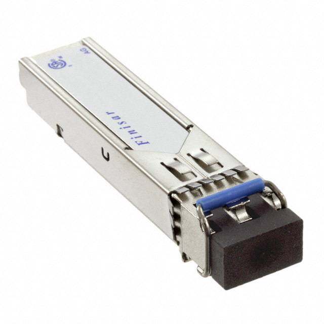
| 产品图片 |
|
| rohs | 符合RoHS无铅 / 符合限制有害物质指令(RoHS)规范要求 |
| 产品系列 | 光纤发射器、接收器、收发器,Avago Technologies AFCT-5805AZ- |
| mouser_ship_limit | 该产品可能需要其他文件才能进口到中国。 |
| 数据手册 | http://www.avagotech.com/docs/AV02-0807EN |
| 产品型号 | AFCT-5805AZ |
| 产品 | Transceivers |
| 产品种类 | 光纤发射器、接收器、收发器 |
| 其它名称 | 516-2355 |
| 商标 | Avago Technologies |
| 安装类型 | 通孔 |
| 工作电源电压 | 3.3 V, 5 V |
| 工厂包装数量 | 10 |
| 应用 | 通用 |
| 数据速率 | 155Mbps |
| 最大工作温度 | + 85 C |
| 最小工作温度 | - 40 C |
| 标准包装 | 10 |
| 波长 | 1300nm |
| 电压-电源 | * |
| 纤维类型 | Singlemode |
| 连接器类型 | SC |


- 商务部:美国ITC正式对集成电路等产品启动337调查
- 曝三星4nm工艺存在良率问题 高通将骁龙8 Gen1或转产台积电
- 太阳诱电将投资9.5亿元在常州建新厂生产MLCC 预计2023年完工
- 英特尔发布欧洲新工厂建设计划 深化IDM 2.0 战略
- 台积电先进制程称霸业界 有大客户加持明年业绩稳了
- 达到5530亿美元!SIA预计今年全球半导体销售额将创下新高
- 英特尔拟将自动驾驶子公司Mobileye上市 估值或超500亿美元
- 三星加码芯片和SET,合并消费电子和移动部门,撤换高东真等 CEO
- 三星电子宣布重大人事变动 还合并消费电子和移动部门
- 海关总署:前11个月进口集成电路产品价值2.52万亿元 增长14.8%


PDF Datasheet 数据手册内容提取
AFCT-5805xxxZ 155 Mb/s Single Mode Fiber Optic Transceiver for ATM, SONET OC-3/SDH STM-1 Data Sheet AFCT 5805AZ Description Features • 1300 nm Single mode transceiver for links up to 15 General Km The AFCT-5805xxxZ transceiver is a high performance, • Compliant with T1.646-1995 Broadband ISDN and cost effective module for serial optical data communica- T1E1.2/98-011R1 SONET network to customer tions applications specified for a data rate of 155 Mb/s. It installation interface standards is designed to provide a SONET/SDH compliant link for • Compliant with T1.105.06 SONET physical layer intermediate reach links operating at +3.3 V or +5.0 V specifications standard input voltage. • Multisourced 1 x 9 pin configuration Transmitter Section • Can replace LED multisourced 1 x 9 transceivers • Unconditionally eyesafe laser IEC 825/CDRH Class 1 The transmitter section of the AFCT-5805xxxZ consists compliant of a 1300 nm FP laser in an eyesafe optical subassembly • Integral duplex SC connector receptacle compatible (OSA) which mates to the fiber cable. The laser OSA is with TIA/EIA and IEC standards. driven by a custom IC which converts differential input PECL logic signals, ECL referenced (shifted) to +3.3 V or • RoHS compliant +5 V supply, into an analog laser drive current. • Two Temperature Ranges: AFCT-5805BZ/DZ 0°C to +70°C Receiver Section AFCT-5805AZ/CZ -40°C to +85°C AFCT-5805AMZ -40°C to +85°C The receiver utilizes an InGaAs PIN photodiode mounted AFCT-5805AEMZ -40°C to +85°C together with a transimpedance preamplifier IC in an OSA. This OSA is connected to a circuit providing post- amplifi- • Single +3.3 V or +5.0 V power supply operation cation quantization, and optical signal detection. • Wave solder and aqueous wash process compatible • Manufactured in an ISO 9002 certified facility • Considerable EMI margin to FCC Class B Applications • ATM 155 Mb/s links for LAN backbone switches and routers • ATM 155 Mb/s links for WAN core, edge and access switches and routers • ATM 155 Mb/s links for add/drop multiplexers and demultiplexers • SONET OC-3/SDH STM-1 (S-1.1) interconnections
ELECTRICAL SUBASSEMBLY PIN PHOTODIODE DATA PRE- DATA AMPLIFIER POST IC AMPLIFIER IC OPTICAL DUPLEX SC SUB- SIGNAL DETECT ASSEMBLIES RECEPTACLE DATA LASER DRIVER LASER DATA IC TOP VIEW Figure 1. Block Diagram Receiver Signal Detect Applications Information Signal Detect is a basic fiber failure indicator. This is a Typical BER Performance of Receiver versus Input Opti- single-ended PECL output. As the input optical power cal Power Level is decreased, Signal Detect will switch from high to low (deassert point) somewhere between sensitivity and The AFCT-5805xxxZ transceiver can be operated at the no light input level. As the input optical power is Bit-Error-Rate conditions other than the required BER = increased from very low levels, Signal Detect will switch 1 x 10⁻¹⁰ of the ATM Forum 155.52 Mb/s Physical Layer back from low to high (assert point). The assert level will be Standard. The typical trade-off of BER versus Relative In- at least 0.5 dB higher than the deassert level. put Optical Power is shown in Figure 2. The Relative Input Optical Power in dB is referenced to the actual sensitivity Transceiver Specified for Wide Temperature Range Op- of the device. For BER conditions better than 1 x 10⁻¹⁰, eration more input signal is needed (+dB). The AFCT-5805xxxZ is specified for operation over ex- 10-2 tended temperature range of -40° to +85°C. LINEAR EXTRAPOLATION OF 10-3 10-4 THROUGH 10-7 DATA Characterization of the parts has been performed over 10-4 BASED ON ACTUAL DATA the ambient operating temperature range in an airflow 10-5 O of 2 m/s. ATI 10-6 R R 10-7 Other Members of Avago Technologies SC Duplex RO 10-8 ER 10-9 155 Mb/s Product Family BIT 1100--1101 10-12 • HFCT-5801, 1300 nm single mode transceiver for 10-13 10-14 links up to 15 km. The part is based on the 2 x 9 in- 10-15 -5 -4 -3 -2 -1 0 1 2 3 dustry standard package and has laser bias, optical power monitor and transmitter disable functions. Figure 2. Relative Input Optical Power - dBm. Avg. 2
Recommended Circuit Schematic In order to ensure proper functionality of the AFCT- recommended, separate filter circuits shown in Figure 5805xxxZ a recommended circuit is provided in Figure 3 for the transmitter and receiver sections. These filter 3. When designing the circuit interface, there are a few circuits suppress VCC noise over a broad frequency range, fundamental guidelines to follow. For example, in the Rec- this prevents receiver sensitivity degradation due to VCC ommended Circuit Schematic figure the differential data noise. It is recommended that surface-mount compo- lines should be treated as 50 ohm Microstrip or stripline nents be used. Use tantalum capacitors for the 10 µF transmission lines. This will help to minimize the parasitic capacitors and monolithic, ceramic bypass capacitors for inductance and capacitance effects. Proper termination the 0.1 µF capacitors. Also, it is recommended that a sur- of the differential data signals will prevent reflections and face- mount coil inductor of 3.3 µH be used. Ferrite beads ringing which would compromise the signal fidelity and can be used to replace the coil inductors when using generate unwanted electrical noise. Locate termination quieter VCC supplies, but a coil inductor is recommended at the received signal end of the transmission line. The over a ferrite bead. All power supply components need to length of these lines should be kept short and of equal be placed physically next to the VCC pins of the receiver length. For the high speed signal lines, differential sig- and transmitter. Use a good, uniform ground plane with nals should be used, not single-ended signals, and these a minimum number of holes to provide a low-inductance differential signals need to be loaded symmetrically to ground current return for the power supply currents. prevent unbalanced currents from flowing which will In addition to these recommendations, Avago Tech- cause distortion in the signal. nologies Application Engineering staff is available for Maintain a solid, low inductance ground plane for re- consulting on best layout practices with various vendors turning signal currents to the power supply. Multilayer mux/demux, clock generator and clock recovery circuits. plane printed circuit board is best for distribution of VCC, Avago Technologies has participated in several reference returning ground currents, forming transmission lines design studies and is prepared to share the findings of and shielding, Also, it is important to suppress noise from these studies with interested customers. Contact your influencing the fiber-optic transceiver performance, es- local Avago Technologies sales representative to arrange pecially the receiver circuit. Proper power supply filtering for this service. of VCC for this transceiver is accomplished by using the NO INTERNAL NO INTERNAL CONNECTION CONNECTION TOP VIEW Rx Rx Tx Tx VEER RD RD SD VCCR VCCT TD TD VEET 1 2 3 4 5 6 7 8 9 NOTES: THE SPLIT-LOAD TERMINATIONS FOR PECL SIGNALS C1 C7 C2 C8 NEED TO BE LOCATED AT THE INPUT OF DEVICES RECEIVING THOSE PECL SIGNALS. V CC RECOMMEND 4-LAYER PRINTED CIRCUIT BOARD V L1 L2 R2 R3 WITH 50 Ω MICROSTRIP SIGNAL PATHS BE USED. CC C3 C4 TAETR PMHIYNATE R5 R7 V FILTER R1 C5 R4 FOR +5.0V AND +3.3V OPERATION. cc DINEPVUICTES C6 AT Vcc PINS R1 = R4 = R6 = R8 = R10 = 130 Ω TRANSCEIVER TERMINATION R2 = R3 = R5 = R7 = R9 = 82 Ω R6 R8 AT C1 = C2 = 10 µF R10 R9 TRANSCEIVER C3 = C4 = C7 = C8 = 100 nF INPUTS C5 = C6 = 0.1 µF L1 = L2 = 3.3 µH COIL OR FERRITE INDUCTOR. RD RD SD V TD TD CC Figure 3. Recommended Circuit Schematic 3
Evaluation Circuit Boards Recommended Solder and Wash Process Evaluation circuit boards are available from Avago Tech- The AFCT-5805xxxZ is compatible with industry standard nologies Application Engineering staff. Contact your local wave or hand solder processes. Avago Technologies sales representative to arrange for A drying cycle must be completed after wash process to access to one if needed. remove all moisture from the module. Recommended Solder Fluxes and Cleaning/Degreasing AFCT-5805xxxZ Process Plug Chemicals The AFCT-5805xxxZ transceiver is supplied with a process Solder fluxes used with the AFCT-5805xxxZ fiber-optic plug for protection of the optical ports with the Duplex transceiver should be water-soluble, organic solder flux- SC connector receptacle. This process plug prevents con- es. Some recommended solder fluxes are Lonco 3355-11 tamination during wave solder and aqueous rinse as well from London Chemical West, Inc. of Burbank, CA, and 100 as during handling, shipping or storage. Each process Flux from Alpha Metals of Jersey City, NJ. plug can only be used once during processing, although Recommended cleaning and degreasing chemicals for the with subsequent use, it can be used as a dust cover. It is AFCT-5805xxxZ are alcohol’s (methyl, isopropyl, isobutyl), made of high-temperature, molded, sealing material that aliphatics (hexane, heptane) and other chemicals, such as will withstand +85°C and a rinse pressure of 110 lb/in2. soap solution or naphtha. Do not use partially halogenated hydrocarbons for cleaning/degreasing. Examples of chemi- cals to avoid are 1.1.1. trichloroethane, ketones (such as MEK), acetone, chloroform, ethyl acetate, methylene dichlo- ride, phenol, methylene chloride or N-methylpyrrolidone. 20.32 2 x Ø 1.9 ± 0.1 (0.800) (0.075 ± 0.004) 9 x Ø 0.8 ± 0.1 20.32 (0.032 ± 0.004) (0.800) 2.54 (0.100) TOP VIEW DIMENSIONS ARE IN MILLIMETERS (INCHES) Figure 4. Recommended Board Layout Hole Pattern 4
AVAGO XXXX-XXXX KEY: ZZZZZ LASER PROD 21CFR(J) CLASS 1 YYWW = DATE CODE COUNTRY OF ORIGIN YYWW XXXX-XXXX = AFCT-5815 ZZZZ = 1300 nm TX RX MAX 39.6 12.7 . (1.56) (0.50) AREA RESERVED 25.4 MAX. FOR 12.7 ± 0.3 (1.00) PROCESS (0.50 ± 0.012) PLUG 2.0 ± 0.1 2.5 SLOT WIDTH SLOT DEPTH (0.079 ± 0.004) +0.1 (0.10) 0.25 -0.05 ( +0.004) 0.010 -0.002 9.8 MAX. (0.386) 0.51 3.3 ± 0.38 (0.020) (0.130 ± 0.015) +0.25 20.32 ± 0.2 15.8 ± 0.15 0.46 -0.05 (0.800 ± 0.008) (0.622 ± 0.006) 9 x Ø ( +0.010) 1.27 +0.25 0.018 -0.05 -0.002 2 x Ø ( +0.010) 0.050 -0.002 23.8 20.32 8 x 2.54 20.32 ± 0.2 (0.937) (0.800) (0.100) (0.800 ± 0.008) 1.3 2 x Ø (0.051) DIMENSIONS ARE IN MILLIMETERS (INCHES). TOLERANCES: ±0.1 mm UNLESS OTHERWISE SPECIFIED. Figure 5. Package Outline Drawing and Pinout 5
Regulatory Compliance Electromagnetic Interference (EMI) The AFCT-5805xxxZ is intended to enable commercial Most equipment designs utilizing these high-speed system designers to develop equipment that complies transceivers from Avago Technologies will be required with the various regulations governing certification of to meet the requirements of FCC in the United States, Information Technology Equipment. See the Regulatory CENELEC EN55022 (CISPR 22) in Europe and VCCI in Compliance Table 1 for details. Additional information is Japan. available from your Avago Technologies sales represen- The AFCT-5805xxxZ has been characterized without a tative. chassis enclosure to demonstrate the robustness of the Electrostatic Discharge (ESD) part’s integral shielding. Performance of a system con- taining these transceivers within a well designed chassis There are two design cases in which immunity to ESD is expected to be better than the results of these tests damage is important. with no chassis enclosure. The first case is during handling of the transceiver prior Immunity to mounting it on the circuit board. It is important to use normal ESD handling precautions for ESD sensitive Equipment utilizing these AFCT-5805xxxZ transceivers devices. These precautions include using grounded wrist will be subject to radio-frequency electromagnetic fields straps, work benches and floor mats in ESD controlled in some environments. These transceivers, with their inte- areas. gral shields, have been characterized without the benefit of a normal equipment chassis enclosure and the results The second case to consider is static discharges to the are reported below. Performance of a system contain- exterior of the equipment chassis containing the trans- ing these transceivers within a well designed chassis ceiver parts. To the extent that the duplex SC connector is expected to be better than the results of these tests is exposed to the outside of the equipment chassis it may without a chassis enclosure. be subject to whatever ESD system level test criteria that the equipment is intended to meet. 6
Table 1. Regulatory Compliance - Typical Performance Feature Test Method Performance Electrostatic MII-STD-883F Class 1 (>500 V) - Human Body Model Discharge (ESD) to Method 3015.7 the Electrical Pins Electrostatic Variation of Air discharge 15 kV Discharge (ESD) IEC 61000-4-2 to the Duplex SC Receptacle Electromagnetic FCC Class B Typically provide greater than 11 dB margin below 1 Interference (EMI) GHz to FCC Class B when tested in a GTEM with the transceiver mounted to a circuit card without a chassis enclosure at frequencies up to 1 GHz. Margins above 1 GHz dependent on customer board and chassis designs. Immunity Variation of IEC 801-3 Typically show no measurable effect from a 10 V/m field swept from 27 MHz to 1 GHz applied to the transceiver without a chassis enclosure. Eye Safety FDA CDRH 21-CFR 1040 Class 1 Accession Number: 9521220-121 IEC 60825 - 1 TUV Approved Component Underwriters Laboratories and Canadian UL File#: E173874 Recognition Standards Association Joint Component Recognition for Information Technology Equipment Including Electrical Performance Specifications Absolute Maximum Ratings Stresses in excess of the absolute maximum ratings can cause catastrophic damage to the device. Limits apply to each parameter in isolation, all other parameters having values within the recommended operating conditions. It should not be assumed that limiting values of more than one parameter can be applied to the product at the same time. Exposure to the absolute maximum ratings for extended periods can adversely affect device reliability. Parameter Symbol Minimum Maximum Units Notes Storage Temperature TS -40 +85 °C Lead Soldering Temperature/Time - - +260/10 °C/s Input Voltage - GND VCC V Power Supply Voltage - 0 6 V Operating Environment Parameter Symbol Minimum Maximum Units Notes Power Supply Voltage VCC +3.1 +5.25 V Ambient Operating Temperature - AFCT-5805AZ/CZ/AMZ TOP -40 +85 °C 1 Ambient Operating Temperature - AFCT-5805BZ/DZ TOP 0 +70 °C 1 7
Transmitter Section (Ambient Operating Temperature, VCC = 3.1 V to 5.25 V) Parameter Symbol Minimum Typical Maximum Units Notes Output Center Wavelength lce 1261 - 1360 Output Spectral Width (RMS) Dl - - 7.7 nm Average Optical Output Power PO -15 - -8 dBm 2 Extinction Ratio ER 8.2 - - dB Power Supply Current ICC - 50 140 mA 3 Output Eye Compliant with Telcordia TR-NWT-000253 and ITU recommendation G.957 Optical Rise Time tR - - 2 ns 4 Optical Fall Time tF - - 2 ns 4 Data Input Current - Low IIL -350 - - µA Data Input Current - High IIH - - 350 µA Data Input Voltage - Low VIL - VCC -2.0 - -1.475 V 5 Data Input Voltage - High VIH - VCC -1.165 - -0.74 V 5 Notes: 1. 2 m/s air flow required. 2. Output power is power coupled into a single mode fiber. 3. The power supply current varies with temperature. Maximum current is specified at VCC = Maximum @ maximum temperature (not including terminations) and end of life. Typical power supply current at +25°C and +3.3 V or +5.0 V supply. 4. 10% - 90% Values. Maximum tR, tF times tested against eye mask. 5. These inputs are compatible with 10 K, 10 KH and 100 K PECL outputs. Receiver Section (Ambient Operating Temperature, VCC = 3.1 V to 5.25 V) Parameter Symbol Minimum Typical Maximum Units Notes Receiver Sensitivity - - - -31 dBm 6 Maximum Input Power - -7 - - dBm 6 Power Supply Current ICC - 55 100 mA 7 Signal Detect - Deasserted - -45 - -31 dBm Signal Detect - Hysteresis - 0.5 - 4 dB Signal Detect Assert Time AS_Max - - 100 µs (off to on) Signal Detect Deassert Time ANS_Max - - 350 µs (on to off) Signal Detect Output Voltage - Low VOL - VCC -1.92 - -1.45 V 8 Signal Detect Output Voltage - High VOH - VCC -1.1 - -0.85 V 8 Data Output Voltage - Low VOL - VCC -2.0 - -1.45 V 8 Data Output Voltage - High VOH - VCC -1.1 - -0.85 V 8 Data Output Rise Time tr - - 2.2 ns 9 Data Output Fall Time tf - - 2.2 ns 9 Notes 6. Sensitivity and maximum input power levels for a 223-1 PRBS with 72 ones and 72 zeros inserted. (ITU recommendation G.958). 7. The current includes capacitively coupled 50 Ohm terminations. 8. These outputs are compatible with 10 K, 10 KH and 100 K PECL outputs. 9. 20 - 80% levels. 8
Table 2. Pin Out Table Pin Symbol Functional Description Mounting Studs The mounting studs are provided for transceiver mechanical attachment to the circuit board. They are embedded in the housing and are not connected to the transceiver internal circuit. They should be soldered into plated-through holes on the printed circuit board. 1 VEER Receiver Signal Ground Directly connect this pin to receiver signal ground plane. 2 RD+ Receiver Data Out Terminate this high-speed, differential, PECL output with standard PECL techniques at the follow-on device input pin. 3 RD- Receiver Data Out Bar Terminate this high-speed, differential, PECL output with standard PECL techniques at the follow-on device input pin. 4 SD Signal Detect Normal input optical levels to the receiver result in a logic “1” output. Low input optical levels to the receiver result in a fault indication shown by a logic “0” output. Signal Detect is a single-ended, PECL output. This output will operate with 270 Ω termination resistor to VEE to achieve PECL output levels. This Signal Detect output can be used to drive a PECL input on an upstream circuit, such as, Signal Detect input and Loss of Signal-bar input. 5 VCCR Receiver Power Supply Provide +3.3 or +5.0 V dc via the recommended receiver power supply filter circuit. Locate the power supply filter circuit as close as possible to the VCCR pin. 6 VCCT Transmitter Power Supply Provide +3.3 or +5.0 V dc via the recommended transmitter power supply filter circuit. Locate the power supply filter circuit as close as possible to the VCCT pin. 7 TD- Transmitter Data In Bar Terminate this high-speed, differential Transmitter Data input with standard PECL techniques at the transmitter input pin. 8 TD+ Transmitter Data In Terminate this high-speed, differential Transmitter Data input with standard PECL techniques at the transmitter input pin. 9 VEET Transmitter Signal Ground Directly connect this pin to the transmitter signal ground plane. 9
Order Information: Temperature Range 0°C to +70°C AFCT-5805BZ Black Case AFCT-5805DZ Blue Case Temperature Range -40°C to +85°C AFCT-5805AZ Black Case AFCT-5805CZ Blue Case AFCT-5805AMZ Metalized Housing AFCT-5805AEMZ Metalized Housing with E-shield Class 1 Laser Product: This product conforms to the applicable requirements of 21 CFR 1040 at the date of manufacture Date of Manufacture: Avago Technologies Inc., No 1 Yishun Ave 7, Singapore Handling Precautions 1. The AFCT-5805xxxZ can be damaged by current surges or overvoltage. Power supply transient precautions should be taken. 2. Normal handling precautions for electrostatic sensitive devices should be taken. For product information and a complete list of distributors, please go to our web site: www.avagotech.com Avago, Avago Technologies, and the A logo are trademarks of Avago Technologies in the United States and other countries. Data subject to change. Copyright © 2005-2014 Avago Technologies. All rights reserved. Obsoletes AV01-0034EN AV02-0807EN - December 9, 2014