 Datasheet下载
- 型号: ADUM3160BRWZ-RL
- 制造商: Analog
- 库位|库存: xxxx|xxxx
- 要求:
| 数量阶梯 | 香港交货 | 国内含税 |
| +xxxx | $xxxx | ¥xxxx |
查看当月历史价格
查看今年历史价格
ADUM3160BRWZ-RL产品简介:
ICGOO电子元器件商城为您提供ADUM3160BRWZ-RL由Analog设计生产,在icgoo商城现货销售,并且可以通过原厂、代理商等渠道进行代购。 ADUM3160BRWZ-RL价格参考。AnalogADUM3160BRWZ-RL封装/规格:数字隔离器, USB Digital Isolator 2500Vrms 2 Channel 12Mbps 25kV/µs CMTI 16-SOIC (0.295", 7.50mm Width)。您可以下载ADUM3160BRWZ-RL参考资料、Datasheet数据手册功能说明书,资料中有ADUM3160BRWZ-RL 详细功能的应用电路图电压和使用方法及教程。
ADUM3160BRWZ-RL是Analog Devices Inc.(亚德诺半导体)推出的一款高性能数字隔离器,主要用于实现USB接口的信号隔离。该器件集成了iCoupler®磁隔离技术,能够在高速数据传输的同时提供可靠的电气隔离,广泛应用于需要隔离保护和抗干扰能力的工业与医疗电子系统中。

典型应用场景包括:工业自动化控制系统中的USB通信隔离,防止高电压或噪声干扰影响主机设备;医疗设备中用于隔离患者连接部分与主控电路,以满足安全标准要求;嵌入式系统中通过隔离延长USB总线的可靠性和安全性;以及在测试测量仪器、电源管理系统中用于实现接地隔离,避免地环路干扰。

ADUM3160BRWZ-RL支持USB 2.0全速(12 Mbps)通信,具备低功耗、高共模瞬态抗扰度和优于光耦的长期可靠性,采用小型SOIC-16封装,适合空间受限的应用。其无需外部隔离电源的特点也简化了系统设计。总体而言,该器件适用于对安全性、稳定性和抗干扰能力要求较高的工业、医疗及通信领域。
| 参数 | 数值 |
| 产品目录 | |
| ChannelType | 双向 |
| 描述 | IC DGTL ISO 4CH LOGIC 16SOIC数字隔离器 Full/Low Spd USB 2.0 Digital |
| 产品分类 | |
| IsolatedPower | 无 |
| 品牌 | Analog Devices Inc |
| 产品手册 | |
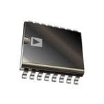
| 产品图片 |
|
| rohs | 符合RoHS无铅 / 符合限制有害物质指令(RoHS)规范要求 |
| 产品系列 | 接口 IC,数字隔离器,Analog Devices ADUM3160BRWZ-RLiCoupler® |
| 数据手册 | |
| 产品型号 | ADUM3160BRWZ-RL |
| PCN设计/规格 | |
| PulseWidthDistortion(Max) | - |
| 上升/下降时间(典型值) | 20ns, 20ns (最小值) |
| 产品培训模块 | http://www.digikey.cn/PTM/IndividualPTM.page?site=cn&lang=zhs&ptm=25559 |
| 产品种类 | |
| 传播延迟tpLH/tpHL(最大值) | 70ns, 70ns |
| 传播延迟时间 | 70 ns |
| 供应商器件封装 | 16-SOIC W |
| 共模瞬态抗扰度(最小值) | 25kV/µs |
| 其它名称 | ADUM3160BRWZ-RL-ND |
| 包装 | 带卷 (TR) |
| 商标 | Analog Devices |
| 安装风格 | SMD/SMT |
| 封装 | Reel |
| 封装/外壳 | 16-SOIC(0.295",7.50mm 宽) |
| 封装/箱体 | SOIC-16 |
| 工作温度 | -40°C ~ 105°C |
| 工厂包装数量 | 1000 |
| 技术 | 磁耦合 |
| 数据速率 | 12Mbps |
| 最大工作温度 | + 105 C |
| 最大数据速率 | 12 Mb/s |
| 最小工作温度 | - 40 C |
| 标准包装 | 1,000 |
| 电压-电源 | 3 V ~ 5.5 V |
| 电压-隔离 | 2500Vrms |
| 电源电压-最大 | 5.5 V |
| 电源电压-最小 | 4 V |
| 类型 | USB |
| 系列 | ADUM3160 |
| 绝缘电压 | 2.5 kVrms |
| 脉宽失真(最大) | - |
| 视频文件 | http://www.digikey.cn/classic/video.aspx?PlayerID=1364138032001&width=640&height=505&videoID=2219593469001http://www.digikey.cn/classic/video.aspx?PlayerID=1364138032001&width=640&height=505&videoID=2219593470001http://www.digikey.cn/classic/video.aspx?PlayerID=1364138032001&width=640&height=505&videoID=2219614223001 |
| 输入-输入侧1/输入侧2 | 2/2 |
| 通道数 | 4 |
| 通道数量 | 4 Channel |
| 通道类型 | 双向 |
| 隔离式电源 | 无 |


- 商务部:美国ITC正式对集成电路等产品启动337调查
- 曝三星4nm工艺存在良率问题 高通将骁龙8 Gen1或转产台积电
- 太阳诱电将投资9.5亿元在常州建新厂生产MLCC 预计2023年完工
- 英特尔发布欧洲新工厂建设计划 深化IDM 2.0 战略
- 台积电先进制程称霸业界 有大客户加持明年业绩稳了
- 达到5530亿美元!SIA预计今年全球半导体销售额将创下新高
- 英特尔拟将自动驾驶子公司Mobileye上市 估值或超500亿美元
- 三星加码芯片和SET,合并消费电子和移动部门,撤换高东真等 CEO
- 三星电子宣布重大人事变动 还合并消费电子和移动部门
- 海关总署:前11个月进口集成电路产品价值2.52万亿元 增长14.8%


PDF Datasheet 数据手册内容提取
Full/Low Speed 2.5 kV USB Digital Isolator Data Sheet ADuM3160 FEATURES GENERAL DESCRIPTION USB 2.0 compatible The ADuM31601 is a USB port isolator based on Analog Low and full speed data rate: 1.5 Mbps and 12 Mbps Devices, Inc., iCoupler® technology. Combining high speed CMOS Bidirectional communication and monolithic air core transformer technology, this isolation 4.5 V to 5.5 V VBUS operation component provides outstanding performance characteristics 7 mA maximum upstream supply current at 1.5 Mbps and is easily integrated with low and full speed USB-compatible 8 mA maximum upstream supply current at 12 Mbps peripheral devices. 2.3 mA maximum upstream idle current Many microcontrollers implement USB so that it presents only the Upstream short-circuit protection D+ and D− lines to external pins. This is desirable in many cases Class 3A contact ESD performance per ANSI/ESD STM5.1-2007 because it minimizes external components and simplifies the High temperature operation: 105°C design; however, this presents particular challenges when isolation High common-mode transient immunity: >25 kV/μs is required. Because the USB lines must switch between actively 16-lead SOIC wide body package driving D+/D− and allowing external resistors to set the state of RoHS compliant the bus, the ADuM3160 provides mechanisms for detecting the Qualified for automotive applications direction of data flow and control over the state of the output Safety and regulatory approvals buffers. Data direction is determined on a packet-by-packet basis. UL recognition: 2500 V rms for 1 minute per UL 1577 CSA Component Acceptance Notice #5A The ADuM3160 uses the edge detection based iCoupler IEC 60950-1: 600 V rms (basic) technology in conjunction with internal logic to implement VDE certificate of conformity a transparent, easily configured, upstream-facing port isolator. DIN V VDE V 0884-10 (VDE V 0884-10):2006-12 Isolating the upstream port provides several advantages in V = 560 V peak simplicity, power management, and robust operation. IORM APPLICATIONS The isolator has a propagation delay comparable to that of a standard hub and cable. It operates with the bus voltage on either USB peripheral isolation side ranging from 4.5 V to 5.5 V, allowing connection directly to Isolated USB hub V by internally regulating the voltage to the signaling level. BUSx The ADuM3160 provides isolated control of the pull-up resistor to allow the peripheral to control connection timing. The device draws low enough idle current that a suspend state is not required. A 5 kV, reinforced insulation version, the ADuM4160, is available. FUNCTIONAL BLOCK DIAGRAM VBUS1 1 REG REG 16VBUS2 GND1 2 15GND2 VDD1 3 14VDD2 PDEN 4 13SPD SPU 5 12PIN UD– 6 11DD– UD+ 7 10DD+ GND1 8 PU LOGIC PD LOGIC 9 GND2 09125-001 Figure 1. 1 Protected by U.S. Patents 5,952,849; 6,873,065; 7,075,329; and 8,432,812. Rev. C Document Feedback Information furnished by Analog Devices is believed to be accurate and reliable. However, no responsibility is assumed by Analog Devices for its use, nor for any infringements of patents or other One Technology Way, P.O. Box 9106, Norwood, MA 02062-9106, U.S.A. rights of third parties that may result from its use. Specifications subject to change without notice. No license is granted by implication or otherwise under any patent or patent rights of Analog Devices. Tel: 781.329.4700 ©2010–2014 Analog Devices, Inc. All rights reserved. Trademarks and registered trademarks are the property of their respective owners. Technical Support www.analog.com
ADuM3160 Data Sheet TABLE OF CONTENTS Features .............................................................................................. 1 ESD Caution...................................................................................6 Applications ....................................................................................... 1 Pin Configuration and Function Descriptions ..............................7 General Description ......................................................................... 1 Applications Information .................................................................9 Functional Block Diagram .............................................................. 1 Functional Description .................................................................9 Revision History ............................................................................... 2 Product Usage ................................................................................9 Specifications ..................................................................................... 3 Compatibility of Upstream Applications ................................ 10 Electrical Characteristics ............................................................. 3 Power Supply Options ............................................................... 10 Package Characteristics ............................................................... 4 Printed Circuit Board Layout ................................................... 10 Regulatory Information ............................................................... 4 DC Correctness and Magnetic Field Immunity ..................... 10 Insulation and Safety-Related Specifications ............................ 4 Insulation Lifetime ..................................................................... 11 DIN V VDE V 0884-10 (VDE V 0884-10) Insulation Outline Dimensions ....................................................................... 13 Characteristics .............................................................................. 5 Ordering Guide .......................................................................... 13 Recommended Operating Conditions ...................................... 5 Automotive Products ................................................................. 13 Absolute Maximum Ratings ............................................................ 6 REVISION HISTORY 3/14—Rev. B to Rev. C 9/10—Rev. 0 to Rev. A Change to Features Section ............................................................. 1 Changes to Data Sheet Title, Features, Applications, Added Patent ..................................................................................... 1 and General Description; Added USB Logo .................................. 1 Change to Switching Specifications, I/O Pins, Full Speed Changes to Electrical Characteristics Section and Table 1 .......... 3 Parameter, Table 1 ............................................................................. 3 Changes to Table 2 and Table 3, Endnote 1 ................................... 4 Changes to Ordering Guide .......................................................... 13 Changes to Table 5 ............................................................................. 5 Added Automotive Products Section .......................................... 13 Changes to Table 9 ............................................................................. 8 Changes to Table 10 .......................................................................... 9 3/13—Rev. A to Rev. B Changes to Functional Description Section ............................... 10 Created Hyperlink for Safety and Regulatory Approvals Changes to Product Usage Section .............................................. 10 Entry in Features Section ................................................................. 1 Added Compatibility of Upstream Applications Section .......... 11 Changes to General Description Section and Figure 1 ............... 1 Changes to Power Supply Options Section and Change to Table 8 ............................................................................. 6 DC Correctness and Magnetic Field Immunity Section ........... 11 Changes to Figure 3 and Table 9 ..................................................... 7 Changes to Functional Description Section ................................. 9 7/10—Revision 0: Initial Version Updated Outline Dimensions ....................................................... 13 Rev. C | Page 2 of 16
Data Sheet ADuM3160 SPECIFICATIONS ELECTRICAL CHARACTERISTICS 4.5 V ≤ V ≤ 5.5 V, 4.5 V ≤ V ≤ 5.5 V; 3.1 V ≤ V ≤ 3.6 V, 3.1 V ≤ V ≤ 3.6 V. All minimum/maximum specifications apply over BUS1 BUS2 DD1 DD2 the entire recommended operation range, unless otherwise noted; all typical specifications are at T = 25°C, V = V = 3.3 V. All A DD1 DD2 voltages are relative to their respective grounds. Table 1. Parameter Symbol Min Typ Max Unit Test Conditions/Comments1 DC SPECIFICATIONS Total Supply Current2 1.5 Mbps 750 kHz logic signal rate, C = 450 pF L V or V Supply Current I 5 7 mA DD1 BUS1 DD1 (L) V or V Supply Current I 5 7 mA DD2 BUS2 DD2 (L) 12 Mbps 6 MHz logic signal rate, C = 50 pF L V or V Supply Current I 6 8 mA DD1 BUS1 DD1 (F) V or V Supply Current I 6 8 mA DD2 BUS2 DD2 (F) Idle Current V or V Idle Current I 1.7 2.3 mA DD1 BUS1 DD1 (I) Input Currents I , I , −1 +0.1 +1 µA 0 V ≤ V , V , V , V , V , V , DD− DD+ DD− DD+ UD+ UD− SPD PIN I , I , V , V ≤ 3.0 V UD+ UD− SPU PDEN I , I , SPD PIN I , I SPU PDEN Single-Ended Logic High Input Threshold V 2.0 V IH Single-Ended Logic Low Input Threshold V 0.8 V IL Single-Ended Input Hysteresis V 0.4 V HST Differential Input Sensitivity V 0.2 V |V − V | DI XD+ XD− Logic High Output Voltages V 2.8 3.6 V R = 15 kΩ, V = 0 V OH L L Logic Low Output Voltages V 0 0.3 V R = 1.5 kΩ, V = 3.6 V OL L L V and V Supply Undervoltage Lockout V 2.4 3.1 V DD1 DD2 UVLO V Supply Undervoltage Lockout V 3.5 4.35 V BUS1 UVLOB1 V Supply Undervoltage Lockout V 3.5 4.4 V BUS2 UVLOB2 Transceiver Capacitance C 10 pF UD+, UD−, DD+, DD− to ground IN Capacitance Matching 10 % Full Speed Driver Impedance Z 4 20 Ω OUTH Impedance Matching 10 % SWITCHING SPECIFICATIONS, I/O PINS, LOW SPEED Low Speed Data Rate 1.5 Mbps C = 50 pF L Propagation Delay3 t , t 325 ns C = 50 pF, SPD = SPU = low, PHL PLH L V , V = 3.3 V DD1 DD2 Side 1 Output Rise/Fall Time (10% to 90%), t , t 75 300 ns C = 450 pF, SPD = SPU = low, RL FL L Low Speed V , V = 3.3 V DD1 DD2 Low Speed Differential Jitter, Next Transition |t | 45 ns C = 50 pF LJN L Low Speed Differential Jitter, Paired Transition |t | 15 ns C = 50 pF LJP L SWITCHING SPECIFICATIONS, I/O PINS, FULL SPEED Maximum Data Rate 12 Mbps C = 50 pF L Propagation Delay3 t , t 20 60 70 ns C = 50 pF, SPD = SPU = high, PHL PLH L V , V = 3.3 V DD1 DD2 Output Rise/Fall Time (10% to 90%), Full Speed t , t 4 20 ns C = 50 pF, SPD = SPU = high, RF FF L V , V = 3.3 V DD1 DD2 Full Speed Differential Jitter, Next Transition |t | 3 ns C = 50 pF HJN L Full Speed Differential Jitter, Paired Transition |t | 1 ns C = 50 pF HJP L Rev. C | Page 3 of 16
ADuM3160 Data Sheet Parameter Symbol Min Typ Max Unit Test Conditions/Comments1 For All Operating Modes Common-Mode Transient Immunity |CM | 25 35 kV/µs V , V , V , V = V or V , H UD+ UD− DD+ DD− DD1 DD2 at Logic High Output4 V = 1000 V, transient magnitude = CM 800 V Common-Mode Transient Immunity |CM| 25 35 kV/µs V , V , V , V = 0 V, V = L UD+ UD− DD+ DD− CM at Logic Low Output4 1000 V, transient magnitude = 800 V 1 CL = load capacitance, RL = test load resistance, VL = test load voltage, and VCM = common-mode voltage. 2 The supply current values are for the device running at a fixed continuous data rate 50% duty cycle, alternating J and K states. Supply current values are specified with USB-compliant load present. 3 Propagation delay of DD+ to UD+ or DD− to UD− in either signal direction is measured from the 50% level of the rising or falling edge to the 50% level of the rising or falling edge of the corresponding output signal. 4 CMH is the maximum common-mode voltage slew rate that can be sustained while maintaining VO > 0.8 VDD2. CML is the maximum common-mode voltage slew rate that can be sustained while maintaining VO < 0.8 V. The common-mode voltage slew rates apply to both rising and falling common-mode voltage edges. The transient magnitude is the range over which the common mode is slewed. PACKAGE CHARACTERISTICS Table 2. Parameter Symbol Min Typ Max Unit Test Conditions/Comments Resistance (Input to Output)1 R 1012 Ω I-O Capacitance (Input to Output)1 C 2.2 pF f = 1 MHz I-O Input Capacitance2 C 4.0 pF I IC Junction-to-Ambient Thermal Resistance θ 45 °C/W Thermocouple located at center of JA package underside 1 The device is considered a 2-terminal device; Pin 1 through Pin 8 are shorted together, and Pin 9 through Pin 16 are shorted together. 2 Input capacitance is from any input data pin to ground. REGULATORY INFORMATION The ADuM3160 has been approved by the organizations listed in Table 3. For more information about the recommended maximum working voltages for specific cross-insulation waveforms and insulation levels, see Table 8 and the Insulation Lifetime section. Table 3. UL CSA VDE Recognized under UL 1577 component Approved under CSA Component Acceptance Notice #5A Certified according to DIN V VDE V recognition program1 0884-10 (VDE V 0884-10):2006-122 Single protection, 2500 V rms isolation Basic insulation per CSA 60950-1-07 and IEC 60950-1, Reinforced insulation, 560 V peak voltage 600 V rms (849 V peak) maximum working voltage File E214100 File 205078 File 2471900-4880-0001 1 In accordance with UL 1577, each ADuM3160 is proof tested by applying an insulation test voltage ≥ 3000 V rms for 1 sec (current leakage detection limit = 10 µA). 2 In accordance with DIN V VDE V 0884-10 (VDE V 0884-10):2006-12, each ADuM3160 is proof tested by applying an insulation test voltage ≥ 1050 V peak for 1 sec (partial discharge detection limit = 5 pC). The asterisk (*) marking branded on the component indicates DIN V VDE V 0884-10 (VDE V 0884-10):2006-12 approval. INSULATION AND SAFETY-RELATED SPECIFICATIONS Table 4. Parameter Symbol Value Unit Test Conditions/Comments Rated Dielectric Insulation Voltage 2500 V 1 minute duration Minimum External Air Gap (Clearance) L(I01) 8.0 min mm Measured from input terminals to output terminals, shortest distance through air Minimum External Tracking (Creepage) L(I02) 7.7 min mm Measured from input terminals to output terminals, shortest distance path along body Minimum Internal Gap (Internal Clearance) 0.017 min mm Insulation distance through insulation Tracking Resistance (Comparative Tracking Index) CTI >175 V DIN IEC 112/VDE 0303, Part 1 Isolation Group IIIa Material Group (DIN VDE 0110, 1/89, Table 1) Rev. C | Page 4 of 16
Data Sheet ADuM3160 DIN V VDE V 0884-10 (VDE V 0884-10) INSULATION CHARACTERISTICS This isolator is suitable for reinforced electrical isolation only within the safety limit data. Maintenance of the safety data is ensured by protective circuits. The asterisk (*) marking branded on the component denotes DIN V VDE V 0884-10 (VDE V 0884-10):2006-12 approval. Table 5. Description Test Conditions/Comments1 Symbol Characteristic Unit Installation Classification per DIN VDE 0110 For Rated Mains Voltage ≤ 150 V rms I to IV For Rated Mains Voltage ≤ 300 V rms I to III For Rated Mains Voltage ≤ 400 V rms I to II Climatic Classification 40/105/21 Pollution Degree per DIN VDE 0110, Table 1 2 Maximum Working Insulation Voltage V 560 V peak IORM Input-to-Output Test Voltage, Method B1 V × 1.875 = V , 100% production test, t = 1 sec, V 1050 V peak IORM PR m PR partial discharge < 5 pC Input-to-Output Test Voltage, Method A V PR After Environmental Tests Subgroup 1 V × 1.6 = V , t = 60 sec, partial discharge < 5 pC 896 V peak IORM PR m After Input and/or Safety Tests V × 1.2 = V , t = 60 sec, partial discharge < 5 pC 672 V peak IORM PR m Subgroup 2 and Subgroup 3 Highest Allowable Overvoltage Transient overvoltage, t = 10 seconds V 4000 V peak TR TR Safety-Limiting Values Maximum value allowed in the event of a failure (see Figure 2) Case Temperature T 150 °C S Side 1 + Side 2 Current I 550 mA S1 Insulation Resistance at T V = 500 V R >109 Ω S IO S 1 For information about tM, tTR, and VIO, see DIN V VDE V 0884-10. 600 RECOMMENDED OPERATING CONDITIONS A) Table 6. m500 T ( Parameter Symbol Min Max Unit N E R Operating Temperature T −40 +105 °C R400 A U V CDD1300 SInuppuptl yS iVgonlatal gReisse1 and Fall V BUS1, VBUS2 3 .0 51..50 Vm s G Times N ERATI200 1 All voltages are relative to their respective grounds. See the DC Correctness OP and Magnetic Field Immunity section for information about immunity to E external magnetic fields. F100 A S 00 50AMBIENTTEM1P00ERATURE(°C1)50 200 09125-002 Figure 2. Thermal Derating Curve, Dependence of Safety-Limiting Values on Case Temperature, per DIN V VDE V 0884-10 Rev. C | Page 5 of 16
ADuM3160 Data Sheet ABSOLUTE MAXIMUM RATINGS Ambient temperature = 25°C, unless otherwise noted. Stresses above those listed under Absolute Maximum Ratings may cause permanent damage to the device. This is a stress Table 7. rating only; functional operation of the device at these or any Parameter Rating other conditions above those indicated in the operational Storage Temperature (T ) −40°C to +150°C ST section of this specification is not implied. Exposure to absolute Ambient Operating Temperature (T ) −40°C to +105°C A maximum rating conditions for extended periods may affect Supply Voltages (V , V , V , −0.5 V to +6.5 V BUS1 BUS2 DD1 V )1, 2 device reliability. DD2 Input Voltage (V , V , V )1 −0.5 V to V + 0.5 V UD+ UD− SPU DD1 Output Voltage (VDD−, VDD+, VSPD, VPIN)1 −0.5 V to VDD2 + 0.5 V ESD CAUTION Average Output Current per Pin3 Side 1 (I ) −10 mA to +10 mA O1 Side 2 (I ) −10 mA to +10 mA O2 Common-Mode Transients4 −100 kV/µs to +100 kV/µs 1 All voltages are relative to their respective grounds. 2 VDD1, VDD2, VBUS1, and VBUS2 refer to the supply voltages on the input and output sides of a given channel, respectively. 3 See Figure 2 for maximum rated current values for various temperatures. 4 Refers to common-mode transients across the insulation barrier. Common- mode transients exceeding the Absolute Maximum Ratings may cause latch-up or permanent damage. Table 8. Maximum Continuous Working Voltage1 Parameter Max Unit Constraint AC Voltage, Bipolar Waveform Basic Insulation 560 V peak 50-year minimum lifetime AC Voltage, Unipolar Waveform Basic Insulation 849 V peak Maximum approved working voltage per IEC 60950-1 DC Voltage Basic Insulation 849 V peak Maximum approved working voltage per IEC 60950-1 1 Refers to continuous voltage magnitude imposed across the isolation barrier. See the Insulation Lifetime section for more information. Rev. C | Page 6 of 16
Data Sheet ADuM3160 PIN CONFIGURATION AND FUNCTION DESCRIPTIONS VBUS1 1 16 VBUS2 GND1* 2 15 GND2* VDD1 3 14 VDD2 ADuM3160 PDEN 4 13 SPD TOP VIEW SPU 5 (Not to Scale) 12 PIN UD– 6 11 DD– UD+ 7 10 DD+ GND1* 8 9 GND2* *PIN 2AND PIN 8ARE INTERNALLY CONNECTEDTO EACH OTHER,AND IT IPISSI N RR E9ECCAOONMMD MMPEEINNN 1DD5EEADDR TTEHH IAANTTT BBEROONTTAHHL PPLIIYNN SSC OBBNEE NCCEOOCNNTNNEEEDCCTTTOEE DDEATTOOCH AA OCCTOOHMMEMMROO,ANNN GGDRR ITOOUUNNDD..09125-003 Figure 3. Pin Configuration Table 9. Pin Function Descriptions Pin No. Mnemonic Direction Description 1 V Power Input Power Supply for Side 1. When the isolator is powered by the USB bus voltage (4.5 V to 5.5 V), BUS1 connect the V pin to the USB power bus. When the isolator is powered from a 3.3 V power supply, BUS1 connect V to V and to the external 3.3 V power supply. A bypass capacitor to GND is required. BUS1 DD1 1 2 GND Return Ground 1. Ground reference for Isolator Side 1. Pin 2 and Pin 8 are internally connected to each 1 other, and it is recommended that both pins be connected to a common ground. 3 V Power Input Power Supply for Side 1. When the isolator is powered by the USB bus voltage (4.5 V to 5.5 V), DD1 the V pin should be used for a bypass capacitor to GND. Signal lines that may require pull-up, such DD1 1 as PDEN and SPU, should be tied to this pin. When the isolator is powered from a 3.3 V power supply, connect V to V and to the external 3.3 V power supply. A bypass capacitor to GND is required. BUS1 DD1 1 4 PDEN Input Pull-Down Enable. This pin is read when exiting reset. This pin must be connected to V for standard DD1 operation. If this pin is connected to GND when exiting reset, the downstream pull-down resistors 1 are disconnected, allowing buffer impedance measurements. 5 SPU Input Speed Select, Upstream Buffer. Active high logic input. When SPU is tied high, the full speed slew rate, timing, and logic conventions are selected; when SPU is tied low, the low speed slew rate, timing, and logic conventions are selected. This input must be set high via connection to V or set DD1 low via connection to GND and must match Pin 13 (both pins tied high or both pins tied low). 1 6 UD− Input/Output Upstream D−. 7 UD+ Input/Output Upstream D+. 8 GND Return Ground 1. Ground reference for Isolator Side 1. Pin 2 and Pin 8 are internally connected to each 1 other, and it is recommended that both pins be connected to a common ground. 9 GND Return Ground 2. Ground reference for Isolator Side 2. Pin 9 and Pin 15 are internally connected to each 2 other, and it is recommended that both pins be connected to a common ground. 10 DD+ Input/Output Downstream D+. 11 DD− Input/Output Downstream D−. 12 PIN Input Upstream Pull-Up Enable. PIN controls the power connection to the pull-up for the upstream port. It can be tied to V for operation on power-up, or it can be tied to an external control signal for an DD2 application that requires delayed enumeration. 13 SPD Input Speed Select, Downstream Buffer. Active high logic input. When SPD is tied high, the full speed slew rate, timing, and logic conventions are selected; when SPD is tied low, the low speed slew rate, timing, and logic conventions are selected. This input must be set high via connection to V or set DD2 low via connection to GND and must match Pin 5 (both pins tied high or both pins tied low). 2 14 V Power Input Power Supply for Side 2. When the isolator is powered by the USB bus voltage (4.5 V to 5.5 V), DD2 the V pin should be used for a bypass capacitor to GND. Signal lines that may require pull-up, DD2 2 such as SPD, can be tied to this pin. When the isolator is powered from a 3.3 V power supply, connect V to V and to the external 3.3 V power supply. A bypass capacitor to GND is required. BUS2 DD2 2 15 GND Return Ground 2. Ground reference for Isolator Side 2. Pin 9 and Pin 15 are internally connected to each 2 other, and it is recommended that both pins be connected to a common ground. 16 V Power Input Power Supply for Side 2. When the isolator is powered by the USB bus voltage (4.5 V to 5.5 V), BUS2 connect the V pin to the USB power bus. When the isolator is powered from a 3.3 V power supply, BUS2 connect V to V and to the external 3.3 V power supply. A bypass capacitor to GND is required. BUS2 DD2 2 Rev. C | Page 7 of 16
ADuM3160 Data Sheet Table 10. Truth Table, Control Signals, and Power (Positive Logic) V V , V V , V V , V V , V V V SPU UD+ UD− BUS1 DD1 BUS2 DD2 DD+ DD− PIN SPD Input1 State1 State State State1 Input1 Input1 Description High Active Powered Powered Active High High Input and output logic set for full speed logic convention and timing. Low Active Powered Powered Active High Low Input and output logic set for low speed logic convention and timing. Low Active Powered Powered Active High High Not allowed. V and V must be set to the same SPU SPD value. The USB host detects a communication error. High Active Powered Powered Active High Low Not allowed. V and V must be set to the same SPU SPD value. The USB host detects a communication error. X Z Powered Powered Z Low X Upstream Side 1 presents a disconnected state to the USB cable. X X Unpowered Powered Z X X When power is not present on V , the down- DD1 stream data output drivers revert to the high-Z state within 32 bit times. The downstream side initializes in the high-Z state. X Z Powered Unpowered X X X When power is not present on V , the upstream DD2 side disconnects the pull-up and disables the upstream drivers within 32 bit times. 1 X is don’t care; Z is the high impedance output state. Rev. C | Page 8 of 16
Data Sheet ADuM3160 APPLICATIONS INFORMATION FUNCTIONAL DESCRIPTION PRODUCT USAGE USB isolation in the D+/D− lines is challenging for several The ADuM3160 is designed to be integrated into a USB reasons. First, access to the output enable signals is normally peripheral with an upstream-facing USB port, as shown in required to control the transceiver. Some level of intelligence Figure 4. The key design points are as follows: must be built into the isolator to interpret the data stream and • The USB host provides power for the upstream side of the determine when to enable and disable its upstream and down- ADuM3160 through the cable. stream output buffers. Second, the signal must be faithfully • The peripheral supply provides power to the downstream reconstructed on the output side of the coupler while retaining side of the ADuM3160. precise timing and not passing transient states such as invalid • The DD+/DD− lines of the isolator interface with the SE0 and SE1 states. In addition, the part must meet the low peripheral controller, and the UD+/UD− lines of the power requirements of the suspend mode. isolator connect to the cable or host. The iCoupler technology is based on edge detection and, therefore, • Peripheral devices have a fixed data rate that is set at design lends itself well to the USB application. The flow of data through time. The ADuM3160 has configuration pins, SPU and the device is accomplished by monitoring the inputs for activity SPD, that are set by the user to match this speed on the and setting the direction for data transfer based on a transition upstream and downstream sides of the coupler. from the idle state. After data directionality is established, data • USB enumeration begins when either the D+ or D− line is is transferred until either an end of packet (EOP) or a sufficiently pulled high at the peripheral end of the USB cable. Control long idle state is encountered. At this point, the coupler disables of the timing of this event is provided by the PIN input on its output buffers and monitors its inputs for the next activity. the downstream side of the coupler. During the data transfers, the input side of the coupler holds its • Pull-up and pull-down resistors are implemented inside output buffers disabled. The output side enables its output buffers the coupler. Only external series resistors and bypass and disables edge detection from the input buffers. This allows capacitors are required for operation. the data to flow in one direction without wrapping back through PERIPHERAL the coupler, causing the iCoupler to latch. Timing is based on the 3.3V differential input signal transition. Logic is included to eliminate any artifacts due to different input thresholds of the differential VBUS D+ and single-ended buffers. The input state is transferred across D+ MICRO- POWER the isolation barrier as one of three valid states, J, K, or SE0. The HUOSSBT D– ADuM3160 D– CONTROLLER SUPPLY GNDBUS signal is reconstructed at the output side with a fixed time delay from the input side differential input. 09125-004 The iCoupler does not have a special suspend mode, nor does it Figure 4. Typical ADuM3160 Application need one because its power supply current is below the suspend Other than the delayed application of pull-up resistors, the current limit of 2.5 mA when the USB bus is idle. ADuM3160 is transparent to USB traffic, and no modifications The ADuM3160 is designed to interface with an upstream-facing to the peripheral design are required to provide isolation. The low/full speed USB port by isolating the D+/D− lines. An upstream- isolator adds propagation delay to the signals comparable to a facing port supports only one speed of operation; therefore, the hub and cable. Isolated peripherals must be treated as if there speed-related parameters, J/K logic levels, and D+/D− slew rate are were a built-in hub when determining the maximum number set to match the speed of the upstream-facing peripheral port of hubs in a data chain. (see Table 10). Hubs can be isolated like any other peripheral. Isolated hubs can be A control line on the downstream side of the ADuM3160 created by placing an ADuM3160 on the upstream port of a hub activates the idle state pull-up resistor. This allows the downstream chip. This configuration can be made compliant if counted as two port to control when the upstream port attaches to the USB bus. hub delays. The hub chip allows the ADuM3160 to operate at full The PIN input can be tied to a 3.3 V control logic signal or to the speed yet maintain compatibility with low speed devices. V rail depending on whether enumeration must be controlled DD2 or will occur when power is first applied. Rev. C | Page 9 of 16
ADuM3160 Data Sheet COMPATIBILITY OF UPSTREAM APPLICATIONS PRINTED CIRCUIT BOARD LAYOUT The ADuM3160 is designed specifically for isolating a USB The ADuM3160 digital isolator requires no external interface peripheral. However, the chip has two USB interfaces that meet circuitry for the logic interfaces. For full speed operation, the D+ the electrical requirements for driving USB cables. This opens the and D− lines on each side of the device require a 24 Ω ± 1% series possibility of implementing isolation in downstream USB ports termination resistor. These resistors are not required for low speed such as isolated cables, which have generic connections to both applications. Power supply bypassing is required at the input and upstream and downstream devices, as well as isolating host ports. output supply pins (see Figure 5). Install bypass capacitors between V and V on each side of the chip. The capacitors should have In a fully compliant application, a downstream-facing port must BUSx DDx a minimum value of 0.1 µF and low ESR. The total lead length be able to detect whether a peripheral is low speed or full speed between both ends of the capacitor and the power supply pin based on the application of the upstream pull-up. The buffers should not exceed 10 mm. and logic conventions must adjust to match the requested speed. Because the ADuM3160 sets its speed by hardwiring pins, the Bypassing between Pin 2 and Pin 8 and between Pin 9 and Pin 15 part cannot adjust to different peripherals on the fly. should also be considered unless the ground pair on each package side is connected close to the package. All logic level signals are The practical result of using the ADuM3160 in a host port is 3.3 V and should be referenced to the local V pin or 3.3 V logic that the port works at a single speed. This behavior is acceptable DDx signals from an external source. in embedded host applications; however, this type of interface is not fully compliant as a general-purpose USB port. VBUS1 = 5.0V INPUT VBUS2 = 3.3V INPUT VDD1 = 3.3V OUTPUT VDD2 = 3.3V INPUT Isolated cable applications have a similar issue. The cable operates VBUS1 VBUS2 GND1 GND2 at the preset speed only; therefore, treat cable assemblies as custom VDD1 VDD2 applications, not general-purpose isolated cables. PDEN SPD ADuM3160 SPU PIN POWER SUPPLY OPTIONS UD– DD– In most USB transceivers, 3.3 V is derived from the 5 V USB bus GUNDD+1 DGDN+D2 09125-005 through an LDO regulator. The ADuM3160 includes internal Figure 5. Suggested PCB Layout Example LDO regulators on both the upstream and downstream sides. The In applications that involve high common-mode transients, care output of the LDO regulators is available on the V and V pins. DD1 DD2 should be taken to minimize board coupling across the isolation In some cases, especially on the peripheral side of the isolation, barrier. Furthermore, design the board layout such that any coupling there may not be a 5 V power supply available. The ADuM3160 that does occur affects all pins equally on a given component side. has the ability to bypass the regulator and run on a 3.3 V supply Failure to ensure this can cause voltage differentials between pins directly. that exceed the absolute maximum ratings of the device, thereby Two power pins are present on each side, VBUSx and VDDx. If 5 V leading to latch-up or permanent damage. is supplied to V , an internal regulator creates 3.3 V to power BUSx DC CORRECTNESS AND MAGNETIC FIELD the xD+ and xD− drivers. V provides external access to the DDx IMMUNITY 3.3 V supply to allow external bypass as well as bias for external pull-ups. If only 3.3 V is available, it can be supplied to both V Positive and negative logic transitions at the isolator input cause BUSx and V . This disables the regulator and powers the coupler narrow (~1 ns) pulses to be sent to the decoder via the transformer. DDx directly from the 3.3 V supply. The decoder is bistable and is, therefore, either set or reset by the pulses, indicating input logic transitions. Figure 5 shows how to configure a typical application when the upstream side of the coupler receives power directly from the USB The limitation on the magnetic field immunity of the ADuM3160 bus and the downstream side receives 3.3 V from the peripheral is set by the condition in which induced voltage in the receiving power supply. The downstream side can run from a 5 V V coil of the transformer is sufficiently large to either falsely set or BUS2 power supply as well. It can be connected in the same manner reset the decoder. The following analysis defines the conditions as V , as shown in Figure 5, if needed. under which this may occur. The 3 V operating condition of the BUS1 ADuM3160 is examined because it represents the most suscep- tible mode of operation. Rev. C | Page 10 of 16
Data Sheet ADuM3160 The pulses at the transformer output have an amplitude greater 1000 than 1.0 V. The decoder has a sensing threshold at approximately A) DISTANCE = 1m k 0.5 V, thus establishing a 0.5 V margin in which induced voltages T ( 100 N can be tolerated. The voltage induced across the receiving coil is RE R given by CU E 10 V = (−dβ/dt) ∑ πr2; n = 1, 2, … , N BL n A DISTANCE = 100mm W where: LO 1 L β is the magnetic flux density (gauss). M A DISTANCE = 5mm rn is the radius of the nth turn in the receiving coil (cm). XIMU 0.1 N is the number of turns in the receiving coil. A M Given the geometry of the receiving coil in the ADuM3160 and 0.01 a5n0% im opf othseed 0 r.5e qVu imreamrgeinnt atth taht et hdee cinodduecr,e ad mvoalxtaimgeu bme, aaltl omwoasbtl,e 1k 10kMAGNET1IC00 FkIELD FRE1QMUENCY (H1z0)M 100M 09125-007 magnetic field is calculated as shown in Figure 6. Figure 7. Maximum Allowable Current for Various Current-to-ADuM3160 Spacings 100 Note that at combinations of strong magnetic field and high X LU frequency, any loops formed by PCB traces may induce error F 10 C voltages sufficiently large to trigger the thresholds of succeeding TI E N circuitry. Care should be taken in the layout of such traces to Gs) WABLE MASITY (kgaus0.11 aINvoSidU tLhAis TpIoOssNib iLliItFy.E TIME LOEN All insulation structures eventually break down when subjected M ALD to voltage stress over a sufficiently long period. The rate of insu- MU 0.01 lation degradation is dependent on the characteristics of the voltage XI A waveform applied across the insulation. In addition to the testing M 0.0011k 10kMAGNETIC10 F0IkELD FREQ1MUENCY (Hz1)0M 100M 09125-006 paner efoxrtemnesdiv bey s etht eo fr eegvuallautaotriyo nasg eton cdieest,e Armnianloeg t hDee lviifceetism caer orife tsh oeu t insulation structure within the ADuM3160. Figure 6. Maximum Allowable External Magnetic Flux Density Analog Devices performs accelerated life testing using voltage For example, at a magnetic field frequency of 1 MHz, the maxi- levels higher than the rated continuous working voltage. Accel- mum allowable magnetic field of 0.2 kgauss induces a voltage of eration factors for several operating conditions are determined. 0.25 V at the receiving coil. This voltage is approximately 50% of These factors allow calculation of the time to failure at the actual the sensing threshold and does not cause a faulty output transition. working voltage. The values shown in Table 8 summarize the Similarly, if such an event occurs during a transmitted pulse (and peak voltage for 50 years of service life for a bipolar ac operating is of the worst-case polarity), it reduces the received pulse from condition and the maximum CSA/VDE approved working volt- >1.0 V to 0.75 V—still well above the 0.5 V sensing threshold of ages. In many cases, the approved working voltage is higher than the decoder. the 50-year service life voltage. Operation at these high working The preceding magnetic flux density values correspond to specific voltages can lead to shortened insulation life in some cases. current magnitudes at given distances from the ADuM3160 trans- The insulation lifetime of the ADuM3160 depends on the formers. Figure 7 expresses these allowable current magnitudes voltage waveform type imposed across the isolation barrier. as a function of frequency for selected distances. As shown in The iCoupler insulation structure degrades at different rates Figure 7, the ADuM3160 is extremely immune and can be affected depending on whether the waveform is bipolar ac, unipolar ac, only by extremely large currents operated at high frequency very or dc. Figure 8, Figure 9, and Figure 10 illustrate these different close to the component. For the 1 MHz example noted, a 0.5 kA isolation voltage waveforms. current must be placed 5 mm away from the ADuM3160 to affect the operation of the device. Rev. C | Page 11 of 16
ADuM3160 Data Sheet Bipolar ac voltage is the most stringent environment. The goal RATED PEAK VOLTAGE odfe tae r5m0-iyneeasr tohpee mraatxinimg luifmet iwmoer kuinndge vro tlhtaeg bei preocloarm amc ecnondeddit iboyn 0V 09125-008 Analog Devices. Figure 8. Bipolar AC Waveform In the case of unipolar ac or dc voltage, the stress on the insu- lation is significantly lower. This allows operation at higher RATED PEAK VOLTAGE Twhoerk winogr kvionlgta vgoelst awghesil eli sstteildl ainch Tiaebvilne g8 ac a5n0 -byee aarp pselirevdic we hliiflee. 0V 09125-009 maintaining the 50-year minimum lifetime, provided that the Figure 9. Unipolar AC Waveform voltage conforms to either the unipolar ac or dc voltage case. Any cross-insulation voltage waveform that does not conform RATED PEAK VOLTAGE to Figure 9 or Figure 10 should be treated as a bipolar ac wave- lfiofremtim, aen vdo ilttsa gpee avka lvuoel tliasgteed s hino uTladb blee 8li.m ited to the 50-year 0V 09125-010 Figure 10. DC Waveform Note that the voltage shown in Figure 9 is presented as sinu- soidal for illustration purposes only. The sinusoidal depiction is meant to represent any voltage waveform varying between 0 V and some limiting value. The limiting value can be positive or negative, but the voltage cannot cross 0 V. Rev. C | Page 12 of 16
Data Sheet ADuM3160 OUTLINE DIMENSIONS 10.50(0.4134) 10.10(0.3976) 16 9 7.60(0.2992) 7.40(0.2913) 1 8 10.65(0.4193) 10.00(0.3937) 1.27(0.0500) 0.75(0.0295) BSC 2.65(0.1043) 0.25(0.0098) 45° 0.30(0.0118) 2.35(0.0925) 8° 0.10(0.0039) 0° COPLANARITY 0.10 0.51(0.0201) SPELAATNIENG 0.33(0.0130) 1.27(0.0500) 0.31(0.0122) 0.20(0.0079) 0.40(0.0157) C(RINOEFNPEATRRREOENNLCLTEIHNCEOGOSNDMELISPYM)LAEAIANNRNDSETIAORTRNOOESUJNANEORDDETEEDAICN-POSMPFTRIFALONLMPIDMIRLAELIRATIMTDEEESRTFSMEO;SRIRN-0ECU1QH3SU-EADIVAIINMAELDENENSSTIIOGSNNFS.OR 03-27-2007-B Figure 11. 16-Lead Standard Small Outline Package [SOIC_W] Wide Body (RW-16) Dimensions shown in millimeters and (inches) ORDERING GUIDE Maximum Maximum Number Number Full Speed Full Speed Maximum of Inputs, of Inputs, Data Rate Propagation Full Speed Temperature Package Package Model1, 2 V Side V Side (Mbps) Delay, 5 V (ns) Jitter (ns) Range Description Option DD1 DD2 ADuM3160BRWZ 2 2 12 70 3 −40°C to +105°C 16-Lead SOIC_W RW-16 ADuM3160BRWZ-RL 2 2 12 70 3 −40°C to +105°C 16-Lead SOIC_W RW-16 ADuM3160WBRWZ 2 2 12 70 3 −40°C to +105°C 16-Lead SOIC_W RW-16 ADuM3160WBRWZ-RL 2 2 12 70 3 −40°C to +105°C 16-Lead SOIC_W RW-16 EVAL-ADUM4160EBZ Evaluation Board 1 Z = RoHS Compliant Part. 2 W = Qualified for Automotive Applications. AUTOMOTIVE PRODUCTS The ADuM3160W model is available with controlled manufacturing to support the quality and reliability requirements of automotive applications. Note that these automotive models may have specifications that differ from the commercial models; therefore, designers should review the Specifications section of this data sheet carefully. Only the automotive grade products shown are available for use in automotive applications. Contact your local Analog Devices account representative for specific product ordering information and to obtain the specific Automotive Reliability reports for these models. Rev. C | Page 13 of 16
ADuM3160 Data Sheet NOTES Rev. C | Page 14 of 16
Data Sheet ADuM3160 NOTES Rev. C | Page 15 of 16
ADuM3160 Data Sheet NOTES ©2010–2014 Analog Devices, Inc. All rights reserved. Trademarks and registered trademarks are the property of their respective owners. D09125-0-3/14(C) Rev. C | Page 16 of 16
Mouser Electronics Authorized Distributor Click to View Pricing, Inventory, Delivery & Lifecycle Information: A nalog Devices Inc.: ADUM3160BRWZ-RL ADUM3160BRWZ ADUM3160WBRWZ ADUM3160WBRWZ-RL