 Datasheet下载
- 型号: ADUM6404ARIZ
- 制造商: Analog
- 库位|库存: xxxx|xxxx
- 要求:
| 数量阶梯 | 香港交货 | 国内含税 |
| +xxxx | $xxxx | ¥xxxx |
查看当月历史价格
查看今年历史价格
ADUM6404ARIZ产品简介:
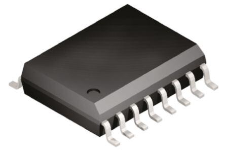
ICGOO电子元器件商城为您提供ADUM6404ARIZ由Analog设计生产,在icgoo商城现货销售,并且可以通过原厂、代理商等渠道进行代购。 ADUM6404ARIZ价格参考。AnalogADUM6404ARIZ封装/规格:数字隔离器, 通用 数字隔离器 5000Vrms 4 通道 1Mbps 25kV/µs CMTI 16-SOIC(0.295",7.50mm 宽)。您可以下载ADUM6404ARIZ参考资料、Datasheet数据手册功能说明书,资料中有ADUM6404ARIZ 详细功能的应用电路图电压和使用方法及教程。
ADUM6404ARIZ 是 Analog Devices Inc. 生产的一款数字隔离器,广泛应用于需要电气隔离和信号传输的场合。其主要应用场景包括:

1. 工业自动化系统:用于PLC(可编程逻辑控制器)、工业I/O模块等设备中,实现控制信号与现场设备之间的电气隔离,提高系统抗干扰能力和安全性。

2. 电源管理系统:适用于隔离式DC-DC转换器、电源监控电路等,实现高压侧与低压侧之间的数据通信和供电一体化。

3. 电机控制与驱动:在变频器、伺服驱动器等设备中,用于隔离控制电路与功率电路,保障控制系统稳定运行。

4. 医疗电子设备:如病人监护仪、医疗成像设备等,满足医用设备对电气安全和患者保护的要求。

5. 通信接口隔离:用于RS-485、CAN总线等工业通信接口中,防止地电位差引起的损坏,提升通信可靠性。

该器件集成了四通道数字隔离功能与片上DC-DC转换器,支持双向通信与独立供电,具备高集成度、高可靠性和简化设计等优点,适用于多种需要信号与电源双重隔离的应用场景。
| 参数 | 数值 |
| 产品目录 | |
| ChannelType | 单向 |
| 描述 | IC DGTL ISO 4CH LOGIC 16SOIC数字隔离器 Quad-CH w/ Intg DC/DC Converter |
| 产品分类 | |
| IsolatedPower | 是 |
| 品牌 | Analog Devices |
| 产品手册 | |
| 产品图片 |
|
| rohs | 符合RoHS无铅 / 符合限制有害物质指令(RoHS)规范要求 |
| 产品系列 | 接口 IC,数字隔离器,Analog Devices ADUM6404ARIZIsoPower®, iCoupler® |
| 数据手册 | |
| 产品型号 | ADUM6404ARIZ |
| PCN设计/规格 | |
| PulseWidthDistortion(Max) | 40ns |
| 上升/下降时间(典型值) | 2.5ns, 2.5ns |
| 产品种类 | |
| 传播延迟 | 100ns |
| 传播延迟tpLH/tpHL(最大值) | 100ns, 100ns |
| 传播延迟时间 | 100 ns |
| 供应商器件封装 | 16-SOIC-IC |
| 共模瞬态抗扰度(最小值) | 25kV/µs |
| 包装 | 管件 |
| 商标 | Analog Devices |
| 安装风格 | SMD/SMT |
| 封装 | Tube |
| 封装/外壳 | 16-SOIC(0.295",7.50mm 宽) |
| 封装/箱体 | SOIC-16 |
| 工作温度 | -40°C ~ 105°C |
| 工厂包装数量 | 37 |
| 技术 | 磁耦合 |
| 数据速率 | 1Mbps |
| 最大工作温度 | + 105 C |
| 最大数据速率 | 1 Mb/s |
| 最小工作温度 | - 40 C |
| 标准包装 | 37 |
| 电压-电源 | 3 V ~ 5.5 V |
| 电压-隔离 | 5000Vrms |
| 电源电压-最大 | 5.5 V |
| 电源电压-最小 | 3 V |
| 电源电流 | 14 mA |
| 类型 | General Purpose |
| 系列 | ADUM6404 |
| 绝缘电压 | 5 kVrms |
| 脉宽失真(最大) | 40ns |
| 视频文件 | http://www.digikey.cn/classic/video.aspx?PlayerID=1364138032001&width=640&height=505&videoID=2219593469001http://www.digikey.cn/classic/video.aspx?PlayerID=1364138032001&width=640&height=505&videoID=2474710092001 |
| 输入-输入侧1/输入侧2 | 0/4 |
| 输出类型 | 逻辑,稳压电压 |
| 通道数 | 4 |
| 通道数量 | 4 Channel |
| 通道类型 | 单向 |
| 隔离式电源 | 是 |


- 商务部:美国ITC正式对集成电路等产品启动337调查
- 曝三星4nm工艺存在良率问题 高通将骁龙8 Gen1或转产台积电
- 太阳诱电将投资9.5亿元在常州建新厂生产MLCC 预计2023年完工
- 英特尔发布欧洲新工厂建设计划 深化IDM 2.0 战略
- 台积电先进制程称霸业界 有大客户加持明年业绩稳了
- 达到5530亿美元!SIA预计今年全球半导体销售额将创下新高
- 英特尔拟将自动驾驶子公司Mobileye上市 估值或超500亿美元
- 三星加码芯片和SET,合并消费电子和移动部门,撤换高东真等 CEO
- 三星电子宣布重大人事变动 还合并消费电子和移动部门
- 海关总署:前11个月进口集成电路产品价值2.52万亿元 增长14.8%


PDF Datasheet 数据手册内容提取
Quad-Channel, 5 kV Isolators with Integrated DC-to-DC Converter Data Sheet ADuM6400/ADuM6401/ADuM6402/ADuM6403/ADuM6404 FEATURES FUNCTIONAL BLOCK DIAGRAMS isoPower integrated, isolated dc-to-dc converter Regulated 5 V or 3.3 V output VDD1 1 OSC RECT REG 16 VISO Up to 400 mW output power GND1 2 15 GNDISO 16-lead SOIC wide body package (RW-16) 16-lead SOIC wide body package with enhanced VIA/VOA 3 4-CHANNELiCOUPLER CORE 14 VIA/VOA creepage (RI-16-1) VIB/VOB 4 ADuM6400/ADuM6401/ 13 VIB/VOB VIC/VOC 5 ADuM6402/ADuM6403/ 12 VIC/VOC Quad dc-to-25 Mbps (NRZ) signal isolation channels ADuM6404 VID/VOD 6 11 VID/VOD Schmitt triggered inputs VDDL 7 10 VSEL HHiigghh tceommpmeorant-umroe doep terraantisoienn: t1 i0m5°mCu mnaitxyi:m >u2m5 k V/μs GND1 8 9 GNDISO 08141-001 Safety and regulatory approvals (RI-16-1 package) Figure 1. UL recognition VIA VOA 5000 V rms for 1 minute per UL 1577 VIB 3 14 VOB 4 13 CSA Component Acceptance Notice #5A (pending) VIC ADuM6400 VOC 5 12 IIEECC 6600690510--11:: 245000 VV rrmmss VID 6 11 VOD 08141-002 VDE certificate of conformity Figure 2. ADuM6400 DIN V VDE V 0884-10 (VDE V 0884-10):2006-12 VIA VOA 3 14 VIORM = 846 V peak VIB VOB 4 13 APPLICATIONS VIC 5 ADuM6401 12 VOC RS-232/RS-422/RS-485 transceivers VOD 6 11 VID 08141-003 Medical isolation Figure 3. ADuM6401 AC/DC power supply start-up bias and gate drives VIA VOA 3 14 Isolated sensor interfaces VIB VOB 4 13 GENERAL DESCRIPTION VOC 5 ADuM6402 12 VIC The ADuM6400/ADuM6401/ADuM6402/ADuM6403/ VOD 6 11 VID 08141-004 ADuM64041 are quad-channel digital isolators with isoPower®, Figure 4. ADuM6402 an integrated, isolated dc-to-dc converter. Based on the Analog VIA VOA 3 14 Devices, Inc., iCoupler® technology, the dc-to-dc converter provides VOB VIB 4 13 up to 400 mW of regulated, isolated power at either 5.0 V or 3.3 V VOC ADuM6403 VIC 5 12 fproowme ra l5e.v0e lVs sinhpowutn s uinp pTlayb, loer 1 a. tT 3h.3e sVe dfreovmic eas 3e.l3im Vi nsuatpep tlhy ea tn teheed VOD 6 11 VID 08141-005 Figure 5. ADuM6403 for a separate, isolated dc-to-dc converter in low power, isolated designs. VOA VIA 3 14 VOB VIB The ADuM6400/ADuM6401/ADuM6402/ADuM6403/ 4 13 VOC ADuM6404 VIC ADuM6404 isolators provide four independent isolation 5 12 channels in a variety of channel configurations and data rates VOD 6 11 VID 08141-006 (see the Ordering Guide for more information). Figure 6. ADuM6404 Table 1. Power Levels isoPower uses high frequency switching elements to transfer power Input Voltage Output Voltage Output Power through its transformer. Special care must be taken during printed circuit board (PCB) layout to meet emissions standards. See the 5.0 V 5.0 V 400 mW AN-0971 Application Note for board layout recommendations. 5.0 V 3.3 V 330 mW 3.3 V 3.3 V 132 mW 1 Protected by U.S. Patents 5,952,849; 6,873,065; 6,903,578; and 7,075,329. Rev. A Information furnished by Analog Devices is believed to be accurate and reliable. However, no responsibility is assumed by Analog Devices for its use, nor for any infringements of patents or other One Technology Way, P.O. Box 9106, Norwood, MA 02062-9106, U.S.A. rights of third parties that may result from its use. Specifications subject to change without notice. No license is granted by implication or otherwise under any patent or patent rights of Analog Devices. Tel: 781.329.4700 www.analog.com Trademarks and registered trademarks are the property of their respective owners. Fax: 781.461.3113 ©2009–2012 Analog Devices, Inc. All rights reserved.
ADuM6400/ADuM6401/ADuM6402/ADuM6403/ADuM6404 Data Sheet TABLE OF CONTENTS Features .............................................................................................. 1 Pin Configurations and Function Descriptions ......................... 12 Applications ....................................................................................... 1 Truth Table .................................................................................. 16 General Description ......................................................................... 1 Typical Performance Characteristics ........................................... 17 Functional Block Diagrams ............................................................. 1 Terminology .................................................................................... 20 Revision History ............................................................................... 2 Applications Information .............................................................. 21 Specifications ..................................................................................... 3 PCB Layout ................................................................................. 21 Electrical Characteristics—5 V Primary Input Supply/ Start-Up Behavior....................................................................... 21 5 V Secondary Isolated Supply ................................................... 3 EMI Considerations ................................................................... 22 Electrical Characteristics—3.3 V Primary Input Supply/ Propagation Delay Parameters ................................................. 22 3.3 V Secondary Isolated Supply ................................................ 5 DC Correctness and Magnetic Field Immunity ..................... 22 Electrical Characteristics—5 V Primary Input Supply/ 3.3 V Secondary Isolated Supply ................................................ 6 Power Consumption .................................................................. 23 Package Characteristics ............................................................... 8 Current Limit and Thermal Overload Protection ................. 24 Regulatory Information ............................................................... 9 Power Considerations ................................................................ 24 Insulation and Safety-Related Specifications ............................ 9 Thermal Analysis ....................................................................... 25 Insulation Characteristics .......................................................... 10 Insulation Lifetime ..................................................................... 25 Recommended Operating Conditions .................................... 10 Outline Dimensions ....................................................................... 26 Absolute Maximum Ratings .......................................................... 11 Ordering Guide .......................................................................... 27 ESD Caution ................................................................................ 11 REVISION HISTORY 4/12—Rev. 0 to Rev. A Changes to Figure 19 and Figure 20............................................. 18 Changes to Features Section, General Description Section, Added Figure 21 and Figure 22; Renumbered and Table 1 ......................................................................................... 1 Figures Sequentially ....................................................................... 18 Changes to Table 2 and Table 3 ....................................................... 3 Added Definition of I to Terminology Section .............. 20 ISO(LOAD) Changes to Endnote 1 in Table 5 .................................................... 4 Changes to PCB Layout Section ................................................... 21 Changes to Table 6 and Table 7 ....................................................... 5 Added Start-Up Behavior Section ................................................ 21 Change to Propagation Delay Parameter in Table 8 .................... 5 Changes to EMI Considerations Section .................................... 22 Changes to Endnote 1 in Table 9; Changes to Table 10 ............... 6 Moved Propagation Delay Parameters Section .......................... 22 Changes to Table 11 .......................................................................... 7 Changes to Power Consumption Section .................................... 23 Changes to Endnote 1 in Table 13; Changes to Table 14 ............. 8 Added Current Limit and Thermal Overload Protection Changes to Regulatory Information Section, Table 15, Section .............................................................................................. 24 and Table 16 ....................................................................................... 9 Moved Thermal Analysis Section ................................................ 25 Changes to Insulation Characteristics Section, Table 17, Changes to Insulation Lifetime Section and Figure 33 ............. 25 and Table 18 ..................................................................................... 10 Updated Outline Dimensions ....................................................... 26 Changes to Table 20 ........................................................................ 11 Changes to Ordering Guide .......................................................... 27 Changes to Table 26 ........................................................................ 16 Changes to Figure 13, Figure 14, Figure 15, Figure 17, 5/09—Revision 0: Initial Version and Figure 18 ................................................................................... 17 Rev. A | Page 2 of 28
Data Sheet ADuM6400/ADuM6401/ADuM6402/ADuM6403/ADuM6404 SPECIFICATIONS ELECTRICAL CHARACTERISTICS—5 V PRIMARY INPUT SUPPLY/5 V SECONDARY ISOLATED SUPPLY Typical specifications are at T = 25°C, V = V = V = 5 V. Minimum/maximum specifications apply over the entire recommended A DD1 SEL ISO operation range, which is 4.5 V ≤ V , V , V ≤ 5.5 V, and −40°C ≤ T ≤ +105°C, unless otherwise noted. Switching specifications are DD1 SEL ISO A tested with C = 15 pF and CMOS signal levels, unless otherwise noted. L Table 2. DC-to-DC Converter Static Specifications Parameter Symbol Min Typ Max Unit Test Conditions/Comments DC-TO-DC CONVERTER SUPPLY Setpoint V 4.7 5.0 5.4 V I = 0 mA ISO ISO Line Regulation V 1 mV/V I = 40 mA, V = 4.5 V to 5.5 V ISO(LINE) ISO DD1 Load Regulation V 1 5 % I = 8 mA to 72 mA ISO(LOAD) ISO Output Ripple V 75 mV p-p 20 MHz bandwidth, C = 0.1 μF||10 μF, I = 72 mA ISO(RIP) BO ISO Output Noise V 200 mV p-p C = 0.1 μF||10 μF, I = 72 mA ISO(NOISE) BO ISO Switching Frequency f 180 MHz OSC PWM Frequency f 625 kHz PWM Output Supply Current I 80 mA V > 4.5 V ISO(MAX) ISO Efficiency at I 34 % I = 80 mA ISO(MAX) ISO I , No V Load I 13 35 mA DD1 ISO DD1(Q) I , Full V Load I 290 mA DD1 ISO DD1(MAX) Table 3. DC-to-DC Converter Dynamic Specifications 1 Mbps—A or C Grade 25 Mbps—C Grade Test Conditions/ Parameter Symbol Min Typ Max Min Typ Max Unit Comments SUPPLY CURRENT Input I DD1(D) ADuM6400 12 64 mA No V load ISO ADuM6401 12 68 mA No V load ISO ADuM6402 13 71 mA No V load ISO ADuM6403 14 75 mA No V load ISO ADuM6404 14 78 mA No V load ISO Available to Load I ISO(LOAD) ADuM6400 80 69 mA ADuM6401 80 67 mA ADuM6402 80 65 mA ADuM6403 80 63 mA ADuM6404 80 61 mA Rev. A | Page 3 of 28
ADuM6400/ADuM6401/ADuM6402/ADuM6403/ADuM6404 Data Sheet Table 4. Switching Specifications A Grade C Grade Test Conditions/ Parameter Symbol Min Typ Max Min Typ Max Unit Comments SWITCHING SPECIFICATIONS Data Rate 1 25 Mbps Within PWD limit Propagation Delay t , t 55 100 45 60 ns 50% input to 50% output PHL PLH Pulse Width Distortion PWD 40 6 ns |t − t | PLH PHL Change vs. Temperature 5 ps/°C Pulse Width PW 1000 40 ns Within PWD limit Propagation Delay Skew t 50 15 ns Between any two units PSK Channel Matching Codirectional1 t 50 6 ns PSKCD Opposing Directional2 t 50 15 ns PSKOD 1 Codirectional channel matching is the absolute value of the difference in propagation delays between any two channels with inputs on the same side of the isolation 7 barrier. 2 Opposing directional channel matching is the absolute value of the difference in propagation delays between any two channels with inputs on opposite sides of the isolation barrier. Table 5. Input and Output Characteristics Test Conditions/ Parameter Symbol Min Typ Max Unit Comments DC SPECIFICATIONS Logic High Input Threshold V 0.7 × V or 0.7 × V V IH ISO DD1 Logic Low Input Threshold V 0.3 × V or 0.3 × V V IL ISO DD1 Logic High Output Voltages V V − 0.3 or V − 0.3 5.0 V I = −20 μA, V = V OH DD1 ISO Ox Ix IxH V − 0.5 or V − 0.5 4.8 V I = −4 mA, V = V DD1 ISO Ox Ix IxH Logic Low Output Voltages V 0.0 0.1 V I = 20 μA, V = V OL Ox Ix IxL 0.2 0.4 V I = 4 mA, V = V Ox Ix IxL Undervoltage Lockout UVLO V , V , V supplies DD1 DDL ISO Positive-Going Threshold V 2.7 V UV+ Negative-Going Threshold V 2.4 V UV− Hysteresis V 0.3 V UVH Input Currents per Channel I −20 +0.01 +20 μA 0 V ≤ V ≤ V I Ix DDx AC SPECIFICATIONS Output Rise/Fall Time t/t 2.5 ns 10% to 90% R F Common-Mode Transient |CM| 25 35 kV/μs V = V or V , V = 1000 V, Ix DD1 ISO CM Immunity1 transient magnitude = 800 V Refresh Rate f 1.0 Mbps r 1 |CM| is the maximum common-mode voltage slew rate that can be sustained while maintaining VO > 0.7 × VDD1 or 0.7 × VISO for a high input or VO < 0.3 × VDD1 or 0.3 × VISO for a low input. The common-mode voltage slew rates apply to both rising and falling common-mode voltage edges. Rev. A | Page 4 of 28
Data Sheet ADuM6400/ADuM6401/ADuM6402/ADuM6403/ADuM6404 ELECTRICAL CHARACTERISTICS—3.3 V PRIMARY INPUT SUPPLY/3.3 V SECONDARY ISOLATED SUPPLY Typical specifications are at T = 25°C, V = V = 3.3 V, V = GND . Minimum/maximum specifications apply over the entire A DD1 ISO SEL ISO recommended operation range, which is 3.0 V ≤ V , V , V ≤ 3.6 V, and −40°C ≤ T ≤ +105°C, unless otherwise noted. Switching DD1 SEL ISO A specifications are tested with C = 15 pF and CMOS signal levels, unless otherwise noted. L Table 6. DC-to-DC Converter Static Specifications Parameter Symbol Min Typ Max Unit Test Conditions/Comments DC-TO-DC CONVERTER SUPPLY Setpoint V 3.0 3.3 3.6 V I = 0 mA ISO ISO Line Regulation V 1 mV/V I = 20 mA, V = 3.0 V to 3.6 V ISO(LINE) ISO DD1 Load Regulation V 1 5 % I = 4 mA to 36 mA ISO(LOAD) ISO Output Ripple V 50 mV p-p 20 MHz bandwidth, C = 0.1 μF||10 μF, I = 54 mA ISO(RIP) BO ISO Output Noise V 130 mV p-p C = 0.1 μF||10 μF, I = 54 mA ISO(NOISE) BO ISO Switching Frequency f 180 MHz OSC PWM Frequency f 625 kHz PWM Output Supply Current I 40 mA V > 3 V ISO(MAX) ISO Efficiency at I 33 % I = 40 mA ISO(MAX) ISO I , No V Load I 15 28 mA DD1 ISO DD1(Q) I , Full V Load I 175 mA DD1 ISO DD1(MAX) Table 7. DC-to-DC Converter Dynamic Specifications 1 Mbps—A or C Grade 25 Mbps—C Grade Test Conditions/ Parameter Symbol Min Typ Max Min Typ Max Unit Comments SUPPLY CURRENT Input I DD1(D) ADuM6400 8 41 mA No V load ISO ADuM6401 8 44 mA No V load ISO ADuM6402 8 46 mA No V load ISO ADuM6403 9 47 mA No V load ISO ADuM6404 9 51 mA No V load ISO Available to Load I ISO(LOAD) ADuM6400 40 33 mA ADuM6401 40 31 mA ADuM6402 40 30 mA ADuM6403 40 29 mA ADuM6404 40 28 mA Table 8. Switching Specifications A Grade C Grade Test Conditions/ Parameter Symbol Min Typ Max Min Typ Max Unit Comments SWITCHING SPECIFICATIONS Data Rate 1 25 Mbps Within PWD limit Propagation Delay t , t 60 100 45 65 ns 50% input to 50% output PHL PLH Pulse Width Distortion PWD 40 6 ns |t − t | PLH PHL Change vs. Temperature 5 ps/°C Pulse Width PW 1000 40 ns Within PWD limit Propagation Delay Skew t 50 45 ns Between any two units PSK Channel Matching Codirectional1 t 50 6 ns PSKCD Opposing Directional2 t 50 15 ns PSKOD 1 Codirectional channel matching is the absolute value of the difference in propagation delays between any two channels with inputs on the same side of the isolation 7 barrier. 2 Opposing directional channel matching is the absolute value of the difference in propagation delays between any two channels with inputs on opposite sides of the isolation barrier. Rev. A | Page 5 of 28
ADuM6400/ADuM6401/ADuM6402/ADuM6403/ADuM6404 Data Sheet Table 9. Input and Output Characteristics Test Conditions/ Parameter Symbol Min Typ Max Unit Comments DC SPECIFICATIONS Logic High Input Threshold V 0.7 × V or 0.7 × V V IH ISO DD1 Logic Low Input Threshold V 0.3 × V or 0.3 × V V IL ISO DD1 Logic High Output Voltages V V − 0.2 or V − 0.2 3.3 V I = −20 μA, V = V OH DD1 ISO Ox Ix IxH V − 0.5 or V − 0.5 3.1 V I = −4 mA, V = V DD1 ISO Ox Ix IxH Logic Low Output Voltages V 0.0 0.1 V I = 20 μA, V = V OL Ox Ix IxL 0.0 0.4 V I = 4 mA, V = V Ox Ix IxL Undervoltage Lockout UVLO V , V , V supplies DD1 DDL ISO Positive-Going Threshold V 2.7 V UV+ Negative-Going Threshold V 2.4 V UV− Hysteresis V 0.3 V UVH Input Currents per Channel I −10 +0.01 +10 μA 0 V ≤ V ≤ V I Ix DDx AC SPECIFICATIONS Output Rise/Fall Time t/t 2.5 ns 10% to 90% R F Common-Mode Transient |CM| 25 35 kV/μs V = V or V , V = 1000 V, Ix DD1 ISO CM Immunity1 transient magnitude = 800 V Refresh Rate f 1.0 Mbps r 1 |CM| is the maximum common-mode voltage slew rate that can be sustained while maintaining VO > 0.7 × VDD1 or 0.7 × VISO for a high input or VO < 0.3 × VDD1 or 0.3 × VISO for a low input. The common-mode voltage slew rates apply to both rising and falling common-mode voltage edges. ELECTRICAL CHARACTERISTICS—5 V PRIMARY INPUT SUPPLY/3.3 V SECONDARY ISOLATED SUPPLY Typical specifications are at T = 25°C, V = 5.0 V, V = 3.3 V, V = GND . Minimum/maximum specifications apply over the entire A DD1 ISO SEL ISO recommended operation range, which is 4.5 V ≤ V ≤ 5.5 V, 3.0 V ≤ V ≤ 3.6 V, and −40°C ≤ T ≤ +105°C, unless otherwise noted. DD1 ISO A Switching specifications are tested with C = 15 pF and CMOS signal levels, unless otherwise noted. L Table 10. DC-to-DC Converter Static Specifications Parameter Symbol Min Typ Max Unit Test Conditions/Comments DC-TO-DC CONVERTER SUPPLY Setpoint V 3.0 3.3 3.6 V I = 0 mA ISO ISO Line Regulation V 1 mV/V I = 50 mA, V = 4.5 V to 5.5 V ISO(LINE) ISO DD1 Load Regulation V 1 5 % I = 10 mA to 90 mA ISO(LOAD) ISO Output Ripple V 50 mV p-p 20 MHz bandwidth, C = 0.1 μF||10 μF, I = 90 mA ISO(RIP) BO ISO Output Noise V 130 mV p-p C = 0.1 μF||10 μF, I = 90 mA ISO(NOISE) BO ISO Switching Frequency f 180 MHz OSC PWM Frequency f 625 kHz PWM Output Supply Current I 100 mA V > 3 V ISO(MAX) ISO Efficiency at I 30 % I = 100 mA ISO(MAX) ISO I , No V Load I 11 20 mA DD1 ISO DD1(Q) I , Full V Load I 230 mA DD1 ISO DD1(MAX) Rev. A | Page 6 of 28
Data Sheet ADuM6400/ADuM6401/ADuM6402/ADuM6403/ADuM6404 Table 11. DC-to-DC Converter Dynamic Specifications 1 Mbps—A or C Grade 25 Mbps—C Grade Test Conditions/ Parameter Symbol Min Typ Max Min Typ Max Unit Comments SUPPLY CURRENT Input I DD1(D) ADuM6400 6 43 mA No V load ISO ADuM6401 6 44 mA No V load ISO ADuM6402 7 45 mA No V load ISO ADuM6403 7 46 mA No V load ISO ADuM6404 7 47 mA No V load ISO Available to Load I ISO(LOAD) ADuM6400 100 93 mA ADuM6401 100 92 mA ADuM6402 100 91 mA ADuM6403 100 89 mA ADuM6404 100 88 mA Table 12. Switching Specifications A Grade C Grade Test Conditions/ Parameter Symbol Min Typ Max Min Typ Max Unit Comments SWITCHING SPECIFICATIONS Data Rate 1 25 Mbps Within PWD limit Propagation Delay t , t 60 100 45 60 ns 50% input to 50% output PHL PLH Pulse Width Distortion PWD 40 6 ns |t − t | PLH PHL Change vs. Temperature 5 ps/°C Pulse Width PW 1000 40 ns Within PWD limit Propagation Delay Skew t 50 15 ns Between any two units PSK Channel Matching Codirectional1 t 50 6 ns PSKCD Opposing Directional2 t 50 15 ns PSKOD 1 Codirectional channel matching is the absolute value of the difference in propagation delays between any two channels with inputs on the same side of the isolation 7 barrier. 2 Opposing directional channel matching is the absolute value of the difference in propagation delays between any two channels with inputs on opposite sides of the isolation barrier. Rev. A | Page 7 of 28
ADuM6400/ADuM6401/ADuM6402/ADuM6403/ADuM6404 Data Sheet Table 13. Input and Output Characteristics Parameter Symbol Min Typ Max Unit Test Conditions/Comments DC SPECIFICATIONS Logic High Input Threshold V 0.7 × V or V IH ISO 0.7 × V DD1 Logic Low Input Threshold V 0.3 × V or V IL ISO 0.3 × V DD1 Logic High Output Voltages V V − 0.2 or V or V V I = −20 μA, V = V OH DD1 DD1 ISO Ox Ix IxH V − 0.2 ISO V − 0.5 or V − 0.2 or V I = −4 mA, V = V DD1 DD1 Ox Ix IxH V − 0.5 V − 0.2 ISO ISO Logic Low Output Voltages V 0.0 0.1 V I = 20 μA, V = V OL Ox Ix IxL 0.0 0.4 V I = 4 mA, V = V Ox Ix IxL Undervoltage Lockout UVLO V , V , V supplies DD1 DDL ISO Positive-Going Threshold V 2.7 V UV+ Negative-Going Threshold V 2.4 V UV− Hysteresis V 0.3 V UVH Input Currents per Channel I −10 +0.01 +10 μA 0 V ≤ V ≤ V I Ix DDx AC SPECIFICATIONS Output Rise/Fall Time t/t 2.5 ns 10% to 90% R F Common-Mode Transient |CM| 25 35 kV/μs V = V or V , V = 1000 V, Ix DD1 ISO CM Immunity1 transient magnitude = 800 V Refresh Rate f 1.0 Mbps r 1 |CM| is the maximum common-mode voltage slew rate that can be sustained while maintaining VO > 0.7 × VDD1 or 0.7 × VISO for a high input or VO < 0.3 × VDD1 or 0.3 × VISO for a low input. The common-mode voltage slew rates apply to both rising and falling common-mode voltage edges. PACKAGE CHARACTERISTICS Table 14. Parameter Symbol Min Typ Max Unit Test Conditions/Comments RESISTANCE AND CAPACITANCE Resistance (Input-to-Output)1 R 1012 Ω I-O Capacitance (Input-to-Output)1 C 2.2 pF f = 1 MHz I-O Input Capacitance2 C 4.0 pF I IC Junction-to-Ambient Thermal θ 45 °C/W Thermocouple is located at the center of JA Resistance the package underside; test conducted on a 4-layer board with thin traces3 THERMAL SHUTDOWN Thermal Shutdown Threshold TS 150 °C T rising SD J Thermal Shutdown Hysteresis TS 20 °C SD-HYS 1 This device is considered a 2-terminal device; Pin 1 through Pin 8 are shorted together, and Pin 9 through Pin 16 are shorted together. 2 Input capacitance is from any input data pin to ground. 3 Refer to the Thermal Analysis section for thermal model definitions. Rev. A | Page 8 of 28
Data Sheet ADuM6400/ADuM6401/ADuM6402/ADuM6403/ADuM6404 REGULATORY INFORMATION The ADuM6400/ADuM6401/ADuM6402/ADuM6403/ADuM6404 are approved by the organizations listed in Table 15. Refer to Table 20 and the Insulation Lifetime section for more information about the recommended maximum working voltages for specific cross-insulation waveforms and insulation levels. Table 15. UL1 CSA (Pending) VDE Recognized under UL 1577 component Approved under CSA Component Acceptance Notice #5A RW-16 package:2 recognition program Certified according to IEC 60747-5-2 (VDE 0884 Part 2):2003-01 (pending) Basic insulation, 846 V peak Single protection, 5000 V rms isolation Basic insulation per CSA 60950-1-07 and IEC 60950-1, RI-16-1 package:3 voltage 600 V rms (848 V peak) maximum working voltage Certified according to DIN V VDE V 0884-10 (VDE V 0884-10):2006-12 Reinforced insulation, 846 V peak RW-16 package: Reinforced insulation per CSA 60950-1-07 and IEC 60950-1, 380 V rms (537 V peak) maximum working voltage Reinforced insulation per IEC 60601-1, 125 V rms (176 V peak) maximum working voltage RI-16-1 package: Reinforced insulation per CSA 60950-1-07 and IEC 60950-1, 400 V rms (565 V peak) maximum working voltage Reinforced insulation per IEC 60601-1, 250 V rms (353 V peak) maximum working voltage File E214100 File 205078 File 2471900-4880-0001 1 In accordance with UL 1577, each ADuM6400/ADuM6401/ADuM6402/ADuM6403/ADuM6404 is proof-tested by applying an insulation test voltage ≥ 6000 V rms for 1 sec (current leakage detection limit = 20 μA). 2 In accordance with IEC 60747-5-2 (VDE 0884 Part 2):2003-01, each ADuM6400/ADuM6401/ADuM6402/ADuM6403/ADuM6404 in the RW-16 package is proof-tested by applying an insulation test voltage ≥ 1590 V peak for 1 sec (partial discharge detection limit = 5 pC). The asterisk (*) marking branded on the component designates IEC 60747-5-2 (VDE 0884 Part 2):2003-01 approval. 3 In accordance with DIN V VDE V 0884-10 (VDE V 0884-10):2006-12, each ADuM6400/ADuM6401/ADuM6402/ADuM6403/ADuM6404 in the RI-16-1 package is proof-tested by applying an insulation test voltage ≥ 1590 V peak for 1 sec (partial discharge detection limit = 5 pC). The asterisk (*) marking branded on the component designates DIN V VDE V 0884-10 (VDE V 0884-10):2006-12 approval. INSULATION AND SAFETY-RELATED SPECIFICATIONS Table 16. Parameter Symbol Value Unit Test Conditions/Comments Rated Dielectric Insulation Voltage 5000 V rms 1-minute duration Minimum External Air Gap (Clearance) L(I01) 8.0 mm Measured from input terminals to output terminals, shortest distance through air Minimum External Tracking (Creepage) L(I02) Measured from input terminals to output terminals, shortest distance path along body RW-16 Package 7.6 mm RI-16-1 Package 8.3 mm Minimum Internal Distance (Internal Clearance) 0.017 min mm Distance through insulation Tracking Resistance (Comparative Tracking Index) CTI >175 V DIN IEC 112/VDE 0303, Part 1 Material Group IIIa Material Group (DIN VDE 0110, 1/89, Table 1) Rev. A | Page 9 of 28
ADuM6400/ADuM6401/ADuM6402/ADuM6403/ADuM6404 Data Sheet INSULATION CHARACTERISTICS IEC 60747-5-2 (VDE 0884 Part 2):2003-01 and DIN V VDE V 0884-10 (VDE V 0884-10):2006-12 These isolators are suitable for reinforced electrical isolation only within the safety limit data. Maintenance of the safety data is ensured by protective circuits. The asterisk (*) marking branded on the components designates IEC 60747-5-2 (VDE 0884 Part 2):2003-01 or DIN V VDE V 0884-10 (VDE V 0884-10):2006-12 approval. Table 17. Description Test Conditions/Comments Symbol Characteristic Unit Installation Classification per DIN VDE 0110 For Rated Mains Voltage ≤ 300 V rms I to IV For Rated Mains Voltage ≤ 450 V rms I to II For Rated Mains Voltage ≤ 600 V rms I to II Climatic Classification 40/105/21 Pollution Degree per DIN VDE 0110, Table 1 2 Maximum Working Insulation Voltage V 846 V peak IORM Input-to-Output Test Voltage Method b1 V × 1.875 = V , 100% production test, t = 1 sec, V 1590 V peak IORM PR m PR partial discharge < 5 pC Method a V PR After Environmental Tests Subgroup 1 V × 1.6 = V , t = 60 sec, partial discharge < 5 pC 1375 V peak IORM PR m After Input and/or Safety Tests V × 1.2 = V , t = 60 sec, partial discharge < 5 pC 1018 V peak IORM PR m Subgroup 2 and Subgroup 3 Highest Allowable Overvoltage Transient overvoltage, t = 10 sec V 6000 V peak TR IOTM Safety-Limiting Values Maximum value allowed in the event of a failure (see Figure 7) Case Temperature T 150 °C S Side 1 Current (I ) I 555 mA DD1 S1 Insulation Resistance at T V = 500 V R >109 Ω S IO S Thermal Derating Curve 600 A) m500 T ( N E R R400 U C D1 VD300 G N TI RA200 E P O FE 100 A S 00 50AMBIENT TEM10P0ERATURE (°C1)50 200 08141-007 Figure 7. Thermal Derating Curve, Dependence of Safety-Limiting Values on Case Temperature, per DIN EN 60747-5-2 RECOMMENDED OPERATING CONDITIONS Table 18. Parameter Symbol Min Max Unit Test Conditions/Comments TEMPERATURE Operating Temperature T −40 +105 °C Operation at 105°C requires reduction of the A maximum load current as specified in Table 19 SUPPLY VOLTAGES V Each voltage is relative to its respective ground DD1 V @ V = GND 3.0 5.5 V DD1 SEL ISO V @ V = V 4.5 5.5 V DD1 SEL ISO Rev. A | Page 10 of 28
Data Sheet ADuM6400/ADuM6401/ADuM6402/ADuM6403/ADuM6404 ABSOLUTE MAXIMUM RATINGS T = 25°C, unless otherwise noted. Stresses above those listed under Absolute Maximum Ratings A may cause permanent damage to the device. This is a stress Table 19. rating only; functional operation of the device at these or any Parameter Rating other conditions above those indicated in the operational Storage Temperature Range (TST) −55°C to +150°C section of this specification is not implied. Exposure to absolute Ambient Operating Temperature −40°C to +105°C maximum rating conditions for extended periods may affect Range (T ) A device reliability. Supply Voltages (V , V , V )1 −0.5 V to +7.0 V DD1 DDL ISO Input Voltage (V , V , V , V , V )1, 2 −0.5 V to V + 0.5 V IA IB IC ID SEL DDI Output Voltage (V , V , V , V )1, 2 −0.5 V to V + 0.5 V ESD CAUTION OA OB OC OD DDO Average Output Current per Pin3 −10 mA to +10 mA Common-Mode Transients4 −100 kV/μs to +100 kV/μs 1 Each voltage is relative to its respective ground. 2 VDDI and VDDO refer to the supply voltages on the input and output sides of a given channel, respectively. See the PCB Layout section. 3 See Figure 7 for maximum rated current values for various temperatures. 4 Common-mode transients exceeding the absolute maximum ratings may cause latch-up or permanent damage. Table 20. Maximum Continuous Working Voltage1 Parameter Max Unit Applicable Certification AC Voltage, Bipolar Waveform 424 V peak All certifications, 50-year operation AC Voltage, Unipolar Waveform Basic Insulation 600 V peak Reinforced Insulation 565 V peak Working voltage per IEC 60950-1 DC Voltage Basic Insulation 600 V peak Reinforced Insulation 565 V peak Working voltage per IEC 60950-1 1 Refers to the continuous voltage magnitude imposed across the isolation barrier. See the Insulation Lifetime section for more information. Rev. A | Page 11 of 28
ADuM6400/ADuM6401/ADuM6402/ADuM6403/ADuM6404 Data Sheet PIN CONFIGURATIONS AND FUNCTION DESCRIPTIONS VDD1 1 16 VISO GND1 2 15 GNDISO VIA 3 ADuM6400 14 VOA VIB 4 TOP VIEW 13 VOB VIC 5 (Not to Scale) 12 VOC VID 6 11 VOD GVNDDDL1 87 190 VGSNEDLISO 08141-008 Figure 8. ADuM6400 Pin Configuration Table 21. ADuM6400 Pin Function Descriptions Pin No. Mnemonic Description 1 V Primary Supply Voltage, 3.0 V to 5.5 V. Pin 1 and Pin 7 must be connected to the same external voltage source. DD1 2, 8 GND Ground Reference for the Primary Side of the Isolator. Pin 2 and Pin 8 are internally connected to each other, and 1 it is recommended that both pins be connected to a common ground. 3 V Logic Input A. IA 4 V Logic Input B. IB 5 V Logic Input C. IC 6 V Logic Input D. ID 7 V Data Channel Supply Voltage, 3.0 V to 5.5 V. Pin 1 and Pin 7 must be connected to the same external voltage source. DDL 9, 15 GND Ground Reference for the Secondary Side of the Isolator. Pin 9 and Pin 15 are internally connected to each other, ISO and it is recommended that both pins be connected to a common ground. 10 V Output Voltage Selection. When V = V , the V setpoint is 5.0 V. When V = GND , the V setpoint is 3.3 V. SEL SEL ISO ISO SEL ISO ISO 11 V Logic Output D. OD 12 V Logic Output C. OC 13 V Logic Output B. OB 14 V Logic Output A. OA 16 V Secondary Supply Voltage Output for External Loads: 3.3 V (V = GND ) or 5.0 V (V = V ). ISO SEL ISO SEL ISO Rev. A | Page 12 of 28
Data Sheet ADuM6400/ADuM6401/ADuM6402/ADuM6403/ADuM6404 VDD1 1 16 VISO GND1 2 15 GNDISO VIA 3 ADuM6401 14 VOA VIB 4 TOP VIEW 13 VOB VIC 5 (Not to Scale) 12 VOC VOD 6 11 VID GVNDDDL1 87 190 VGSNEDLISO 08141-009 Figure 9. ADuM6401 Pin Configuration Table 22. ADuM6401 Pin Function Descriptions Pin No. Mnemonic Description 1 V Primary Supply Voltage, 3.0 V to 5.5 V. Pin 1 and Pin 7 must be connected to the same external voltage source. DD1 2, 8 GND Ground Reference for the Primary Side of the Isolator. Pin 2 and Pin 8 are internally connected to each other, and 1 it is recommended that both pins be connected to a common ground. 3 V Logic Input A. IA 4 V Logic Input B. IB 5 V Logic Input C. IC 6 V Logic Output D. OD 7 V Data Channel Supply Voltage, 3.0 V to 5.5 V. Pin 1 and Pin 7 must be connected to the same external voltage source. DDL 9, 15 GND Ground Reference for the Secondary Side of the Isolator. Pin 9 and Pin 15 are internally connected to each other, ISO and it is recommended that both pins be connected to a common ground. 10 V Output Voltage Selection. When V = V , the V setpoint is 5.0 V. When V = GND , the V setpoint is 3.3 V. SEL SEL ISO ISO SEL ISO ISO 11 V Logic Input D. ID 12 V Logic Output C. OC 13 V Logic Output B. OB 14 V Logic Output A. OA 16 V Secondary Supply Voltage Output for External Loads: 3.3 V (V = GND ) or 5.0 V (V = V ). ISO SEL ISO SEL ISO Rev. A | Page 13 of 28
ADuM6400/ADuM6401/ADuM6402/ADuM6403/ADuM6404 Data Sheet VDD1 1 16 VISO GND1 2 15 GNDISO VIA 3 ADuM6402 14 VOA VIB 4 TOP VIEW 13 VOB VOC 5 (Not to Scale) 12 VIC VOD 6 11 VID GVNDDDL1 87 190 VGSNEDLISO 08141-010 Figure 10. ADuM6402 Pin Configuration Table 23. ADuM6402 Pin Function Descriptions Pin No. Mnemonic Description 1 V Primary Supply Voltage, 3.0 V to 5.5 V. Pin 1 and Pin 7 must be connected to the same external voltage source. DD1 2, 8 GND Ground Reference for the Primary Side of the Isolator. Pin 2 and Pin 8 are internally connected to each other, and 1 it is recommended that both pins be connected to a common ground. 3 V Logic Input A. IA 4 V Logic Input B. IB 5 V Logic Output C. OC 6 V Logic Output D. OD 7 V Data Channel Supply Voltage, 3.0 V to 5.5 V. Pin 1 and Pin 7 must be connected to the same external voltage source. DDL 9, 15 GND Ground Reference for the Secondary Side of the Isolator. Pin 9 and Pin 15 are internally connected to each other, ISO and it is recommended that both pins be connected to a common ground. 10 V Output Voltage Selection. When V = V , the V setpoint is 5.0 V. When V = GND , the V setpoint is 3.3 V. SEL SEL ISO ISO SEL ISO ISO 11 V Logic Input D. ID 12 V Logic Input C. IC 13 V Logic Output B. OB 14 V Logic Output A. OA 16 V Secondary Supply Voltage Output for External Loads: 3.3 V (V = GND ) or 5.0 V (V = V ). ISO SEL ISO SEL ISO Rev. A | Page 14 of 28
Data Sheet ADuM6400/ADuM6401/ADuM6402/ADuM6403/ADuM6404 VDD1 1 16 VISO GND1 2 15 GNDISO VIA 3 ADuM6403 14 VOA VOB 4 TOP VIEW 13 VIB VOC 5 (Not to Scale) 12 VIC VOD 6 11 VID GVNDDDL1 87 190 VGSNEDLISO 08141-011 Figure 11. ADuM6403 Pin Configuration Table 24. ADuM6403 Pin Function Descriptions Pin No. Mnemonic Description 1 V Primary Supply Voltage, 3.0 V to 5.5 V. Pin 1 and Pin 7 must be connected to the same external voltage source. DD1 2, 8 GND Ground Reference for the Primary Side of the Isolator. Pin 2 and Pin 8 are internally connected to each other, and 1 it is recommended that both pins be connected to a common ground. 3 V Logic Input A. IA 4 V Logic Output B. OB 5 V Logic Output C. OC 6 V Logic Output D. OD 7 V Data Channel Supply Voltage, 3.0 V to 5.5 V. Pin 1 and Pin 7 must be connected to the same external voltage source. DDL 9, 15 GND Ground Reference for the Secondary Side of the Isolator. Pin 9 and Pin 15 are internally connected to each other, ISO and it is recommended that both pins be connected to a common ground. 10 V Output Voltage Selection. When V = V , the V setpoint is 5.0 V. When V = GND , the V setpoint is 3.3 V. SEL SEL ISO ISO SEL ISO ISO 11 V Logic Input D. ID 12 V Logic Input C. IC 13 V Logic Input B. IB 14 V Logic Output A. OA 16 V Secondary Supply Voltage Output for External Loads: 3.3 V (V = GND ) or 5.0 V (V = V ). ISO SEL ISO SEL ISO Rev. A | Page 15 of 28
ADuM6400/ADuM6401/ADuM6402/ADuM6403/ADuM6404 Data Sheet VDD1 1 16 VISO GND1 2 15 GNDISO VOA 3 ADuM6404 14 VIA VOB 4 TOP VIEW 13 VIB VOC 5 (Not to Scale) 12 VIC VOD 6 11 VID GVNDDDL1 87 190 VGSNEDLISO 08141-012 Figure 12. ADuM6404 Pin Configuration Table 25. ADuM6404 Pin Function Descriptions Pin No. Mnemonic Description 1 V Primary Supply Voltage, 3.0 V to 5.5 V. Pin 1 and Pin 7 must be connected to the same external voltage source. DD1 2, 8 GND Ground Reference for the Primary Side of the Isolator. Pin 2 and Pin 8 are internally connected to each other, and 1 it is recommended that both pins be connected to a common ground. 3 V Logic Output A. OA 4 V Logic Output B. OB 5 V Logic Output C. OC 6 V Logic Output D. OD 7 V Data Channel Supply Voltage, 3.0 V to 5.5 V. Pin 1 and Pin 7 must be connected to the same external voltage source. DDL 9, 15 GND Ground Reference for the Secondary Side of the Isolator. Pin 9 and Pin 15 are internally connected to each other, ISO and it is recommended that both pins be connected to a common ground. 10 V Output Voltage Selection. When V = V , the V setpoint is 5.0 V. When V = GND , the V setpoint is 3.3 V. SEL SEL ISO ISO SEL ISO ISO 11 V Logic Input D. ID 12 V Logic Input C. IC 13 V Logic Input B. IB 14 V Logic Input A. IA 16 V Secondary Supply Voltage Output for External Loads: 3.3 V (V = GND ) or 5.0 V (V = V ). ISO SEL ISO SEL ISO TRUTH TABLE Table 26. Power Control Truth Table (Positive Logic) V Input V Input V Output Operation SEL DD1 ISO High 5 V 5 V Self-regulation mode, normal operation Low 5 V 3.3 V Self-regulation mode, normal operation Low 3.3 V 3.3 V Self-regulation mode, normal operation High 3.3 V 5 V This supply configuration is not recommended due to extremely poor efficiency Rev. A | Page 16 of 28
Data Sheet ADuM6400/ADuM6401/ADuM6402/ADuM6403/ADuM6404 TYPICAL PERFORMANCE CHARACTERISTICS 35 4.0 4.0 30 3.5 POWER 3.5 3.0 3.0 25 %) A) EFFICIENCY ( 1250 UTCURRENT(122...055 212...055 POWER(W) P N 10 I 1.0 1.0 5.0V INPUT/5.0V OUTPUT IDD1 5 5.0V INPUT/3.3V OUTPUT 0.5 0.5 3.3V INPUT/3.3V OUTPUT 00 20 4II0SO CURR6E0NT (mA) 80 100 120 08141-033 03.0 3.5 I4N.0PUTSU4.P5PLYVO5.L0TAGE5(V.5) 6.0 6.50 08141-036 Figure 13. Typical Power Supply Efficiency Figure 16. Typical Short-Circuit Input Current and Power in All Supported Power Configurations vs. VDD1 Supply Voltage 120 5.4 5.2 100 V) (O5.0 mA) 80 VIS T ( 4.8 N RE 60 R U 4.6 C SO 40 II 40 5.0V INPUT/5.0V OUTPUT A) 90% LOAD 20 53..03VV IINNPPUUTT//33..33VV OOUUTTPPUUTT (mSO 20 10% LOAD 10% LOAD II 0 0 0 50 100IDD1 CU1R5R0ENT (m2A0)0 250 300 08141-035 0 0.5 1.0 1.5 TIME2. 0(ms) 2.5 3.0 3.5 4.0 08141-107 Figure 14. Typical Isolated Output Supply Current vs. Input Current Figure 17. Typical VISO Transient Load Response, 5 V Output, in All Supported Power Configurations 10% to 90% Load Step 1200 3.7 3.5 N (mW) 1000 (V)SO3.3 TIO 800 VI A SIP 3.1 S DI 600 R 60 E W O 400 P L 40 A TOT 200 553...003VVV IIINNNPPPUUUTTT///533...033VVV OOOUUUTTTPPPUUUTTT I (mA)ISO 20 10% LOAD 90% LOAD 10% LOAD 00 20 40IISO CURR60ENT (mA)80 100 120 08141-034 00 0.5 1.0 1.5 TIME2. 0(ms) 2.5 3.0 3.5 4.0 08141-108 Figure 15. Typical Total Power Dissipation vs. Isolated Output Supply Current Figure 18. Typical VISO Transient Load Response, 3.3 V Output, in All Supported Power Configurations 10% to 90% Load Step Rev. A | Page 17 of 28
ADuM6400/ADuM6401/ADuM6402/ADuM6403/ADuM6404 Data Sheet 5.02 5 5.00 4.98 4 V) (O 4.96 S VI 3 4.94 V) (O 4.92 VIS 2 4.90 V) 5.0 1 9100%% LLOOAADD RCNAL ( 2.5 G SI 00 0.5 1.0 1.5 TIM2E.0 (µs) 2.5 3.0 3.5 4.0 08141-109 0–1.0 –0.5 0 0.5 Tim1e. 0(ms) 1.5 2.0 2.5 3.0 08141-113 Figure 19. Typical Output Voltage Ripple at 90% Load, VISO = 5 V Figure 22. Typical Output Voltage Start-Up Transient at 10% and 90% Load, VISO = 3.3 V 3.34 20 5.0V INPUT/5.0V OUTPUT 5.0V INPUT/3.3V OUTPUT 3.32 3.3V INPUT/3.3V OUTPUT 16 V) 3.30 A) (VISO NT (m 12 3.28 E R R U 3.26 Y C 8 L P 3.24 UP 4 S V) 4 RCNAL ( 2 G SI 00 0.5 1.0 1.5 TIM2E.0 (µs) 2.5 3.0 3.5 4.0 08141-110 00 5 DA1T0A RATE (M1b5ps) 20 25 08141-041 Figure 20. Typical Output Voltage Ripple at 90% Load, VISO = 3.3 V Figure 23. Typical ICHn Supply Current per Forward Data Channel (15 pF Output Load) 7 20 5.0V INPUT/5.0V OUTPUT 5.0V INPUT/3.3V OUTPUT 6 3.3V INPUT/3.3V OUTPUT 16 5 A) m (V)O 4 RRENT ( 12 S U VI 3 Y C 8 L P P 2 U 90% LOAD S 10% LOAD 4 1 0–1.0 –0.5 0 0.5 TIM1E. 0(ms) 1.5 2.0 2.5 3.0 08141-112 00 5 DA1T0A RATE (M1b5ps) 20 2508141-042 Figure 21. Typical Output Voltage Start-Up Transient Figure 24. Typical ICHn Supply Current per Reverse Data Channel at 10% and 90% Load, VISO = 5 V (15 pF Output Load) Rev. A | Page 18 of 28
Data Sheet ADuM6400/ADuM6401/ADuM6402/ADuM6403/ADuM6404 5 3.0 2.5 4 A) A) m m 2.0 NT ( 3 NT ( E E R R CUR 5V CUR 1.5 5V Y 2 Y L L PP PP 1.0 U U S 3.3V S 3.3V 1 0.5 00 5 DA1T0A RATE (M1b5ps) 20 2508141-043 00 5 DA1T0A RATE (M1b5ps) 20 2508141-044 Figure 25. Typical IISO(D) Dynamic Supply Current per Input Figure 26. Typical IISO(D) Dynamic Supply Current per Output (15 pF Output Load) Rev. A | Page 19 of 28
ADuM6400/ADuM6401/ADuM6402/ADuM6403/ADuM6404 Data Sheet TERMINOLOGY I t Propagation Delay DD1(Q) PLH I is the minimum operating current drawn at the V The t propagation delay is measured from the 50% level of DD1(Q) DD1 PLH pin when there is no external load at V and the I/O pins are the rising edge of the V signal to the 50% level of the rising ISO Ix operating below 2 Mbps, requiring no additional dynamic edge of the V signal. Ox supply current. I reflects the minimum current operating DD1(Q) Propagation Delay Skew (t ) PSK condition. t is the magnitude of the worst-case difference in t and/ PSK PHL I or t that is measured between units at the same operating DD1(D) PLH I is the typical input supply current with all channels temperature, supply voltages, and output load within the DD1(D) simultaneously driven at a maximum data rate of 25 Mbps recommended operating conditions. with full capacitive load representing the maximum dynamic Channel-to-Channel Matching (t /t ) PSKCD PSKOD load conditions. Resistive loads on the outputs should be Channel-to-channel matching is the absolute value of the treated separately from the dynamic load. difference in propagation delays between two channels when I operated with identical loads. DD1(MAX) I is the input current under full dynamic and V load DD1(MAX) ISO Minimum Pulse Width conditions. The minimum pulse width is the shortest pulse width at which I the specified pulse width distortion is guaranteed. ISO(LOAD) I is the current available to the load. ISO(LOAD) Maximum Data Rate t Propagation Delay The maximum data rate is the fastest data rate at which the PHL The t propagation delay is measured from the 50% level of specified pulse width distortion is guaranteed. PHL the falling edge of the V signal to the 50% level of the falling Ix edge of the V signal. Ox Rev. A | Page 20 of 28
Data Sheet ADuM6400/ADuM6401/ADuM6402/ADuM6403/ADuM6404 APPLICATIONS INFORMATION The dc-to-dc converter section of the ADuM640x works on The total lead length between the ends of the low ESR capacitor principles that are common to most switching power supplies. It and the input power supply pin must not exceed 2 mm. Installing has a secondary side controller architecture with isolated pulse- the bypass capacitor with traces more than 2 mm in length may width modulation (PWM) feedback. V power is supplied to result in data corruption. Consider bypassing between Pin 1 DD1 an oscillating circuit that switches current into a chip scale air and Pin 8 and between Pin 9 and Pin 16 unless both common core transformer. Power transferred to the secondary side is ground pins are connected together close to the package. rectified and regulated to either 3.3 V or 5 V. The secondary BYPASS < 2mm (V ) side controller regulates the output by creating a PWM ISO VDD1 VISO control signal that is sent to the primary (VDD1) side by a dedicated GND1 GNDISO iCoupler data channel. The PWM modulates the oscillator VIA/VOA VIA/VOA circuit to control the power being sent to the secondary side. VIB/VOB VIB/VOB Feedback allows for significantly higher power and efficiency. VIC/VOC VIC/VOC VID/VOD VID/VOD The ADuM640x implements undervoltage lockout (UVLO) VDDL VSEL twhiatht thhyes cteornevseisr toenr dthoee sV nDoD1t penotweer ro isncpilulatt. iTonhi ds ufeea ttou rneo einsys uinrepsu t GND1 GNDISO 08141-025 Figure 27. Recommended PCB Layout power or slow power-on ramp rates. In applications involving high common-mode transients, ensure A minimum load current of 10 mA is recommended to ensure that board coupling across the isolation barrier is minimized. optimum load regulation. Smaller loads can generate excess noise Furthermore, design the board layout such that any coupling that on chip due to short or erratic PWM pulses. Excess noise that is does occur affects all pins equally on a given component side. generated in this way can cause data corruption, in some cases. Failure to ensure this can cause voltage differentials between PCB LAYOUT pins exceeding the absolute maximum ratings for the device as specified in Table 19, thereby leading to latch-up and/or The ADuM640x digital isolators with 0.4 W isoPower integrated permanent damage. dc-to-dc converter require no external interface circuitry for the logic interfaces. Power supply bypassing is required at the input The ADuM640x is a power device that dissipates approximately and output supply pins (see Figure 27). Note that low ESR bypass 1 W of power when fully loaded and running at maximum speed. capacitors are required between Pin 1 and Pin 2 and between Because it is not possible to apply a heat sink to an isolation Pin 15 and Pin 16, as close to the chip pads as possible. device, the device primarily depends on heat dissipation into the PCB through the GND pins. If the device is used at high The power supply section of the ADuM640x uses a 180 MHz ambient temperatures, provide a thermal path from the GND oscillator frequency to pass power efficiently through its chip pins to the PCB ground plane. The board layout in Figure 27 scale transformers. In addition, the normal operation of the data shows enlarged pads for Pin 8 (GND) and Pin 9 (GND ). section of the iCoupler introduces switching transients on the 1 ISO Multiple vias should be implemented from the pad to the ground power supply pins. Bypass capacitors are required for several plane to significantly reduce the temperature inside the chip. operating frequencies. Noise suppression requires a low induc- The dimensions of the expanded pads are at the discretion of tance, high frequency capacitor, whereas ripple suppression and the designer and depend on the available board space. proper regulation require a large value capacitor. These capacitors are most conveniently connected between Pin 1 and Pin 2 for START-UP BEHAVIOR V , and between Pin 15 and Pin 16 for V . DD1 ISO The ADuM640x devices do not contain a soft start circuit. To suppress noise and reduce ripple, a parallel combination of Therefore, the start-up current and voltage behavior must be at least two capacitors is required. The recommended capacitor taken into account when designing with this device. values are 0.1 μF and 10 μF for V and V . The smaller DD1 ISO When power is applied to V , the input switching circuit begins DD1 capacitor must have a low ESR; for example, use of a ceramic to operate and draw current when the UVLO minimum voltage capacitor is advised. is reached. The switching circuit drives the maximum available power to the output until it reaches the regulation voltage where PWM control begins. The amount of current and the time required to reach regulation voltage depends on the load and the V slew rate. DD1 With a fast V slew rate (200 μs or less), the peak current draws DD1 up to 100 mA/V of VDD1. The input voltage goes high faster than the output can turn on, so the peak current is proportional to the maximum input voltage. Rev. A | Page 21 of 28
ADuM6400/ADuM6401/ADuM6402/ADuM6403/ADuM6404 Data Sheet With a slow V slew rate (in the millisecond range), the input DC CORRECTNESS AND MAGNETIC FIELD DD1 voltage is not changing quickly when V reaches the UVLO IMMUNITY DD1 minimum voltage. The current surge is approximately 300 mA Positive and negative logic transitions at the isolator input because V is nearly constant at the 2.7 V UVLO voltage. The DD1 cause narrow (~1 ns) pulses to be sent to the decoder via the behavior during startup is similar to when the device load is a transformer. The decoder is bistable and is, therefore, either set short circuit; these values are consistent with the short-circuit or reset by the pulses, indicating input logic transitions. In the current shown in Figure 16. absence of logic transitions at the input for more than 1 μs, a When starting the device for VISO = 5 V operation, do not limit periodic set of refresh pulses indicative of the correct input state the current available to the VDD1 power pin to less than 300 mA. is sent to ensure dc correctness at the output. If the decoder The ADuM640x devices may not be able to drive the output to receives no internal pulses for more than approximately 5 μs, the the regulation point if a current-limiting device clamps the VDD1 input side is assumed to be unpowered or nonfunctional, and voltage during startup. As a result, the ADuM640x devices can the isolator output is forced to a default state by the watchdog draw large amounts of current at low voltage for extended timer circuit. This situation should occur in the ADuM640x periods of time. devices only during power-up and power-down operations. The output voltage of the ADuM640x devices exhibits VISO The limitation on the magnetic field immunity of the ADuM640x overshoot during startup. If this overshoot could potentially is set by the condition in which induced voltage in the receiving damage components attached to VISO, a voltage-limiting device coil of the transformer is sufficiently large to either falsely set or such as a Zener diode can be used to clamp the voltage. Typical reset the decoder. The following analysis defines the conditions behavior is shown in Figure 21 and Figure 22. under which this may occur. The 3.3 V operating condition of the EMI CONSIDERATIONS ADuM640x is examined because it represents the most suscept- ible mode of operation. The dc-to-dc converter section of the ADuM640x devices must The pulses at the transformer output have an amplitude greater operate at 180 MHz to allow efficient power transfer through the than 1.0 V. The decoder has a sensing threshold at approximately small transformers. This creates high frequency currents that can 0.5 V, thus establishing a 0.5 V margin in which induced voltages propagate in circuit board ground and power planes, causing can be tolerated. The voltage induced across the receiving coil is edge emissions and dipole radiation between the primary and given by secondary ground planes. Grounded enclosures are recommended for applications that use these devices. If grounded enclosures V = (−dβ/dt) ∑ πr2; n = 1, 2, … , N n are not possible, follow good RF design practices in the layout where: of the PCB. See the AN-0971 Application Note for board layout β is the magnetic flux density (gauss). recommendations. r is the radius of the nth turn in the receiving coil (cm). n PROPAGATION DELAY PARAMETERS N is the total number of turns in the receiving coil. Propagation delay is a parameter that describes the time it takes Given the geometry of the receiving coil in the ADuM640x and a logic signal to propagate through a component. The propagation an imposed requirement that the induced voltage be, at most, delay to a logic low output may differ from the propagation 50% of the 0.5 V margin at the decoder, a maximum allowable delay to a logic high output. magnetic field is calculated as shown in Figure 29. 100 INPUT (VIx) 50% X U L t t F POuUlTsPeU wT (iVdOtxh) disFtiogrutrieo 2n8 .Pi PLsH rtohpea gmataioxnim PDHueLlmay Pdaifrfaemreentecrse5 0b%etween 08141-026 ABLE MAGNETIC Y (kgauss) 101 WT these two propagation delay values and is an indication of how LLOENSI0.1 accurately the timing of the input signal is preserved. M AD U Channel-to-channel matching refers to the maximum amount XIM 0.01 A that the propagation delay differs between channels within a M single ADuM640x component. Propagation delay skew refers to the maximum amount that 0.0011k 10kMAGNETI1C0 0FkIELD FRE1QMUENCY (Hz1)0M 100M 08141-027 the propagation delay differs between multiple ADuM640x Figure 29. Maximum Allowable External Magnetic Flux Density components operating under the same conditions. Rev. A | Page 22 of 28
Data Sheet ADuM6400/ADuM6401/ADuM6402/ADuM6403/ADuM6404 For example, at a magnetic field frequency of 1 MHz, the IDD1(Q) IISO maximum allowable magnetic field of 0.2 kgauss induces a voltage of 0.25 V at the receiving coil. This voltage is approxi- IDD1(D) COPNRVIMEARRTYER SCEOCNOVNEDRATERRY mately 50% of the sensing threshold and does not cause a faulty output transition. Similarly, if such an event occurs during a IDDP(D) IISO(D) transmitted pulse (and is of the worst-case polarity), it reduces the received pulse from >1.0 V to 0.75 V—still well above the PRIMARY SECONDARY 0.5 V sensing threshold of the decoder. DATA DATA INPUT/OUTPUT INPUT/OUTPUT 4-CHANNEL 4-CHANNEL The preceding magnetic flux density values correspond to specific current magnitudes at given distances from the 08141-029 ADuM640x transformers. Figure 30 expresses these allowable Figure 31. Power Consumption Within the ADuM640x current magnitudes as a function of frequency for selected Both dynamic input and output current is consumed only distances. As shown in Figure 30, the ADuM640x is extremely when operating at channel speeds higher than the refresh immune and can be affected only by extremely large currents rate, f. Each channel has a dynamic current determined by operated at high frequency very close to the component. For the r its data rate. Figure 23 shows the current for a channel in the 1 MHz example noted, a 0.5 kA current placed 5 mm away from forward direction, which means that the input is on the primary the ADuM640x is required to affect the operation of the device. side of the part. Figure 24 shows the current for a channel in the 1k reverse direction, which means that the input is on the secondary A) DISTANCE = 1m side of the part. Both figures assume a typical 15 pF load. The k T ( 100 following relationship allows the total IDD1 current to be calculated: N E R I = (I × V )/(E × V ) + ∑ I ; n = 1 to 4 (1) R DD1 ISO ISO DD1 CHn U E C 10 where: L WAB DISTANCE = 100mm IDD1 is the total supply input current. LO 1 IISO is the current drawn by the secondary side external loads. L M A DISTANCE = 5mm E is the power supply efficiency at the maximum load from MU Figure 13 at the VISO and VDD1 condition of interest. XI 0.1 MA ICHn is the current drawn by a single channel, determined from Figure 23 or Figure 24, depending on channel direction. 0.01 1k 10kMAGNET1IC00 FkIELD FRE1QMUENCY (H1z)0M 100M 08141-028 Cdyanlcaumlaitce o tuhtep muta lxoiamdu fmro mex ttehren mala lxoiamd ubmy saullbotwraacbtlien glo tahde. Figure 30. Maximum Allowable Current I = I − ∑ I ; n = 1 to 4 (2) for Various Current-to-ADuM640x Spacings ISO(LOAD) ISO(MAX) ISO(D)n where: Note that at combinations of strong magnetic field and high I is the current available to supply an external secondary frequency, any loops formed by PCB traces can induce error ISO(LOAD) side load. voltages sufficiently large to trigger the thresholds of succeeding I is the maximum external secondary side load current circuitry. Exercise care in the layout of such traces to avoid this ISO(MAX) available at V . possibility. ISO I is the dynamic load current drawn from V by an input ISO(D)n ISO POWER CONSUMPTION or output channel, as shown in Figure 23 and Figure 24 for a The V power supply input provides power to the iCoupler data typical 15 pF load. DD1 channels as well as to the power converter. For this reason, the This analysis assumes a 15 pF capacitive load on each data output. quiescent currents drawn by the data converter and the primary If the capacitive load is larger than 15 pF, the additional current and secondary input/output channels cannot be determined must be included in the analysis of I and I . DD1 ISO(LOAD) separately. All of these quiescent power demands are combined To determine I in Equation 1, additional primary side into the I current shown in Figure 31. The total I supply DD1 DD1(Q) DD1 dynamic output current (I ) is added directly to I . current is the sum of the quiescent operating current, the dynamic AOD DD1 Additional secondary side dynamic output current (I ) current I demanded by the I/O channels, and any external AOD DD1(D) is added to I on a per-channel basis. I load. ISO ISO To determine I in Equation 2, additional secondary ISO(LOAD) side output current (I ) is subtracted from I on a AOD ISO(MAX) per-channel basis. Rev. A | Page 23 of 28
ADuM6400/ADuM6401/ADuM6402/ADuM6403/ADuM6404 Data Sheet For each output channel with C greater than 15 pF, the During application of power to V , the primary side circuitry L DD1 additional capacitive supply current is given by is held idle until the UVLO preset voltage is reached. At that time, the data channels initialize to their default low output I = 0.5 × 10⁻³ × ((C − 15) × V ) × (2f − f); f > 0.5 f (3) AOD L ISO r r state until they receive data pulses from the secondary side. where: When the primary side is above the UVLO threshold, the data C is the output load capacitance (pF). L input channels sample their inputs and begin sending encoded V is the output supply voltage (V). ISO pulses to the inactive secondary output channels. The outputs f is the input logic signal frequency (MHz); it is half the input on the primary side remain in their default low state because no data rate expressed in units of Mbps. data comes from the secondary side inputs until secondary side f is the input channel refresh rate (Mbps). r power is established. The primary side oscillator also begins to CURRENT LIMIT AND THERMAL OVERLOAD operate, transferring power to the secondary power circuits. PROTECTION The secondary V voltage is below its UVLO limit at this point; ISO The ADuM640x is protected against damage due to excessive the regulation control signal from the secondary side is not being power dissipation by thermal overload protection circuits. generated. The primary side power oscillator is allowed to free Thermal overload protection limits the junction temperature to run under these conditions, supplying the maximum amount of a maximum of 150°C (typical). Under extreme conditions (that power to the secondary side. is, high ambient temperature and power dissipation), when the As the secondary side voltage rises to its regulation setpoint, junction temperature starts to rise above 150°C, the PWM is a large inrush current transient is present at V . When the turned off, turning off the output current. When the junction DD1 regulation point is reached, the regulation control circuit pro- temperature drops below 130°C (typical), the PWM turns on duces the regulation control signal that modulates the oscillator again, restoring the output current to its nominal value. on the primary side. The V current is then reduced and is DD1 Consider the case where a hard short from V to ground occurs. ISO proportional to the load current. The inrush current is less than At first, the ADuM640x reaches its maximum current, which is the short-circuit current shown in Figure 16. The duration of proportional to the voltage applied at V . Power dissipates on DD1 the inrush current depends on the V loading conditions and ISO the primary side of the converter (see Figure 16). If self-heating on the current and voltage available at the V pin. DD1 of the junction becomes great enough to cause its temperature As the secondary side converter begins to accept power from to rise above 150°C, thermal shutdown is activated, turning off the primary, the V voltage starts to rise. When the secondary the PWM and turning off the output current. As the junction ISO side UVLO is reached, the secondary side outputs are initialized temperature cools and drops below 130°C, the PWM turns on to their default low state until data is received from the corre- and power dissipates again on the primary side of the converter, sponding primary side input. It can take up to 1 μs after the causing the junction temperature to rise to 150°C again. This secondary side is initialized for the state of the output to thermal oscillation between 130°C and 150°C causes the part correlate to the primary side input. to cycle on and off as long as the short remains at the output. Secondary side inputs sample their state and transmit it to the Thermal limit protections are intended to protect the device primary side. Outputs are valid about 1 μs after the secondary against accidental overload conditions. For reliable operation, side becomes active. externally limit device power dissipation to prevent junction temperatures from exceeding 130°C. Because the rate of charge of the secondary side power supply is dependent on loading conditions, the input voltage, and the output POWER CONSIDERATIONS voltage level selected, take care that the design allows the con- The ADuM6400/ADuM6401/ADuM6402/ADuM6403/ verter sufficient time to stabilize before valid data is required. ADuM6404 power input, data input channels on the primary When power is removed from V , the primary side converter side, and data input channels on the secondary side are all DD1 and coupler shut down when the UVLO level is reached. The protected from premature operation by undervoltage lockout secondary side stops receiving power and starts to discharge. (UVLO) circuitry. Below the minimum operating voltage, the power converter holds its oscillator inactive, and all input channel The outputs on the secondary side hold the last state that they drivers and refresh circuits are idle. Outputs remain in a high received from the primary side. Either the UVLO level is reached impedance state to prevent transmission of undefined states and the outputs are placed in their high impedance state, or the during power-up and power-down operations. outputs detect a lack of activity from the primary side inputs and the outputs are set to their default low value before the secondary power reaches UVLO. Rev. A | Page 24 of 28
Data Sheet ADuM6400/ADuM6401/ADuM6402/ADuM6403/ADuM6404 THERMAL ANALYSIS Bipolar ac voltage is the most stringent environment. The goal of a 50-year operating lifetime under the bipolar ac condition The ADuM640x devices consist of four internal silicon die determines the maximum working voltage recommended by attached to a split lead frame with two die attach paddles. For Analog Devices. the purposes of thermal analysis, the device is treated as a thermal unit with the highest junction temperature reflected in the θ In the case of unipolar ac or dc voltage, the stress on the insu- JA value from Table 14. The value of θ is based on measurements lation is significantly lower. This allows operation at higher JA taken with the part mounted on a JEDEC standard 4-layer board working voltages while still achieving a 50-year service life. with fine width traces and still air. Under normal operating The working voltages listed in Table 20 can be applied while conditions, the ADuM640x operates at full load across the full maintaining the 50-year minimum lifetime, provided that the temperature range without derating the output current. How- voltage conforms to either the unipolar ac or dc voltage cases. ever, following the recommendations in the PCB Layout section Any cross-insulation voltage waveform that does not conform decreases the thermal resistance to the PCB, allowing increased to Figure 33 or Figure 34 should be treated as a bipolar ac wave- thermal margin at high ambient temperatures. form and its peak voltage limited to the 50-year lifetime voltage INSULATION LIFETIME value listed in Table 20. The voltage presented in Figure 33 is shown as sinusoidal for illustration purposes only. It is meant to All insulation structures eventually break down when subjected represent any voltage waveform varying between 0 V and some to voltage stress over a sufficiently long period. The rate of insu- limiting value. The limiting value can be positive or negative, lation degradation is dependent on the characteristics of the but the voltage cannot cross 0 V. voltage waveform applied across the insulation. In addition to the testing performed by the regulatory agencies, Analog Devices RATEDPEAKVOLTAGE ctiamrrei eosf othuet ainns euxlatetinosniv set rsuetc toufr eev waliuthaitnio tnhse t oA DdeuteMrm64i0nxe dtheev ilcifees-. 0V 08141-030 Analog Devices performs accelerated life testing using voltage Figure 32. Bipolar AC Waveform levels higher than the rated continuous working voltage. Accel- eration factors for several operating conditions are determined. RATEDPEAKVOLTAGE These factors allow calculation of the time to failure at the actual pweoarkk ivnogl tvaoglet afgoer .5 T0h yee vaarslu oefs s sehrovwicne liinfe T faobrl ea 2b0ip soulamr maca roipzeer tahtein g 0V 08141-032 Figure 33. Unipolar AC Waveform condition and the maximum CSA/VDE approved working vol- tages. In many cases, the approved working voltage is higher than RATEDPEAKVOLTAGE the 50-year service life voltage. Operation at these high working vTohleta ignessu claatnio lnea ldif etoti msheo ortfe tnheed A inDsuuMlat6io40nx l idfee vinic seos mdeep ceansdess. o n 0V 08141-031 Figure 34. DC Waveform the voltage waveform type imposed across the isolation barrier. The iCoupler insulation structure degrades at different rates depending on whether the waveform is bipolar ac, unipolar ac, or dc. Figure 32, Figure 33, and Figure 34 illustrate these different isolation voltage waveforms. Rev. A | Page 25 of 28
ADuM6400/ADuM6401/ADuM6402/ADuM6403/ADuM6404 Data Sheet OUTLINE DIMENSIONS 10.50(0.4134) 10.10(0.3976) 16 9 7.60(0.2992) 7.40(0.2913) 1 10.65(0.4193) 8 10.00(0.3937) 1.27(0.0500) 0.75(0.0295) BSC 2.65(0.1043) 0.25(0.0098) 45° 0.30(0.0118) 2.35(0.0925) 8° 0.10(0.0039) 0° COPLANARITY 0.10 0.51(0.0201) SPELAATNIENG 0.33(0.0130) 1.27(0.0500) 0.31(0.0122) 0.20(0.0079) 0.40(0.0157) C(RINOEFNPEATRRREOENNLCLTEIHNCEOGOSNDMELISPYM)LAEAIANNRNDSETIOARTRNOOESUJNANEORDDETEEDAICN-POSMPFTRIFALONLMPIDMIRLAELIRATIMTDEEESRTFSMEO;SRIRN-0ECU1QH3SU-EADIVAIINMAELDENENSSTIIOGSNNFS.OR 03-27-2007-B Figure 35. 16-Lead Standard Small Outline Package [SOIC_W] Wide Body (RW-16) Dimensions shown in millimeters and (inches) 13.00(0.5118) 12.60(0.4961) 16 9 7.60(0.2992) 7.40(0.2913) 1 10.65(0.4193) 8 10.00(0.3937) 0.75(0.0295) 2.65(0.1043) 0.25(0.0098) 45° 0.30(0.0118) 2.35(0.0925) 8° 0.10(0.0039) 0° COPLANARITY 0.10 SEATING (0.10.25070) 0.51(0.0201) PLANE 0.33(0.0130) 1.27(0.0500) BSC 0.31(0.0122) 0.20(0.0079) 0.40(0.0157) COMPLIANTTOJEDECSTANDARDSMS-013-AC C(RINOEFNPEATRRREOENNLCLTEIHNEOGSNDELISYM)AEANNRDSEIAORRNOESUNANORDETEDAIN-POMPFRIFLOLMPIMIRLELIATIMTEEERTFSEO;RIRNECUQHSUEDIVIINMAELDENENSSTIIOGSNNFS.OR 10-12-2010-A Figure 36. 16-Lead Standard Small Outline Package, with Increased Creepage [SOIC_IC] Wide Body (RI-16-1) Dimensions shown in millimeters and (inches) Rev. A | Page 26 of 28
Data Sheet ADuM6400/ADuM6401/ADuM6402/ADuM6403/ADuM6404 ORDERING GUIDE Number Number Maximum Maximum Maximum of Inputs, of Inputs, Data Rate Propagation Pulse Width Temperature Package Package Model1, 2 V Side V Side (Mbps) Delay, 5 V (ns) Distortion (ns) Range Description Option DD1 ISO ADuM6400ARWZ 4 0 1 100 40 −40°C to +105°C 16-Lead SOIC_W RW-16 ADuM6400CRWZ 4 0 25 60 6 −40°C to +105°C 16-Lead SOIC_W RW-16 ADuM6401ARWZ 3 1 1 100 40 −40°C to +105°C 16-Lead SOIC_W RW-16 ADuM6401CRWZ 3 1 25 60 6 −40°C to +105°C 16-Lead SOIC_W RW-16 ADuM6402ARWZ 2 2 1 100 40 −40°C to +105°C 16-Lead SOIC_W RW-16 ADuM6402CRWZ 2 2 25 60 6 −40°C to +105°C 16-Lead SOIC_W RW-16 ADuM6403ARWZ 1 3 1 100 40 −40°C to +105°C 16-Lead SOIC_W RW-16 ADuM6403CRWZ 1 3 25 60 6 −40°C to +105°C 16-Lead SOIC_W RW-16 ADuM6404ARWZ 0 4 1 100 40 −40°C to +105°C 16-Lead SOIC_W RW-16 ADuM6404CRWZ 0 4 25 60 6 −40°C to +105°C 16-Lead SOIC_W RW-16 ADuM6400ARIZ 4 0 1 100 40 −40°C to +105°C 16-Lead SOIC_IC RI-16-1 ADuM6400CRIZ 4 0 25 60 6 −40°C to +105°C 16-Lead SOIC_IC RI-16-1 ADuM6401ARIZ 3 1 1 100 40 −40°C to +105°C 16-Lead SOIC_IC RI-16-1 ADuM6401CRIZ 3 1 25 60 6 −40°C to +105°C 16-Lead SOIC_IC RI-16-1 ADuM6402ARIZ 2 2 1 100 40 −40°C to +105°C 16-Lead SOIC_IC RI-16-1 ADuM6402CRIZ 2 2 25 60 6 −40°C to +105°C 16-Lead SOIC_IC RI-16-1 ADuM6403ARIZ 1 3 1 100 40 −40°C to +105°C 16-Lead SOIC_IC RI-16-1 ADuM6403CRIZ 1 3 25 60 6 −40°C to +105°C 16-Lead SOIC_IC RI-16-1 ADuM6404ARIZ 0 4 1 100 40 −40°C to +105°C 16-Lead SOIC_IC RI-16-1 ADuM6404CRIZ 0 4 25 60 6 −40°C to +105°C 16-Lead SOIC_IC RI-16-1 1 Z = RoHS Compliant Part. 2 Tape and reel are available. The additional -RL suffix designates a 13-inch (1,000 units) tape and reel option. Rev. A | Page 27 of 28
ADuM6400/ADuM6401/ADuM6402/ADuM6403/ADuM6404 Data Sheet NOTES ©2009–2012 Analog Devices, Inc. All rights reserved. Trademarks and registered trademarks are the property of their respective owners. D08141-0-4/12(A) Rev. A | Page 28 of 28