 Datasheet下载
- 型号: ISO7231ADW
- 制造商: Texas Instruments
- 库位|库存: xxxx|xxxx
- 要求:
| 数量阶梯 | 香港交货 | 国内含税 |
| +xxxx | $xxxx | ¥xxxx |
查看当月历史价格
查看今年历史价格
ISO7231ADW产品简介:
ICGOO电子元器件商城为您提供ISO7231ADW由Texas Instruments设计生产,在icgoo商城现货销售,并且可以通过原厂、代理商等渠道进行代购。 ISO7231ADW价格参考¥52.34-¥52.34。Texas InstrumentsISO7231ADW封装/规格:数字隔离器, 通用 数字隔离器 4000Vpk 3 通道 1Mbps 25kV/µs CMTI 16-SOIC(0.295",7.50mm 宽)。您可以下载ISO7231ADW参考资料、Datasheet数据手册功能说明书,资料中有ISO7231ADW 详细功能的应用电路图电压和使用方法及教程。
ISO7231ADW 是 Texas Instruments(德州仪器)生产的一款数字隔离器,属于高性能、低功耗的隔离型数字信号传输器件。它广泛应用于需要电气隔离的工业、通信及消费类电子系统中。

该器件主要应用于以下场景:

1. 工业自动化系统:如PLC(可编程逻辑控制器)、工业传感器和执行器接口,用于隔离控制侧与现场侧的数字信号,防止高电压干扰或损坏控制系统。

2. 通信设备:在RS-485、CAN总线等通信接口中提供信号隔离,提升系统抗干扰能力和安全性,确保数据在复杂电磁环境下稳定传输。

3. 电源管理系统:用于隔离电源监控和控制电路,例如在DC-DC转换器、UPS(不间断电源)系统中实现控制信号的隔离传输。

4. 电机控制与变频器:在电机驱动器中隔离控制信号与高电压功率部分,保障控制电路的安全运行。

5. 医疗电子设备:用于病人监护仪、医疗成像设备等,满足医疗设备对电气安全与信号完整性的高要求。

ISO7231ADW具备双通道双向隔离功能,采用增强型绝缘技术,具有高隔离耐压(可达4000 V RMS)、低传播延迟和高抗噪能力,适用于对可靠性与性能要求较高的场合。
| 参数 | 数值 |
| 产品目录 | |
| ChannelType | 单向 |
| 描述 | IC DGTL ISO 3CH CMOS 16SOIC数字隔离器 Tr Ch 2/1 1Mbps Dig Iso |
| 产品分类 | |
| IsolatedPower | 无 |
| 品牌 | Texas Instruments |
| 产品手册 | |
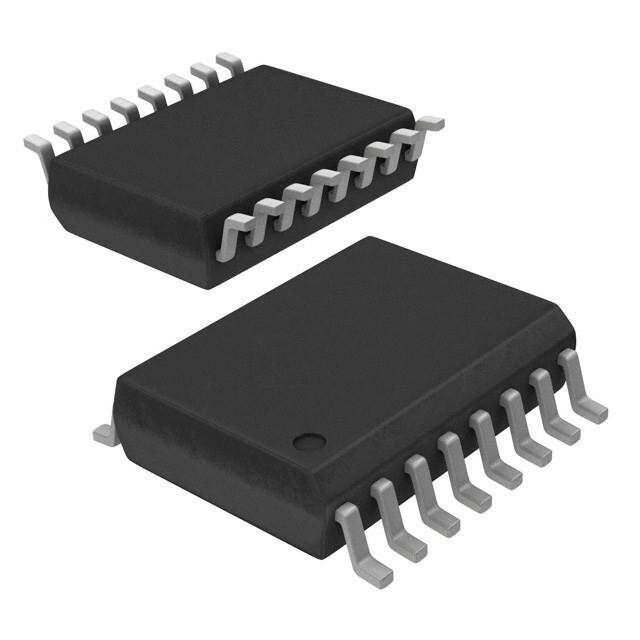
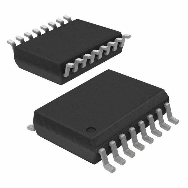
| 产品图片 |
|
| rohs | 符合RoHS无铅 / 符合限制有害物质指令(RoHS)规范要求 |
| 产品系列 | 接口 IC,数字隔离器,Texas Instruments ISO7231ADW- |
| 数据手册 | |
| 产品型号 | ISO7231ADW |
| PCN设计/规格 | |
| PulseWidthDistortion(Max) | 10ns |
| 上升/下降时间(典型值) | 2ns, 2ns |
| 产品目录页面 | |
| 产品种类 | |
| 传播延迟tpLH/tpHL(最大值) | 95ns, 95ns |
| 传播延迟时间 | 80 ns |
| 供应商器件封装 | 16-SOIC |
| 共模瞬态抗扰度(最小值) | 25kV/µs |
| 其它名称 | 296-22959-5 |
| 制造商产品页 | http://www.ti.com/general/docs/suppproductinfo.tsp?distId=10&orderablePartNumber=ISO7231ADW |
| 包装 | 管件 |
| 单位重量 | 420.400 mg |
| 商标 | Texas Instruments |
| 安装风格 | SMD/SMT |
| 封装 | Tube |
| 封装/外壳 | 16-SOIC(0.295",7.50mm 宽) |
| 封装/箱体 | SOIC-16 Wide |
| 工作温度 | -40°C ~ 125°C |
| 工厂包装数量 | 40 |
| 技术 | 容性耦合 |
| 数据速率 | 1Mbps |
| 最大工作温度 | + 125 C |
| 最大数据速率 | 1 Mb/s |
| 最小工作温度 | - 40 C |
| 标准包装 | 40 |
| 电压-电源 | 3.15 V ~ 5.5 V |
| 电压-隔离 | 4000Vpk |
| 类型 | General Purpose |
| 系列 | ISO7231A |
| 绝缘电压 | 4 kVrms |
| 脉宽失真(最大) | 10ns |
| 输入-输入侧1/输入侧2 | 2/1 |
| 通道数 | 3 |
| 通道数量 | 3 Channel |
| 通道类型 | 单向 |
| 配用 | /product-detail/zh/ISO723X724XEVM/296-30949-ND/1898682 |
| 隔离式电源 | 无 |

.jpg)


- 商务部:美国ITC正式对集成电路等产品启动337调查
- 曝三星4nm工艺存在良率问题 高通将骁龙8 Gen1或转产台积电
- 太阳诱电将投资9.5亿元在常州建新厂生产MLCC 预计2023年完工
- 英特尔发布欧洲新工厂建设计划 深化IDM 2.0 战略
- 台积电先进制程称霸业界 有大客户加持明年业绩稳了
- 达到5530亿美元!SIA预计今年全球半导体销售额将创下新高
- 英特尔拟将自动驾驶子公司Mobileye上市 估值或超500亿美元
- 三星加码芯片和SET,合并消费电子和移动部门,撤换高东真等 CEO
- 三星电子宣布重大人事变动 还合并消费电子和移动部门
- 海关总署:前11个月进口集成电路产品价值2.52万亿元 增长14.8%
PDF Datasheet 数据手册内容提取
Not Recommended for New Designs ISO7230A ISO7231A www.ti.com SLLS906C–MAY2008–REVISEDJUNE2011 One Megabit per Second Triple Digital Isolators CheckforSamples:ISO7230A,ISO7231A FEATURES 1 • 1MbpsSignalingRate • HighElectromagneticImmunity – LowChannel-to-ChannelOutputSkew; (SeeApplicationnoteSLLA181) 2nsMaximum(5V-Operation) • –40°Cto125°COperatingRange – LowPulse-WidthDistortion(PWD); APPLICATIONS 10nsMaximum(5V-Operation) • Typical25-YearLifeatRatedWorkingVoltage • IndustrialFieldbus (SeeApplicationnoteSLLA197andFigure10) • ComputerPeripheralInterface • 4000VpeakIsolation,560VpeakVIORM • ServoControlInterface – UL1577,IEC60747-5-2(VDE0884,Rev2), • DataAcquisition IE61010-1andCSAApproved,IEC60950-1 • 4kVESDProtection • OperateWith3.3Vor5VSupplies DESCRIPTION See the Product Notification section. The ISO7230A and ISO7231A are triple-channel digital isolators each with multiple channel configurations and output-enable functions. These devices have logic input and output buffers separated by TI’s silicon dioxide (SiO ) isolation barrier. Used in conjunction with isolated power supplies, these 2 devices block high voltage, isolate grounds, and prevent noise currents on a data bus or other circuits from enteringthelocalgroundandinterferingwithordamagingsensitivecircuitry. The ISO7230 triple-channel device has all three channels in the same direction while the ISO7231 has two channels in one direction and one channel in opposition. These devices have an active-high output enable that whendriventoalowlevel,placestheoutputinahigh-impedancestate. The ISO7230A and ISO7231A have TTL input thresholds and a noise-filter at the input that prevents transient pulsesofupto2nsindurationfrombeingpassedtotheoutputofthedevice. In each device a periodic update pulse is sent across the isolation barrier to ensure the proper dc level of the output.Ifthisdc-refreshpulseisnotreceived,theinputisassumedtobeunpoweredornotbeingactivelydriven, andthefailsafecircuitdrivestheoutputtoalogichighstate.(ContactTIforalogiclowfailsafeoption). These devices require two supply voltages of 3.3V, 5V, or any combination. All inputs are 5V tolerant when supplied from a 3.3V supply and all outputs are 4mA CMOS. These devices are characterized for operation over theambienttemperaturerangeof–40°Cto125°C. ISO7230 ISO7231 DW PACKAGE DW PACKAGE VCC1 1 16 VCC2 VCC1 1 16 VCC2 GND1 2 15 GND2 GND1 2 15 GND2 INA 3 14 OUTA INA 3 14 OUTA INB 4 13 OUTB INB 4 13 OUTB INC 5 12 OUTC OUTC 5 12 INC NC 6 11 NC NC 6 11 NC NC 7 10 EN EN1 7 10 EN2 GND1 8 9 GND2 GND1 8 9 GND2 1 Pleasebeawarethatanimportantnoticeconcerningavailability,standardwarranty,anduseincriticalapplicationsofTexas Instrumentssemiconductorproductsanddisclaimerstheretoappearsattheendofthisdatasheet. PRODUCTIONDATAinformationiscurrentasofpublicationdate. Copyright©2008–2011,TexasInstrumentsIncorporated Products conform to specifications per the terms of the Texas Instruments standard warranty. Production processing does not necessarilyincludetestingofallparameters.
Not Recommended for New Designs ISO7230A ISO7231A SLLS906C–MAY2008–REVISEDJUNE2011 www.ti.com This integrated circuit can be damaged by ESD. Texas Instruments recommends that all integrated circuits be handled with appropriateprecautions.Failuretoobserveproperhandlingandinstallationprocedurescancausedamage. ESDdamagecanrangefromsubtleperformancedegradationtocompletedevicefailure.Precisionintegratedcircuitsmaybemore susceptibletodamagebecauseverysmallparametricchangescouldcausethedevicenottomeetitspublishedspecifications. FUNCTION DIAGRAM Galvanic Isolation Barrier DC Channel Filter OSC + Vref Pulse Width Demodulation PWM Carrier Detect EN Input Data MUX AC Detect IN + Vref OUT Filter Output Buffer AC Channel Table1.DeviceFunctionTableISO723x (1) INPUT OUTPUTENABLE OUTPUT INPUTV OUTPUTV CC CC (IN) (EN) (OUT) H HorOpen H L HorOpen L PU PU X L Z Open HorOpen H PD PU X HorOpen H PD PU X L Z (1) PU=PoweredUp;PD=PoweredDown;X=Irrelevant;H=HighLevel;L=LowLevel AVAILABLEOPTIONS SIGNALING INPUT CHANNEL MARKED ORDERING PRODUCT RATE THRESHOLD CONFIGURATION AS NUMBER(1) ~1.5V(TTL) ISO7230ADW(rail) ISO7230ADW 1Mbps 3/0 ISO7230A (CMOScompatible) ISO7230ADWR(reel) ~1.5V(TTL) ISO7231ADW(rail) ISO7231ADW 1Mbps 2/1 ISO7231A (CMOScompatible) ISO7231ADWR(reel) (1) Forthemostcurrentpackageandorderinginformation,seethePackageOptionAddendumattheendofthisdocument,orseetheTI websiteatwww.ti.com. 2 Copyright©2008–2011,TexasInstrumentsIncorporated
Not Recommended for New Designs ISO7230A ISO7231A www.ti.com SLLS906C–MAY2008–REVISEDJUNE2011 ABSOLUTE MAXIMUM RATINGS(1) VALUE UNIT V Supplyvoltage(2),V ,V –0.5to6 V CC CC1 CC2 V VoltageatIN,OUT,EN –0.5to6 V I I Outputcurrent ±15 mA O HumanBodyModel JEDECStandard22,TestMethodA114-C.01 ±4 Electrostatic Field-Induced-ChargedDevice kV ESD JEDECStandard22,TestMethodC101 Allpins ±1 discharge Model MachineModel ANSI/ESDS5.2-1996 ±200 V T Maximumjunctiontemperature 170 °C J (1) Stressesbeyondthoselistedunderabsolutemaximumratingsmaycausepermanentdamagetothedevice.Thesearestressratings onlyandfunctionaloperationofthedeviceattheseoranyotherconditionsbeyondthoseindicatedunderrecommendedoperating conditionsisnotimplied.Exposuretoabsolute-maximum-ratedconditionsforextendedperiodsmayaffectdevicereliability. (2) Allvoltagevaluesarewithrespecttonetworkgroundterminalandarepeakvoltagevalues. RECOMMENDED OPERATING CONDITIONS MIN TYP MAX UNIT V Supplyvoltage(1),V ,V 3.15 5.5 V CC CC1 CC2 I High-leveloutputcurrent –4 mA OH I Low-leveloutputcurrent 4 mA OL t Inputpulsewidth 1 μs ui 1/t Signalingrate 0 1500(2) 1000 kbps ui V High-levelinputvoltage(IN)(ENonalldevices) 2 V IH CC V V Low-levelinputvoltage(IN)(ENonalldevices) 0 0.8 IL T Junctiontemperature 150 °C J Externalmagneticfield-strengthimmunityperIEC61000-4-8andIEC61000-4-9 H 1000 A/m certification (1) Forthe5Voperation,V orV isspecifiedfrom4.5Vto5.5V. CC1 CC2 Forthe3Voperation,V orV isspecifiedfrom3.15Vto3.6V. CC1 CC2 (2) Typicalsignalingrateunderidealconditionsat25°C. Copyright©2008–2011,TexasInstrumentsIncorporated 3
Not Recommended for New Designs ISO7230A ISO7231A SLLS906C–MAY2008–REVISEDJUNE2011 www.ti.com ELECTRICAL CHARACTERISTICS: V and V at 5V(1) OPERATION CC1 CC2 overrecommendedoperatingconditions(unlessotherwisenoted) PARAMETER TESTCONDITIONS MIN TYP MAX UNIT SUPPLYCURRENT Quiescent V =V or0V,Allchannels,noload, 1 3 ISO7230A I CC mA 1Mbps EN2at3V 1 3 I CC1 Quiescent V =V or0V,Allchannels,noload, 6.5 11 ISO7231A I CC mA 1Mbps EN1at3V,EN2at3V 6.5 11 Quiescent V =V or0V,Allchannels,noload, 15 22 ISO7230A I CC mA 1Mbps EN2at3V 16 22 I CC2 Quiescent V =V or0V,Allchannels,noload, 13 20 ISO7231A I CC mA 1Mbps EN1at3V,EN2at3V 13 20 ELECTRICALCHARACTERISTICS I Sleepmodeoutputcurrent ENat0V,Singlechannel 0 μA OFF I =–4mA,SeeFigure1 V –0.8 OH CC V High-leveloutputvoltage V OH I =–20μA,SeeFigure1 V –0.1 OH CC I =4mA,SeeFigure1 0.4 OL V Low-leveloutputvoltage V OL I =20μA,SeeFigure1 0.1 OL V Inputvoltagehysteresis 150 mV I(HYS) I High-levelinputcurrent 10 IH INfrom0VtoV μA CC I Low-levelinputcurrent –10 IL C Inputcapacitancetoground INatV ,V =0.4sin(4E6πt) 2 pF I CC I CMTI Common-modetransientimmunity V =V or0V,SeeFigure4 25 50 kV/μs I CC (1) Forthe5Voperation,V orV isspecifiedfrom4.5Vto5.5V. CC1 CC2 Forthe3Voperation,V orV isspecifiedfrom3.15Vto3.6V. CC1 CC2 SWITCHING CHARACTERISTICS: V and V at 5V OPERATION CC1 CC2 overrecommendedoperatingconditions(unlessotherwisenoted) PARAMETER TESTCONDITIONS MIN TYP MAX UNIT t ,t Propagationdelay 40 95 PLH PHL SeeFigure1 ns PWD Pulse-widthdistortion(1)|t –t | 10 PHL PLH t Channel-to-channeloutputskew (2) 0 2 ns sk(o) t Outputsignalrisetime 2 r SeeFigure1 ns t Outputsignalfalltime 2 f t Propagationdelay,high-level-to-high-impedanceoutput 15 20 PHZ t Propagationdelay,high-impedance-to-high-leveloutput 15 20 PZH SeeFigure2 ns t Propagationdelay,low-level-to-high-impedanceoutput 15 20 PLZ t Propagationdelay,high-impedance-to-low-leveloutput 15 20 PZL t Failsafeoutputdelaytimefrominputpowerloss SeeFigure3 12 μs fs (1) Alsoreferredtoaspulseskew. (2) t istheskewbetweenspecifiedoutputsofasingledevicewithalldrivinginputsconnectedtogetherandtheoutputsswitchinginthe sk(o) samedirectionwhiledrivingidenticalspecifiedloads. 4 Copyright©2008–2011,TexasInstrumentsIncorporated
Not Recommended for New Designs ISO7230A ISO7231A www.ti.com SLLS906C–MAY2008–REVISEDJUNE2011 ELECTRICAL CHARACTERISTICS: V at 5V, V at 3.3V(1) OPERATION CC1 CC2 overrecommendedoperatingconditions(unlessotherwisenoted) PARAMETER TESTCONDITIONS MIN TYP MAX UNIT SUPPLYCURRENT Quiescent 1 3 ISO7230A V =V or0V,Allchannels,noload,EN at3V mA I CC 2 1Mbps 1 3 I CC1 Quiescent V =V or0V,Allchannels,noload,EN at3V, 6.5 11 ISO7231A I CC 1 mA 1Mbps EN2at3V 6.5 11 Quiescent 9 15 ISO7230A V =V or0V,Allchannels,noload,EN at3V mA I CC 2 1Mbps 9.5 15 I CC2 Quiescent V =V or0V,Allchannels,noload,EN at3V, 8 12 ISO7231A I CC 1 mA 1Mbps EN2at3V 8 12 ELECTRICALCHARACTERISTICS I Sleepmodeoutputcurrent ENat0V,Singlechannel 0 μA OFF ISO7230 V –0.4 CC IOH=–4mA,SeeFigure1 ISO7231 V High-leveloutputvoltage V –0.8 V OH (5-Vside) CC I =–20μA,SeeFigure1 V –0.1 OH CC I =4mA,SeeFigure1 0.4 OL V Low-leveloutputvoltage V OL I =20μA,SeeFigure1 0.1 OL V Inputvoltagehysteresis 150 mV I(HYS) I High-levelinputcurrent 10 IH INfrom0VtoV μA CC I Low-levelinputcurrent –10 IL C Inputcapacitancetoground INatV ,V =0.4sin(4E6πt) 2 pF I CC I Common-modetransient CMTI V =V or0V,SeeFigure4 25 50 kV/μs immunity I CC (1) Forthe5-Voperation,V orV isspecifiedfrom4.5Vto5.5V. CC1 CC2 Forthe3Voperation,V orV isspecifiedfrom3.15Vto3.6V. CC1 CC2 SWITCHING CHARACTERISTICS: V at 5V, V at 3.3V OPERATION CC1 CC2 overrecommendedoperatingconditions(unlessotherwisenoted) PARAMETER TESTCONDITIONS MIN TYP MAX UNIT t ,t Propagationdelay,low-to-high-leveloutput 40 100 PLH PHL ISO723xA SeeFigure1 ns PWD Pulse-widthdistortion(1)|t –t | 11 PHL PLH t Channel-to-channeloutputskew (2) ISO723xA 0 2.5 ns sk(o) t Outputsignalrisetime 2 r SeeFigure1 ns t Outputsignalfalltime 2 f t Propagationdelay,high-level-to-high-impedanceoutput 15 20 PHZ t Propagationdelay,high-impedance-to-high-leveloutput 15 20 PZH SeeFigure2 ns t Propagationdelay,low-level-to-high-impedanceoutput 15 20 PLZ t Propagationdelay,high-impedance-to-low-leveloutput 15 20 PZL t Failsafeoutputdelaytimefrominputpowerloss SeeFigure3 18 μs fs (1) Alsoknownaspulseskew (2) t istheskewbetweenspecifiedoutputsofasingledevicewithalldrivinginputsconnectedtogetherandtheoutputsswitchinginthe sk(o) samedirectionwhiledrivingidenticalspecifiedloads. Copyright©2008–2011,TexasInstrumentsIncorporated 5
Not Recommended for New Designs ISO7230A ISO7231A SLLS906C–MAY2008–REVISEDJUNE2011 www.ti.com ELECTRICAL CHARACTERISTICS: V at 3.3V, V at 5V(1) OPERATION CC1 CC2 overrecommendedoperatingconditions(unlessotherwisenoted) PARAMETER TESTCONDITIONS MIN TYP MAX UNIT SUPPLYCURRENT Quiescent 0.5 1 ISO7230A V =V or0V,Allchannels,noload,EN at3V mA I CC 2 1Mbps 1 2 I CC1 Quiescent V =V or0V,Allchannels,noload,EN at3V, 4.5 7 ISO7231A I CC 1 mA 1Mbps EN2at3V 4.5 7 Quiescent 15 22 ISO7230A V =V or0V,Allchannels,noload,EN at3V mA I CC 2 1Mbps 16 22 I CC2 Quiescent V =V or0V,Allchannels,noload,EN at3V, 13 20 ISO7231A I CC 1 mA 1Mbps EN2at3V 13 20 ELECTRICALCHARACTERISTICS I Sleepmodeoutputcurrent ENat0V,Singlechannel 0 μA OFF ISO7230 V –0.4 CC IOH=–4mA,SeeFigure1 ISO7231 V High-leveloutputvoltage V –0.8 V OH (5-Vside) CC I =–20μA,SeeFigure1 V –0.1 OH CC I =4mA,SeeFigure1 0.4 OL V Low-leveloutputvoltage V OL I =20μA,SeeFigure1 0.1 OL V Inputvoltagehysteresis 150 mV I(HYS) I High-levelinputcurrent 10 IH INfrom0VtoV μA CC I Low-levelinputcurrent –10 IL C Inputcapacitancetoground INatV ,V =0.4sin(4E6πt) 2 pF I CC I Common-modetransient V =V or0V,SeeFigure4 CMTI I CC 25 50 kV/μs immunity (1) For5Voperation,V orV isspecifiedfrom4.5Vto5.5V. CC1 CC2 For3Voperation,V orV isspecifiedfrom3.15Vto3.6V. CC1 CC2 SWITCHING CHARACTERISTICS: V at 3.3V and V at 5V OPERATION CC1 CC2 overrecommendedoperatingconditions(unlessotherwisenoted) PARAMETER TESTCONDITIONS MIN TYP MAX UNIT tPLH,tPHL Propagationdelay 40 100 ISO723xA SeeFigure1 ns PWD Pulse-widthdistortion(1)|tPHL–tPLH| 11 tsk(o) Channel-to-channeloutputskew(2) ISO723xA 0 2.5 ns tr Outputsignalrisetime 2 SeeFigure1 ns tf Outputsignalfalltime 2 tPHZ Propagationdelay,high-level-to-high-impedanceoutput 15 20 tPZH Propagationdelay,high-impedance-to-high-leveloutput 15 20 SeeFigure2 ns tPLZ Propagationdelay,low-level-to-high-impedanceoutput 15 20 tPZL Propagationdelay,high-impedance-to-low-leveloutput 15 20 tfs Failsafeoutputdelaytimefrominputpowerloss SeeFigure3 12 μs (1) Alsoknownaspulseskew (2) t istheskewbetweenspecifiedoutputsofasingledevicewithalldrivinginputsconnectedtogetherandtheoutputsswitchinginthe sk(o) samedirectionwhiledrivingidenticalspecifiedloads. 6 Copyright©2008–2011,TexasInstrumentsIncorporated
Not Recommended for New Designs ISO7230A ISO7231A www.ti.com SLLS906C–MAY2008–REVISEDJUNE2011 ELECTRICAL CHARACTERISTICS: V and V at 3.3V(1) OPERATION CC1 CC2 overrecommendedoperatingconditions(unlessotherwisenoted) PARAMETER TESTCONDITIONS MIN TYP MAX UNIT SUPPLYCURRENT ISO7230A Quiescent VI=VCCor0V,allchannels,noload, 0.5 1 mA 1Mbps EN2at3V 1 2 ICC1 ISO7231A Quiescent VI=VCCor0V,allchannels,noload, 4.5 7 mA 1Mbps EN1at3V,EN2at3V 4.5 7 ISO7230A Quiescent VI=VCCor0V,allchannels,noload, 9 15 mA 1Mbps EN2at3V 9.5 15 ICC2 ISO7231A Quiescent VI=VCCor0V,allchannels,noload, 8 12 mA 1Mbps EN1at3V,EN2at3V 8 12 ELECTRICALCHARACTERISTICS IOFF Sleepmodeoutputcurrent ENat0V,singlechannel 0 μA IOH=–4mA,SeeFigure1 VCC–0.4 VOH High-leveloutputvoltage V IOH=–20μA,SeeFigure1 VCC–0.1 IOL=4mA,SeeFigure1 0.4 VOL Low-leveloutputvoltage V IOL=20μA,SeeFigure1 0.1 VI(HYS) Inputvoltagehysteresis 150 mV IIH High-levelinputcurrent 10 INfrom0VorVCC μA IIL Low-levelinputcurrent –10 CI Inputcapacitancetoground INatVCC,VI=0.4sin(4E6πt) 2 pF CMTI Common-modetransientimmunity VI=VCCor0V,SeeFigure4 25 50 kV/μs (1) For5Voperation,V orV isspecifiedfrom4.5Vto5.5V. CC1 CC2 For3Voperation,V orV isspecifiedfrom3.15Vto3.6V. CC1 CC2 SWITCHING CHARACTERISTICS: V and V at 3.3-V OPERATION CC1 CC2 overrecommendedoperatingconditions(unlessotherwisenoted) PARAMETER TESTCONDITIONS MIN TYP MAX UNIT tPLH,tPHL Propagationdelay 45 110 ISO723xA SeeFigure1 ns PWD Pulse-widthdistortion(1)|tPHL–tPLH| 12 tsk(o) Channel-to-channeloutputskew(2) ISO723xA 0 3 ns tr Outputsignalrisetime 2 SeeFigure1 ns tf Outputsignalfalltime 2 tPHZ Propagationdelay,high-level-to-high-impedanceoutput 15 20 tPZH Propagationdelay,high-impedance-to-high-leveloutput 15 20 SeeFigure2 ns tPLZ Propagationdelay,low-level-to-high-impedanceoutput 15 20 tPZL Propagationdelay,high-impedance-to-low-leveloutput 15 20 tfs Failsafeoutputdelaytimefrominputpowerloss SeeFigure3 18 μs (1) Alsoreferredtoaspulseskew. (2) t istheskewbetweenspecifiedoutputsofasingledevicewithalldrivinginputsconnectedtogetherandtheoutputsswitchinginthe sk(o) samedirectionwhiledrivingidenticalspecifiedloads. Copyright©2008–2011,TexasInstrumentsIncorporated 7
Not Recommended for New Designs ISO7230A ISO7231A SLLS906C–MAY2008–REVISEDJUNE2011 www.ti.com PARAMETER MEASUREMENT INFORMATION ER VCC RRI VI VCC/2 VCC/2 A IN B OUT 0 V Input TION tPLH tPHL GNeOneTrEatAor VI 50W SOLA VO NCOLTE B VO 50% 90% 50%VOH I tr 10% tf VOL A. The input pulse is supplied by a generator having the following characteristics: PRR ≤ 50kHz, 50% duty cycle, t ≤ r 3ns,t ≤3ns,Z =50Ω. f O B. C =15pFandincludesinstrumentationandfixturecapacitancewithin±20%. L Figure1. SwitchingCharacteristicTestCircuitandVoltageWaveforms V cc Vcc 0 V IN ATIONBARRIER OUT RLV=O 1 kW±1% VI tPZL Vcc/2 tPLZ Vcc/2 0VcVc ISOL EN CL VO 50% 0.5V Input NOTE V OL Generator VI 50W B NOTEA R Vcc E IN ARRI OUT VO VI Vcc/2 Vcc/2 3 V NB 0V O TI t ISOLA EN CL RL= 1 kW±V1%O PZH 50% 0.5V VOH Input NOTE 0V Generator VI 50W B tPHZ NOTEA A. The input pulse is supplied by a generator having the following characteristics: PRR ≤ 50kHz, 50% duty cycle, t ≤ r 3ns,t ≤3ns,Z =50Ω. f O B. C =15pFandincludesinstrumentationandfixturecapacitancewithin±20%. L Figure2. Enable/DisablePropagationDelayTimeTestCircuitandWaveform 8 Copyright©2008–2011,TexasInstrumentsIncorporated
Not Recommended for New Designs ISO7230A ISO7231A www.ti.com SLLS906C–MAY2008–REVISEDJUNE2011 PARAMETER MEASUREMENT INFORMATION (continued) V I V CC RIER VCC 0o Vr IN N BAR OUT VO VI 2.7 V 0 V VCC ATIO tfs VOH SOL CL VO 50% I NOTE B V OL A. The input pulse is supplied by a generator having the following characteristics: PRR ≤ 50kHz, 50% duty cycle, t ≤ r 3ns,t ≤3ns,Z =50Ω. f O B. C =15pFandincludesinstrumentationandfixturecapacitancewithin±20%. L Figure3. FailsafeDelayTimeTestCircuitandVoltageWaveforms VCC1 VCC2 C = 0.1mF± 1% C = 0.1mF± 1% R E Pass-fail criteria: RRI Output must IN BA OUT remain stable S1 N O TI A OL NOTE B VOHor VOL S I GND1 GND2 VCM A. The input pulse is supplied by a generator having the following characteristics: PRR ≤ 50kHz, 50% duty cycle, t ≤ r 3ns,t ≤3ns,Z =50Ω. f O B. C =15pFandincludesinstrumentationandfixturecapacitancewithin±20%. L Figure4. Common-ModeTransientImmunityTestCircuitandVoltageWaveform Copyright©2008–2011,TexasInstrumentsIncorporated 9
Not Recommended for New Designs ISO7230A ISO7231A SLLS906C–MAY2008–REVISEDJUNE2011 www.ti.com DEVICE INFORMATION PACKAGE CHARACTERISTICS PARAMETER TESTCONDITIONS MIN TYP MAX UNIT L(I01) Minimumairgap(Clearance) Shortestterminal-to-terminaldistancethroughair 8.34 mm Shortestterminal-to-terminaldistanceacrossthe L(I02) Minimumexternaltracking(Creepage) 8.1 mm packagesurface MinimumInternalGap(Internal Distancethroughtheinsulation 0.008 mm Clearance) Inputtooutput,V =500V,allpinsoneachsideofthe IO barriertiedtogethercreatingatwo-terminaldevice, >1012 Ω RIO Isolationresistance TA<100°C Inputtooutput,V =500V,100°C≤T ≤T max >1011 Ω IO A A C BarriercapacitanceInputtooutput V =0.4sin(4E6πt) 2 pF IO I C Inputcapacitancetoground V =0.4sin(4E6πt) 2 pF I I REGULATORY INFORMATION VDE CSA UL Recognizedunder1577 CertifiedaccordingtoIEC ApprovedunderCSAComponent ComponentRecognition 60747-5-2 AcceptanceNotice Program(1) FileNumber:40016131 FileNumber:220991 FileNumber:E181974 (1) Productiontested≥3000VRMSfor1secondinaccordancewithUL1577. DEVICE I/O SCHEMATICS Enable Input Output V VCC2 VCC2 VCC2 VCC1 VCC1 VCC1 CC2 1 MW 1 MW 500W 500W 8W EN IN OUT 13W 10 Copyright©2008–2011,TexasInstrumentsIncorporated
Not Recommended for New Designs ISO7230A ISO7231A www.ti.com SLLS906C–MAY2008–REVISEDJUNE2011 THERMAL CHARACTERISTICS overrecommendedoperatingconditions(unlessotherwisenoted) PARAMETER TESTCONDITIONS MIN TYP MAX UNIT Low-KThermalResistance(1) 168 θ Junction-to-air °C/W JA High-KThermalResistance 96.1 θ Junction-to-BoardThermalResistance 61 °C/W JB θ Junction-to-CaseThermalResistance 48 °C/W JC V =V =5.5V,T =150°C,C =15pF, P DevicePowerDissipation CC1 CC2 J L 220 mW D Inputa50%dutycyclesquarewave (1) TestedinaccordancewiththeLow-KorHigh-KthermalmetricdefinitionsofEIA/JESD51-3forleadedsurfacemountpackages. TYPICAL CHARACTERISTIC CURVES INPUTTHRESHOLDVOLTAGE V FAILSAFETHRESHOLD CC1 vs vs FREE-AIRTEMPERATURE FREE-AIRTEMPERATURE 1.4 3 5 V V VCCat 5 V or 3.3 V, 1.35 th+ 2.9 Load = 15 pF, Air Flow at 7/cf/m, V 2.8 Low-K Board shold - V 1.12.53 3.3 V Vth+ hreshold - 22..67 Vfs+ ut Voltage Thre 1.11.52 5 V Vth- ALoirw F-lKo wB oaat r7d cf/m, -Failsafe TCC1 222...345 Vfs- p 1.1 V n I 2.2 1.05 3.3 V Vth- 2.1 1 2 -40 -25 -10 5 20 35 50 65 80 95 110 125 -40 -25 -10 5 20 35 50 65 80 95 110 125 TA- Free-Air Temperature -°C TA- Free-Air Temperature -°C Figure5. Figure6. HIGH-LEVELOUTPUTCURRENT LOW-LEVELOUTPUTCURRENT vs vs HIGH-LEVELOUTPUTVOLTAGE LOW-LEVELOUTPUTVOLTAGE 50 50 VCC= 5 V LToAa=d 2 =5 °1C5 pF, 45 LToAa=d 2 =5 °1C5 pF, 40 40 A ut Current - mA 30 VCC= 3.3 V put Current - m 233505 VCC= 3.3 V VCC= 5 V utp 20 Out 20 - OO I- O 15 I 10 10 5 0 0 0 2 4 6 0 1 2 3 4 5 VO- Output Voltage - V VO- Output Voltage - V Figure7. Figure8. Copyright©2008–2011,TexasInstrumentsIncorporated 11
Not Recommended for New Designs ISO7230A ISO7231A SLLS906C–MAY2008–REVISEDJUNE2011 www.ti.com APPLICATION INFORMATION 2 mm 2 mm VCC1 max. from max. from VCC2 VCC1 VCC2 0.1mF 0.1mF 1 16 GND1 GND2 2 15 INA 3 14 OUTA INB 4 13 OUTB INC 5 12 OUTC NC 6 11 NC EN NC 7 10 GND1 GND2 8 9 ISO7230 Figure9. TypicalISO7230ApplicationCircuit LIFE EXPECTANCY vs WORKING VOLTAGE 100 S R A E Y E -- VIORMat 560-V F LI 28Years G N KI R O W 10 0 120 250 500 750 880 1000 WORKING VOLTAGE (V ) -- V IORM Figure10. TimeDependantDielectricBreakdownTestingResults 12 Copyright©2008–2011,TexasInstrumentsIncorporated
Not Recommended for New Designs ISO7230A ISO7231A www.ti.com SLLS906C–MAY2008–REVISEDJUNE2011 PRODUCT NOTIFICATION AnISO723xAanomalyoccurswhenanegative-goingpulsebelowthespecified1μsminimumbitwidthisinputto thedevice.Theoutputlocksinalogic-lowconditionuntilthenextrisingedgeoccursaftera1μsperiod. Positive noise edges in pulses of less than the minimum specified 1μs have no effect on the device, and are properlyfiltered. To prevent noise from interfering with ISO723xA performance, it is recommended that an appropriately sized capacitorbeplacedoneachinputofthedevice Figure11. ISO723xAAnomaly Copyright©2008–2011,TexasInstrumentsIncorporated 13
Not Recommended for New Designs ISO7230A ISO7231A SLLS906C–MAY2008–REVISEDJUNE2011 www.ti.com REVISION HISTORY ChangesfromOriginal(May2008)toRevisionA Page • AddedProductNotificationsectionlink. ............................................................................................................................... 1 • Deletedtextfromparagraph2oftheDescription:"andturnsoffinternalbiascircuitrytoconservepower" ....................... 1 • DeletedProductPreviewnote .............................................................................................................................................. 2 • ChangedFrom:3To:3.15.................................................................................................................................................... 3 • ChangedV From:3.6To:3.45.......................................................................................................................................... 3 CC • ChangedI andI valuesFrom:TBD ............................................................................................................................. 4 CC1 CC2 • ChangedV –0.4To:V –0.8 ......................................................................................................................................... 4 CC CC • ChangedTypicalvaluefrom1To:2..................................................................................................................................... 4 • ChangedPropagationdelaymaxFrom:80To:95 .............................................................................................................. 4 • ChangedI andI valuesFrom:TBD............................................................................................................................. 5 CC1 CC2 • ChangedTypicalvaluefrom1To:2..................................................................................................................................... 5 • ChangedPropagationdelaymaxFrom:80To:100 ............................................................................................................ 5 • ChangedI andI valuesFrom:TBD............................................................................................................................. 6 CC1 CC2 • ChangedTypicalvaluefrom1To:2..................................................................................................................................... 6 • ChangedPropagationdelaymaxFrom:80To:100 ............................................................................................................ 6 • ChangedI andI valuesFrom:TBD............................................................................................................................. 7 CC1 CC2 • Changed ............................................................................................................................................................................... 7 • ChangedTypicalvaluefrom1To:2..................................................................................................................................... 7 • ChangedPropagationdelaymaxFrom:85To:110 ............................................................................................................ 7 • ChangedL(101)Minimumairgap(Clearance)-minimumvaluefrom:7.7mmto:8.34mm .............................................. 10 • ChangedTypicalvaluefrom1To:2................................................................................................................................... 10 • ChangedTypicalvaluefrom1To:2................................................................................................................................... 10 • ChangedtheREGULATORYINFORMATIONTable ......................................................................................................... 10 • ChangedFigure11 ............................................................................................................................................................. 13 ChangesfromRevisionA(June2008)toRevisionB Page • ChangedV From:3.45To:3.6.......................................................................................................................................... 3 CC ChangesfromRevisionB(July2008)toRevisionC Page • Changed"1ns"to"2ns",added"(5v-Operation)".................................................................................................................. 1 • Changed"2ns"to"10ns",added"(5v-Operation)"................................................................................................................ 1 • Deleted"LowJitterContent;1nsTypat150Mbps" ............................................................................................................ 1 • DeletedMin=4.5Vandmax=5.5VforSupplyVoltageoftheROCTable. ..................................................................... 3 • ChangedV From:3.6To:5.5............................................................................................................................................ 3 CC • CorrectedFigure1 ................................................................................................................................................................ 8 • ChangedFilenumber"1698195"to"220991" .................................................................................................................... 10 • CorrectedDEVICEI/OSCHEMATICS ............................................................................................................................... 10 • CorrectedFigure9 .............................................................................................................................................................. 12 14 Copyright©2008–2011,TexasInstrumentsIncorporated
PACKAGE OPTION ADDENDUM www.ti.com 6-Feb-2020 PACKAGING INFORMATION Orderable Device Status Package Type Package Pins Package Eco Plan Lead/Ball Finish MSL Peak Temp Op Temp (°C) Device Marking Samples (1) Drawing Qty (2) (6) (3) (4/5) ISO7230ADW NRND SOIC DW 16 40 Green (RoHS NIPDAU Level-2-260C-1 YEAR -40 to 125 ISO7230A & no Sb/Br) ISO7230ADWG4 NRND SOIC DW 16 40 Green (RoHS NIPDAU Level-2-260C-1 YEAR -40 to 125 ISO7230A & no Sb/Br) ISO7230ADWR NRND SOIC DW 16 2000 Green (RoHS NIPDAU Level-2-260C-1 YEAR -40 to 125 ISO7230A & no Sb/Br) ISO7231ADW NRND SOIC DW 16 40 Green (RoHS NIPDAU Level-2-260C-1 YEAR -40 to 125 ISO7231A & no Sb/Br) ISO7231ADWR NRND SOIC DW 16 2000 Green (RoHS NIPDAU Level-2-260C-1 YEAR -40 to 125 ISO7231A & no Sb/Br) (1) The marketing status values are defined as follows: ACTIVE: Product device recommended for new designs. LIFEBUY: TI has announced that the device will be discontinued, and a lifetime-buy period is in effect. NRND: Not recommended for new designs. Device is in production to support existing customers, but TI does not recommend using this part in a new design. PREVIEW: Device has been announced but is not in production. Samples may or may not be available. OBSOLETE: TI has discontinued the production of the device. (2) RoHS: TI defines "RoHS" to mean semiconductor products that are compliant with the current EU RoHS requirements for all 10 RoHS substances, including the requirement that RoHS substance do not exceed 0.1% by weight in homogeneous materials. Where designed to be soldered at high temperatures, "RoHS" products are suitable for use in specified lead-free processes. TI may reference these types of products as "Pb-Free". RoHS Exempt: TI defines "RoHS Exempt" to mean products that contain lead but are compliant with EU RoHS pursuant to a specific EU RoHS exemption. Green: TI defines "Green" to mean the content of Chlorine (Cl) and Bromine (Br) based flame retardants meet JS709B low halogen requirements of <=1000ppm threshold. Antimony trioxide based flame retardants must also meet the <=1000ppm threshold requirement. (3) MSL, Peak Temp. - The Moisture Sensitivity Level rating according to the JEDEC industry standard classifications, and peak solder temperature. (4) There may be additional marking, which relates to the logo, the lot trace code information, or the environmental category on the device. (5) Multiple Device Markings will be inside parentheses. Only one Device Marking contained in parentheses and separated by a "~" will appear on a device. If a line is indented then it is a continuation of the previous line and the two combined represent the entire Device Marking for that device. (6) Lead/Ball Finish - Orderable Devices may have multiple material finish options. Finish options are separated by a vertical ruled line. Lead/Ball Finish values may wrap to two lines if the finish value exceeds the maximum column width. Addendum-Page 1
PACKAGE OPTION ADDENDUM www.ti.com 6-Feb-2020 Important Information and Disclaimer:The information provided on this page represents TI's knowledge and belief as of the date that it is provided. TI bases its knowledge and belief on information provided by third parties, and makes no representation or warranty as to the accuracy of such information. Efforts are underway to better integrate information from third parties. TI has taken and continues to take reasonable steps to provide representative and accurate information but may not have conducted destructive testing or chemical analysis on incoming materials and chemicals. TI and TI suppliers consider certain information to be proprietary, and thus CAS numbers and other limited information may not be available for release. In no event shall TI's liability arising out of such information exceed the total purchase price of the TI part(s) at issue in this document sold by TI to Customer on an annual basis. Addendum-Page 2
PACKAGE MATERIALS INFORMATION www.ti.com 29-Sep-2019 TAPE AND REEL INFORMATION *Alldimensionsarenominal Device Package Package Pins SPQ Reel Reel A0 B0 K0 P1 W Pin1 Type Drawing Diameter Width (mm) (mm) (mm) (mm) (mm) Quadrant (mm) W1(mm) ISO7230ADWR SOIC DW 16 2000 330.0 16.4 10.75 10.7 2.7 12.0 16.0 Q1 ISO7231ADWR SOIC DW 16 2000 330.0 16.4 10.75 10.7 2.7 12.0 16.0 Q1 PackMaterials-Page1
PACKAGE MATERIALS INFORMATION www.ti.com 29-Sep-2019 *Alldimensionsarenominal Device PackageType PackageDrawing Pins SPQ Length(mm) Width(mm) Height(mm) ISO7230ADWR SOIC DW 16 2000 350.0 350.0 43.0 ISO7231ADWR SOIC DW 16 2000 350.0 350.0 43.0 PackMaterials-Page2
GENERIC PACKAGE VIEW DW 16 SOIC - 2.65 mm max height 7.5 x 10.3, 1.27 mm pitch SMALL OUTLINE INTEGRATED CIRCUIT This image is a representation of the package family, actual package may vary. Refer to the product data sheet for package details. 4224780/A www.ti.com
PACKAGE OUTLINE DW0016B SOIC - 2.65 mm max height SCALE 1.500 SOIC C 10.63 SEATING PLANE TYP 9.97 A PIN 1 ID 0.1 C AREA 14X 1.27 16 1 10.5 2X 10.1 8.89 NOTE 3 8 9 0.51 16X 0.31 7.6 B 7.4 0.25 C A B 2.65 MAX NOTE 4 0.33 TYP 0.10 SEE DETAIL A 0.25 GAGE PLANE 0.3 0 - 8 0.1 1.27 0.40 DETAIL A (1.4) TYPICAL 4221009/B 07/2016 NOTES: 1. All linear dimensions are in millimeters. Dimensions in parenthesis are for reference only. Dimensioning and tolerancing per ASME Y14.5M. 2. This drawing is subject to change without notice. 3. This dimension does not include mold flash, protrusions, or gate burrs. Mold flash, protrusions, or gate burrs shall not exceed 0.15 mm, per side. 4. This dimension does not include interlead flash. Interlead flash shall not exceed 0.25 mm, per side. 5. Reference JEDEC registration MS-013. www.ti.com
EXAMPLE BOARD LAYOUT DW0016B SOIC - 2.65 mm max height SOIC SYMM SYMM 16X (2) 16X (1.65) SEE SEE DETAILS DETAILS 1 1 16 16 16X (0.6) 16X (0.6) SYMM SYMM 14X (1.27) 14X (1.27) 8 9 8 9 R0.05 TYP R0.05 TYP (9.3) (9.75) IPC-7351 NOMINAL HV / ISOLATION OPTION 7.3 mm CLEARANCE/CREEPAGE 8.1 mm CLEARANCE/CREEPAGE LAND PATTERN EXAMPLE SCALE:4X METAL SOLDER MASK SOLDER MASK METAL OPENING OPENING 0.07 MAX 0.07 MIN ALL AROUND ALL AROUND NON SOLDER MASK SOLDER MASK DEFINED DEFINED SOLDER MASK DETAILS 4221009/B 07/2016 NOTES: (continued) 6. Publication IPC-7351 may have alternate designs. 7. Solder mask tolerances between and around signal pads can vary based on board fabrication site. www.ti.com
EXAMPLE STENCIL DESIGN DW0016B SOIC - 2.65 mm max height SOIC SYMM SYMM 16X (2) 16X (1.65) 1 1 16 16 16X (0.6) 16X (0.6) SYMM SYMM 14X (1.27) 14X (1.27) 8 9 8 9 R0.05 TYP R0.05 TYP (9.3) (9.75) IPC-7351 NOMINAL HV / ISOLATION OPTION 7.3 mm CLEARANCE/CREEPAGE 8.1 mm CLEARANCE/CREEPAGE SOLDER PASTE EXAMPLE BASED ON 0.125 mm THICK STENCIL SCALE:4X 4221009/B 07/2016 NOTES: (continued) 8. Laser cutting apertures with trapezoidal walls and rounded corners may offer better paste release. IPC-7525 may have alternate design recommendations. 9. Board assembly site may have different recommendations for stencil design. www.ti.com
IMPORTANTNOTICEANDDISCLAIMER TI PROVIDES TECHNICAL AND RELIABILITY DATA (INCLUDING DATASHEETS), DESIGN RESOURCES (INCLUDING REFERENCE DESIGNS), APPLICATION OR OTHER DESIGN ADVICE, WEB TOOLS, SAFETY INFORMATION, AND OTHER RESOURCES “AS IS” AND WITH ALL FAULTS, AND DISCLAIMS ALL WARRANTIES, EXPRESS AND IMPLIED, INCLUDING WITHOUT LIMITATION ANY IMPLIED WARRANTIES OF MERCHANTABILITY, FITNESS FOR A PARTICULAR PURPOSE OR NON-INFRINGEMENT OF THIRD PARTY INTELLECTUAL PROPERTY RIGHTS. These resources are intended for skilled developers designing with TI products. You are solely responsible for (1) selecting the appropriate TI products for your application, (2) designing, validating and testing your application, and (3) ensuring your application meets applicable standards, and any other safety, security, or other requirements. These resources are subject to change without notice. TI grants you permission to use these resources only for development of an application that uses the TI products described in the resource. Other reproduction and display of these resources is prohibited. No license is granted to any other TI intellectual property right or to any third party intellectual property right. TI disclaims responsibility for, and you will fully indemnify TI and its representatives against, any claims, damages, costs, losses, and liabilities arising out of your use of these resources. TI’s products are provided subject to TI’s Terms of Sale (www.ti.com/legal/termsofsale.html) or other applicable terms available either on ti.com or provided in conjunction with such TI products. TI’s provision of these resources does not expand or otherwise alter TI’s applicable warranties or warranty disclaimers for TI products. Mailing Address: Texas Instruments, Post Office Box 655303, Dallas, Texas 75265 Copyright © 2020, Texas Instruments Incorporated