ICGOO在线商城 > 集成电路(IC) > 数据采集 - 模数转换器 > ADS5231IPAG

 Datasheet下载
- 型号: ADS5231IPAG
- 制造商: Texas Instruments
- 库位|库存: xxxx|xxxx
- 要求:
| 数量阶梯 | 香港交货 | 国内含税 |
| +xxxx | $xxxx | ¥xxxx |
查看当月历史价格
查看今年历史价格
ADS5231IPAG产品简介:
ICGOO电子元器件商城为您提供ADS5231IPAG由Texas Instruments设计生产,在icgoo商城现货销售,并且可以通过原厂、代理商等渠道进行代购。 ADS5231IPAG价格参考¥119.53-¥199.34。Texas InstrumentsADS5231IPAG封装/规格:数据采集 - 模数转换器, 12 Bit Analog to Digital Converter 2 Input 2 Pipelined 64-TQFP (10x10)。您可以下载ADS5231IPAG参考资料、Datasheet数据手册功能说明书,资料中有ADS5231IPAG 详细功能的应用电路图电压和使用方法及教程。
Texas Instruments(德州仪器)的ADS5231IPAG是一款高性能、低功耗的12位模数转换器(ADC),属于数据采集系统中的关键组件。其主要应用场景包括:

1. 通信系统
   ADS5231IPAG适用于无线通信基础设施,例如基站接收器、软件定义无线电(SDR)和多载波GSM/LTE应用。它能够以高达65MSPS的采样速率处理宽带信号,支持多通道数据采集,从而满足现代通信系统的高带宽需求。

2. 医疗成像设备
   在医疗领域,这款ADC可用于超声成像、CT扫描和其他需要高精度数据采集的设备中。其低功耗特性和良好的信噪比(SNR)性能,确保了图像质量和设备的高效运行。

3. 工业自动化与控制
   ADS5231IPAG适合工业自动化中的精密测量和控制系统,例如振动分析、过程监控和电机控制。其多通道设计可以同时采集多个传感器信号,提高系统的实时性和效率。

4. 测试与测量仪器
   在示波器、频谱分析仪等测试设备中,该ADC能够提供快速而准确的信号转换能力,帮助工程师捕捉和分析复杂的模拟信号。

5. 雷达与国防应用
   由于其出色的动态范围和线性度,ADS5231IPAG也广泛应用于雷达系统和国防电子设备中,用于目标检测和跟踪。

总之,ADS5231IPAG凭借其高分辨率、低功耗和多通道特性,成为需要高速数据采集和精确信号处理的各种应用的理想选择。
| 参数 | 数值 |
| 产品目录 | 集成电路 (IC) |
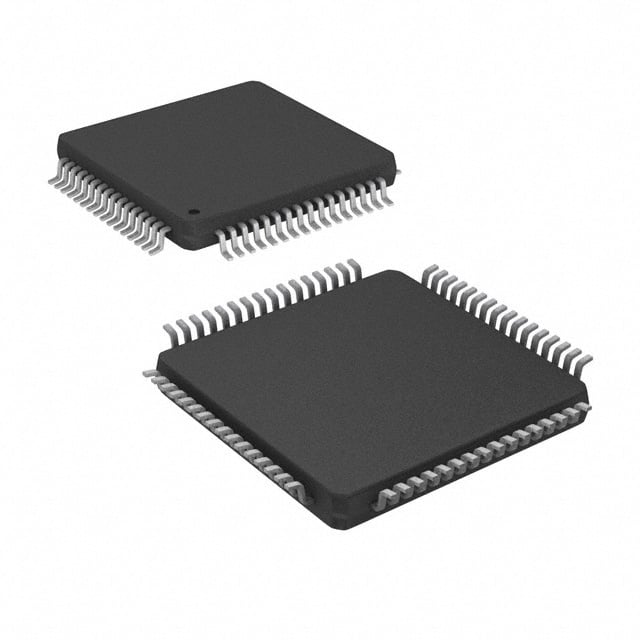
| 描述 | IC ADC 12BIT 40MSPS DUAL 64-TQFP |
| 产品分类 | |
| 品牌 | Texas Instruments |
| 数据手册 | |
| 产品图片 |
|
| 产品型号 | ADS5231IPAG |
| rohs | 无铅 / 符合限制有害物质指令(RoHS)规范要求 |
| 产品系列 | - |
| 产品培训模块 | http://www.digikey.cn/PTM/IndividualPTM.page?site=cn&lang=zhs&ptm=13240 |
| 产品目录页面 | |
| 位数 | 12 |
| 供应商器件封装 | 64-TQFP(10x10) |
| 其它名称 | 296-21529 |
| 制造商产品页 | http://www.ti.com/general/docs/suppproductinfo.tsp?distId=10&orderablePartNumber=ADS5231IPAG |
| 包装 | 托盘 |
| 安装类型 | 表面贴装 |
| 封装/外壳 | 64-TQFP |
| 工作温度 | -40°C ~ 85°C |
| 数据接口 | 串行 |
| 标准包装 | 160 |
| 特性 | 同步采样 |
| 电压源 | 单电源 |
| 转换器数 | 2 |
| 输入数和类型 | 2 个差分,单极 |
| 配用 | /product-detail/zh/ADS5231EVM/ADS5231EVM-ND/1895615 |
| 采样率(每秒) | 40M |


- 商务部:美国ITC正式对集成电路等产品启动337调查
- 曝三星4nm工艺存在良率问题 高通将骁龙8 Gen1或转产台积电
- 太阳诱电将投资9.5亿元在常州建新厂生产MLCC 预计2023年完工
- 英特尔发布欧洲新工厂建设计划 深化IDM 2.0 战略
- 台积电先进制程称霸业界 有大客户加持明年业绩稳了
- 达到5530亿美元!SIA预计今年全球半导体销售额将创下新高
- 英特尔拟将自动驾驶子公司Mobileye上市 估值或超500亿美元
- 三星加码芯片和SET,合并消费电子和移动部门,撤换高东真等 CEO
- 三星电子宣布重大人事变动 还合并消费电子和移动部门
- 海关总署:前11个月进口集成电路产品价值2.52万亿元 增长14.8%


PDF Datasheet 数据手册内容提取
(cid:2)(cid:17)(cid:14)(cid:14)(cid:20)(cid:2)(cid:14)(cid:13)(cid:18)(cid:12) (cid:4)(cid:14)(cid:13)(cid:8)(cid:17)(cid:7)(cid:16)(cid:15) ADS5231 (cid:10)(cid:14)(cid:13)(cid:11) (cid:5)(cid:9)(cid:19)(cid:6)(cid:15) (cid:3)(cid:12)(cid:15)(cid:16)(cid:14)(cid:17)(cid:11)(cid:9)(cid:12)(cid:16)(cid:15) SBAS295A–JULY2004–REVISEDJANUARY2007 Dual, 12-Bit, 40MSPS, +3.3V Analog-to-Digital Converter FEATURES DESCRIPTION • Single+3.3VSupply The ADS5231 is a dual, high-speed, high dynamic • HighSNR:70.7dBFSatf =5MHz range, 12-bit pipelined analog-to-digital converter IN • TotalPowerDissipation: (ADC). This converter includes a high-bandwidth sample-and-hold amplifier that gives excellent InternalReference:321mW spurious performance up to and beyond the Nyquist ExternalReference:285mW rate. The differential nature of the sample-and-hold • InternalorExternalReference amplifier and ADC circuitry minimizes even-order • LowDNL:– 0.3LSB harmonics and gives excellent common-mode noise immunity. • FlexibleInputRange:1.5V to2V PP PP • TQFP-64Package The ADS5231 provides for setting the full-scale range of the converter without any external reference circuitry. The internal reference can be disabled, APPLICATIONS allowing low-drive, external references to be used for • CommunicationsIFProcessing improvedtrackinginmultichannelsystems. • CommunicationsBaseStations The ADS5231 provides an over-range indicator flag • TestEquipment to indicate an input signal that exceeds the full-scale • MedicalImaging input range of the converter. This flag can be used to • VideoDigitizing reduce the gain of front-end gain control circuitry. • CCDDigitizing There is also an output enable pin to allow for multiplexing and testing on a printed circuit board (PCB). The ADS5231 employs digital error correction techniques to provide excellent differential linearity fordemandingimaging applications. The ADS5231 is availableinaTQFP-64package. AVDD SDATASEN SCLK SEL VDRV OEA ADS5231 Serial Interface DISABLE_PLL VIN IINNAA S/H Pi1pA2eD-lBiCnietd CoLErrorergocictrion 3O-uSttpautet DD10···1AA OVRA DVA INT/EXT RIenfteerrennacle TimAindgju/Dstu (tPy LCLy)cle CLK CM REFT REFB DVB VIN IINNBB S/H Pi1pA2eD-lBiCnietd CoLErrorergocictrion 3O-uSttpautet DD10···1BB OVRB STPD OEB Pleasebeawarethatanimportantnoticeconcerningavailability,standardwarranty,anduseincriticalapplicationsofTexas Instrumentssemiconductorproductsanddisclaimerstheretoappearsattheendofthisdatasheet. Alltrademarksarethepropertyoftheirrespectiveowners. PRODUCTIONDATAinformationiscurrentasofpublicationdate. Copyright©2004–2007,TexasInstrumentsIncorporated Products conform to specifications per the terms of the Texas Instruments standard warranty. Production processing does not necessarilyincludetestingofallparameters.
ADS5231 www.ti.com SBAS295A–JULY2004–REVISEDJANUARY2007 This integrated circuit can be damaged by ESD. Texas Instruments recommends that all integrated circuits be handled with appropriateprecautions.Failuretoobserveproperhandlingandinstallationprocedurescancausedamage. ESD damage can range from subtle performance degradation to complete device failure. Precision integrated circuits may be more susceptible to damage because very small parametric changes could cause the device not to meet its published specifications. ORDERINGINFORMATION(1) SPECIFIED PACKAGE TEMPERATURE PACKAGE ORDERING TRANSPORT PRODUCT PACKAGE-LEAD DESIGNATOR RANGE MARKING NUMBER MEDIA,QUANTITY ADS5231IPAG Tray,160 ADS5231 TQFP-64 PAG –40(cid:176) Cto+85(cid:176) C ADS5231IPAG ADS5231IPAGT TapeandReel,250 (1) ForthemostcurrentpackageandorderinginformationseethePackageOptionAddendumattheendofthisdocument,orseetheTI websiteatwww.ti.com. ABSOLUTE MAXIMUM RATINGS(1) SupplyVoltageRange,AVDD –0.3Vto+3.8V SupplyVoltageRange,VDRV –0.3Vto+3.8V VoltageBetweenAVDDandVDRV –0.3Vto+0.3V VoltageAppliedtoExternalREFPins –0.3Vto+2.4V AnalogInputPins(2) –0.3Vtomin.[3.3V,(AVDD+0.3V)] CaseTemperature +100(cid:176) C OperatingFree-AirTemperatureRange,T –40(cid:176) Cto+85(cid:176) C A LeadTemperature +260(cid:176) C JunctionTemperature +105(cid:176) C StorageTemperature –65(cid:176) Cto+150(cid:176) C (1) StressesabovethoselistedunderAbsoluteMaximumRatingsmaycausepermanentdamagetothedevice.Exposuretoabsolute maximumconditionsforextendedperiodsmayaffectdevicereliability. (2) Thedcvoltageappliedontheinputpinsshouldnotgobelow–0.3V.Also,thedcvoltageshouldbelimitedtothelowerofeither3.3Vor (AVDD+0.3V).Iftheinputcangohigherthan+3.3V,thenaresistorgreaterthanorequalto25W shouldbeaddedinserieswitheach oftheinputpins.Also,thedutycycleoftheovershootbeyond+3.3Vshouldbelimited.Theovershootdutycyclecanbedefinedeither asapercentageofthetimeofovershootoveraclockperiod,orovertheentiredevicelifetime.Forapeakvoltagebetween+3.3Vand +3.5V,adutycycleupto10%isacceptable.Forapeakvoltagebetween+3.5Vand+3.7V,theovershootdutycycleshouldnotexceed 1%.Anyovershootbeyond+3.7Vshouldberestrictedtolessthan0.1%dutycycle,andneverexceed+3.9V. 2 SubmitDocumentationFeedback
ADS5231 www.ti.com SBAS295A–JULY2004–REVISEDJANUARY2007 RECOMMENDED OPERATING CONDITIONS ADS5231 MIN TYP MAX UNITS SUPPLIESANDREFERENCES AnalogSupplyVoltage,AVDD 3.0 3.3 3.6 V OutputDriverSupplyVoltage,VDRV 3.0 3.3 3.6 V REF —ExternalReferenceMode 1.875 2.0 2.05 V T REF —ExternalReferenceMode 0.95 1.0 1.125 V B REFCM=(REF +REF )/2–ExternalReferenceMode(1) V – 50mV V T B CM Reference=(REF –REF )–ExternalReferenceMode 0.75 1.0 1.1 V T B AnalogInputCommon-ModeRange(1) V – 50mV V CM CLOCKINPUTANDOUTPUTS ADCLKInputSampleRate PLLEnabled(default) 20 40 MSPS PLLDisabled 2 30(2) MSPS ADCLKDutyCycle PLLEnabled(default) 45 55 MSPS Low-LevelVoltageClockInput 0.6 V High-LevelVoltageClockInput 2.2 V OperatingFree-AirTemperature,T –40 +85 (cid:176) C A ThermalCharacteristics: q 42.8 (cid:176) C/W JA q 18.7 (cid:176) C/W JC (1) Thesevoltagesneedtobesetto1.5V– 50mViftheyarederivedindependentofV . CM (2) WhenthePLLisdisabled,theclockdutycycleneedstobecontrolledwell,especiallyathigherspeeds.A45%–55%dutycyclevariation isacceptableuptoafrequencyof30MSPS.IfthedeviceneedstobeoperatedinthePLLdisabledmodebeyond30MSPS,thenthe dutycycleneedstobemaintainedwithin48%–52%dutycycle. SubmitDocumentationFeedback 3
ADS5231 www.ti.com SBAS295A–JULY2004–REVISEDJANUARY2007 ELECTRICAL CHARACTERISTICS T =–40(cid:176) CandT =+85(cid:176) C.TypicalvaluesareatT =+25(cid:176) C,clockfrequency=40MSPS,50%clockdutycycle, MIN MAX A AVDD=3.3V,VDRV=3.3V,transformer-coupledinputs,–1dBFS,I =56.2kW ,andinternalvoltagereference,unless SET otherwisenoted. ADS5231 PARAMETER TESTCONDITIONS MIN TYP MAX UNITS DCACCURACY NoMissingCodes Tested DNL DifferentialNonlinearity f =5MHz –0.9 – 0.3 +0.9 LSB IN INL IntegralNonlinearity f =5MHz –2.5 – 0.4 +2.5 LSB IN OffsetError(1) –0.75 – 0.2 +0.75 %FS OffsetTemperatureCoefficient(2) – 6 ppm/(cid:176) C FixedAttenuationinChannel(3) 1 %FS FixedAttenuationMatchingAcrossChannels 0.01 0.2 dB GainError/ReferenceError(4) –3.5 – 1.0 +3.5 %FS GainErrorTemperatureCoefficient – 40 ppm/(cid:176) C POWERREQUIREMENTS(5) InternalReference PowerDissipation(5) AnalogOnly(AVDD) 235.5 271 mW OutputDriver(VDRV) 85.5 109 mW TotalPowerDissipation 321 380 mW ExternalReference PowerDissipation AnalogOnly(AVDD) 200 mW OutputDriver(VDRV) 85.5 mW TotalPowerDissipation 285.5 mW TotalPower-Down ClockRunning 83 mW REFERENCEVOLTAGES VREF ReferenceTop(internal) 1.9 2.0 2.1 V T VREF ReferenceBottom(internal) 0.9 1.0 1.1 V B V Common-ModeVoltage 1.4 1.5 1.6 V CM V OutputCurrent(6) – 50mVChangeinVoltage – 2 mA CM VREF ReferenceTop(external) 1.875 V T VREF ReferenceBottom(external) 1.125 V B ExternalReferenceCommon-Mode V – 50mV V CM ExternalReferenceInputCurrent(7) 1.0 mA (1) Offseterroristhedeviationoftheaveragecodefrommid-codewith–1dBFSsinusoidfromidealmid-code(2048).Offseterroris expressedintermsof%offull-scale. (2) IftheoffsetattemperaturesT andT areO andO ,respectively(whereO andO aremeasuredinLSBs),theoffsettemperature 1 2 1 2 1 2 coefficientinppm/(cid:176) Ciscalculatedas(O –O )/(T –T )· 1E6/4096. 1 2 1 2 (3) Fixedattenuationinthechannelarisesbecauseofafixedattenuationinthesample-and-holdamplifier.Whenthedifferentialvoltageat theanaloginputpinsischangedfrom–V to+V ,theswingoftheoutputcodeisexpectedtodeviatefromthefull-scalecode REF REF (4096LSB)bytheextentofthisfixedattenuation.NOTE:V isdefinedas(REF –REF ). REF T B (4) Thereferencevoltagesaretrimmedatproductionsothat(VREF –VREF )iswithin– 35mVoftheidealvalueof1V.Thisspecification T B doesnotincludefixedattenuation. (5) Supplycurrentcanbecalculatedfromdividingthepowerdissipationbythesupplyvoltageof3.3V. (6) TheV outputcurrentspecifiedisthedriveoftheV bufferifloadedexternally. CM CM (7) Averagecurrentdrawnfromthereferencepinsintheexternalreferencemode. 4 SubmitDocumentationFeedback
ADS5231 www.ti.com SBAS295A–JULY2004–REVISEDJANUARY2007 ELECTRICAL CHARACTERISTICS (continued) T =–40(cid:176) CandT =+85(cid:176) C.TypicalvaluesareatT =+25(cid:176) C,clockfrequency=40MSPS,50%clockdutycycle, MIN MAX A AVDD=3.3V,VDRV=3.3V,transformer-coupledinputs,–1dBFS,I =56.2kW ,andinternalvoltagereference,unless SET otherwisenoted. ADS5231 PARAMETER TESTCONDITIONS MIN TYP MAX UNITS ANALOGINPUT DifferentialInputCapacitance 3 pF AnalogInputCommon-ModeRange V – 0.05 V CM DifferentialInputVoltageRange InternalReference 2.02 V PP ExternalReference 2.02· (VREF –VREF ) V T B PP VoltageOverloadRecoveryTime(8) 3 CLKCycles –3dBFSInput,25W Series InputBandwidth 300 MHz Resistance DIGITALDATAINPUTS LogicFamily +3VCMOSCompatible V High-LevelInputVoltage V =3.3V 2.2 V IH IN V Low-LevelInputVoltage V =3.3V 0.6 V IL IN C InputCapacitance 3 pF IN DIGITALOUTPUTS DataFormat StraightOffsetBinary(9) LogicFamily CMOS LogicCoding StraightOffsetBinaryorBTC LowOutputVoltage(I =50µA) +0.4 V OL HighOutputVoltage(I =50µA) +2.4 V OH 3-StateEnableTime 2 Clocks 3-StateDisableTime 2 Clocks OutputCapacitance 3 pF SERIALINTERFACE SCLK SerialClockInputFrequency 20 MHz CONVERSIONCHARACTERISTICS SampleRate 20 40 MSPS DataLatency 6 CLKCycles (8) AdifferentialON/OFFpulseisappliedtotheADCinput.ThedifferentialamplitudeofthepulseinitsON(high)stateistwicethe full-scalerangeoftheADC,whilethedifferentialamplitudeofthepulseinitsOFF(low)stateiszero.Theoverloadrecoverytimeofthe ADCismeasuredasthetimerequiredbytheADCoutputcodetosettlewithin1%offull-scale,asmeasuredfromitsmid-codevalue whenthepulseisswitchedfromON(high)toOFF(low). (9) OptionforBinaryTwo’sComplementOutput. SubmitDocumentationFeedback 5
ADS5231 www.ti.com SBAS295A–JULY2004–REVISEDJANUARY2007 AC CHARACTERISTICS T =–40(cid:176) CandT =+85(cid:176) C.TypicalvaluesareatT =+25(cid:176) C,clockfrequency=maximumspecified,50%clockduty MIN MAX A cycle,AVDD=3.3V,VDRV=3.3V,–1dBFS,I =56.2kW ,andinternalvoltagereference,unlessotherwisenoted. SET ADS5231 PARAMETER CONDITIONS MIN TYP MAX UNITS DYNAMICCHARACTERISTICS fIN=5MHz 75 86 dBc SFDR Spurious-FreeDynamicRange fIN=32.5MHz 85 dBc fIN=70MHz 83 dBc fIN=5MHz 82 92 dBc HD2 2nd-OrderHarmonicDistortion fIN=32.5MHz 87 dBc fIN=70MHz 85 dBc fIN=5MHz 75 86 dBc HD3 3rd-OrderHarmonicDistortion fIN=32.5MHz 85 dBc fIN=70MHz 83 dBc fIN=5MHz 68 70.7 dBFS SNR Signal-to-NoiseRatio fIN=32.5MHz 69.5 dBFS fIN=70MHz 67.5 dBFS fIN=5MHz 67.5 70.3 dBFS SINAD Signal-to-NoiseandDistortion fIN=32.5MHz 69 dBFS fIN=70MHz 67 dBFS 5MHzFull-ScaleSignalAppliedto1Channel; Crosstalk –85 dBc MeasurementTakenontheChannelwithNoInputSignal Two-Tone,Third-Order f1=4MHzat–7dBFS IMD3 90.9 dBFS IntermodulationDistortion f2=5MHzat–7dBFS TIMINGDIAGRAM t A Analog N N+2 N+4 Input N+3 N+1 t C CLK t 1 t 2 DATA[D11:D0] t DV DV OE t t OE OE DATA D11:D0 6 SubmitDocumentationFeedback
ADS5231 www.ti.com SBAS295A–JULY2004–REVISEDJANUARY2007 TIMING CHARACTERISTICS(1) TypicalvaluesatT =+25(cid:176) C,AVDD=VDRV=3.3V,samplingrateandPLLstateareasindicated,inputclockat50%duty A cycle,andtotalcapacitiveloading=10pF,unlessotherwisenoted. PARAMETER MIN TYP MAX UNITS 40MSPSWithPLLON tA ApertureDelay 2.1 ns ApertureJitter 1.0 ps t1 DataSetupTime(2) 3.7 5.5 ns t2 DataHoldTime(3) 11.5 13.5 ns tD DataLatency 6 Clocks tDR,tDF DataRise/FallTime(4) 0.5 2 3 ns DataValid(DV)DutyCycle 30 40 55 % tDV InputClockRisingtoDVFallEdge 13.5 16 18.5 ns 30MSPSWithPLLOFF tA ApertureDelay 2.1 ns ApertureJitter 1.0 ps t1 DataSetupTime 8 10 ns t2 DataHoldTime 14 19 ns tD DataLatency 6 Clocks tDR,tDF DataRise/FallTime 0.5 2 3.5 ns DataValid(DV)DutyCycle 30 45 55 % tDV InputClockRisingtoDVFallEdge 16 19 21 ns 20MSPSWithPLLON tA ApertureDelay 2.1 ns ApertureJitter 1.0 ps t1 DataSetupTime 10 12 ns t2 DataHoldTime 20 25 ns tD DataLatency 6 Clocks tDR,tDF DataRise/FallTime 0.5 2 3.5 ns DataValid(DV)DutyCycle 30 45 55 % tDV InputClockRisingtoDVFallEdge 20 25 30 ns 20MSPSWithPLLOFF tA ApertureDelay 2.1 ns ApertureJitter 1.0 ps t1 DataSetupTime 10 12 ns t2 DataHoldTime 20 25 ns tD DataLatency 6 Clocks tDR,tDF DataRise/FallTime 0.5 2 3.5 ns DataValid(DV)DutyCycle 30 45 55 % tDV InputClockRisingtoDVFallEdge 20 25 30 ns 2MSPSWithPLLOFF tA ApertureDelay 2.1 ns ApertureJitter 1.0 ps t1 DataSetupTime 150 200 ns t2 DataHoldTime 200 250 ns tD DataLatency 6 Clocks tDR,tDF DataRise/FallTime 0.5 2 3.5 ns DataValid(DV)DutyCycle 30 45 55 % tDV InputClockRisingtoDVFallEdge 200 225 250 ns (1) Specificationsassuredbydesignandcharacterization;notproductiontested. (2) Measuredfromdatabecomingvalid(atahighlevel=2.0Vandalowlevel=0.8V)tothe50%pointofthefallingedgeofDV. (3) Measuredfromthe50%pointofthefallingedgeofDVtothedatabecominginvalid. (4) Measuredbetween20%to80%oflogiclevels. SubmitDocumentationFeedback 7
ADS5231 www.ti.com SBAS295A–JULY2004–REVISEDJANUARY2007 SERIAL INTERFACE TIMING Outputs change on next rising clock edge after SEN goes high. CLK SEN Start Sequence t t 6 1 t Data latched on 7 t 2 each rising edge of SCLK. SCLK t 3 D7 SDATA D6 D5 D4 D3 D2 D1 D0 (MSB) t 4 t 5 NOTE: Data is shifted in MSB first. PARAMETER DESCRIPTION MIN TYP MAX UNIT t1 SerialCLKPeriod 50 ns t2 SerialCLKHighTime 20 ns t3 SerialCLKLowTime 20 ns t4 DataSetupTime 5 ns t5 DataHoldTime 5 ns t6 SENFalltoSCLKRise 8 ns t7 SCLKRisetoSENRise 8 ns 8 SubmitDocumentationFeedback
ADS5231 www.ti.com SBAS295A–JULY2004–REVISEDJANUARY2007 SERIALREGISTERMAP:ShownfortheCaseWhereSerialInterfaceisUsed(1) ADDRESS DATA DESCRIPTION D7 D6 D5 D4 D3 D2 D1 D0 0 0 0 0 X X X 0 NormalMode 0 0 0 0 X X X 1 Power-DownBothChannels 0 0 0 0 X X 0 X StraightOffsetBinaryOutput 0 0 0 0 X X 1 X BinaryTwo'sComplementOutput 0 0 0 0 X 0 X X ChannelBDigitalOutputsEnabled 0 0 0 0 X 1 X X ChannelBDigitalOutputsTri-Stated 0 0 0 0 0 X X X ChannelADigitalOutputsEnabled 0 0 0 0 1 X X X ChannelADigitalOutputsTri-Stated 0 0 1 0 0 0 0 0 NormalMode 0 0 1 0 0 1 0 0 AllDigitalOutputsSetto'1' 0 0 1 0 1 0 0 0 AllDigitalOutputsSetto'0' 0 0 1 1 0 0 X 0 NormalMode 0 0 1 1 1 X X 0 ChannelAPoweredDown 0 0 1 1 X 1 X 0 ChannelBPoweredDown 0 0 1 1 X X 0 0 PLLEnabled(default) 0 0 1 1 X X 1 0 PLLDisabled (1) X=don'tcare. SubmitDocumentationFeedback 9
ADS5231 www.ti.com SBAS295A–JULY2004–REVISEDJANUARY2007 RECOMMENDED POWER-UP SEQUENCING Shownforthecasewheretheserialinterfaceisused. AVDD (3V to 3.6V) t 1 AVDD t VDRV (3V to 3.6V) 2 VDRV Device Ready t3 t4 t7 For ADC Operation t t 5 6 SEL Device Ready For Serial Register Write SEN Device Ready Start of Clock For ADC Operation CLK t 8 NOTE: 10ms < t < 50ms; 10ms < t < 50ms;-10ms < t < 10ms; t > 10ms; t > 100ns; t > 100ns; t > 10ms; and t > 100ms. 1 2 3 4 5 6 7 8 POWER-DOWNTIMING 1ms 500ms STPD Device Fully Powers Down Device Fully Powers Up NOTE: The shown power-up time is based on 1mF bypass capacitors on the reference pins. See theTheory of Operationsection for details. 10 SubmitDocumentationFeedback
ADS5231 www.ti.com SBAS295A–JULY2004–REVISEDJANUARY2007 PIN CONFIGURATION Top View TQFP T AGND INB+ INB- AGND ISET AGND AGND AVDD INT/EX AGND REFB REFT CM INA- INA+ AGND 64 63 62 61 60 59 58 57 56 55 54 53 52 51 50 49 SEL 1 48 AGND AGND 2 47 AGND AVDD 3 46 AVDD GND 4 45 STPD/SDATA VDRV 5 44 GND OE 6 43 VDRV B GND 7 42 OE /SCLK A VDRV 8 41 MSBI/SEN ADS5231 OVR 9 40 VDRV B D0_B (LSB) 10 39 OVR A D1_B 11 38 D11_A (MSB) D2_B 12 37 D10_A D3_B 13 36 D9_A D4_B 14 35 D8_A D5_B 15 34 D7_A D6_B 16 33 D6_A 17 18 19 20 21 22 23 24 25 26 27 28 29 30 31 32 D7_B D8_B D9_B D10_B 11_B (MSB) DVB GND CLK GND DVA D0_A (LSB) D1_A D2_A D3_A D4_A D5_A D PINDESCRIPTIONS NAME PIN# I/O DESCRIPTION AGND 2,47–49,55,58,59,61,64 AnalogGround AVDD 3,46,57 AnalogSupply CLK 24 I ClockInput CM 52 Common-ModeVoltageOutput D0_A(LSB) 27 O DataBit12(D0),ChannelA D1_A 28 O DataBit11(D1),ChannelA D2_A 29 O DataBit10(D2),ChannelA D3_A 30 O DataBit9(D3),ChannelA D4_A 31 O DataBit8(D4),ChannelA D5_A 32 O DataBit7(D5),ChannelA D6_A 33 O DataBit6(D6),ChannelA D7_A 34 O DataBit5(D7),ChannelA D8_A 35 O DataBit4(D8),ChannelA D9_A 36 O DataBit3(D9),ChannelA D10_A 37 O DataBit2(D10),ChannelA D11_A(MSB) 38 O DataBit1(D11),ChannelA D0_B(LSB) 10 O DataBit12(D0),ChannelB SubmitDocumentationFeedback 11
ADS5231 www.ti.com SBAS295A–JULY2004–REVISEDJANUARY2007 PINDESCRIPTIONS(continued) NAME PIN# I/O DESCRIPTION D1_B 11 O DataBit11(D1),ChannelB D2_B 12 O DataBit10(D2),ChannelB D3_B 13 O DataBit9(D3),ChannelB D4_B 14 O DataBit8(D4),ChannelB D5_B 15 O DataBit7(D5),ChannelB D6_B 16 O DataBit6(D6),ChannelB D7_B 17 O DataBit5(D7),ChannelB D8_B 18 O DataBit4(D8),ChannelB D9_B 19 O DataBit3(D9),ChannelB D10_B 20 O DataBit2(D10),ChannelB D11_B(MSB) 21 O DataBit1(D11),ChannelB DVA 26 O DataValid,ChannelA DVB 22 O DataValid,ChannelB GND 4,7,23,25,44 OutputBufferGround INA 50 I AnalogInput,ChannelA INA 51 I ComplementaryAnalogInput,ChannelA INB 63 I AnalogInput,ChannelB INB 62 I ComplementaryAnalogInput,ChannelB ReferenceSelect;0=External(Default),1=Internal;Forcehightosetforinternalreference INT/EXT 56 I operation. ISET 60 O BiasCurrentSettingResistorof56.2kW toGround WhenSEL=0,MSBI(MostSignificantBitInvert) MSBI/SEN 41 I 1=BinaryTwo'sComplement,0=StraightOffsetBinary(Default) WhenSEL=1,SEN(SerialWriteEnable) WhenSEL=0,OEA(OutputEnableChannelA) OEA/SCLK 42 I 0=Enabled(Default),1=Tri-State WhenSEL=1,SCLK(SerialWriteClock) OEB 6 I OutputEnable,ChannelB(0=Enabled[Default],1=Tri-State) OVRA 39 O Over-RangeIndicator,ChannelA OVRB 9 O Over-RangeIndicator,ChannelB REFB 54 I/O BottomReference/Bypass(2W resistorinserieswitha0.1m Fcapacitortoground) REFT 53 I/O TopReference/Bypass(2W resistorinserieswitha0.1m Fcapacitortoground) Serialinterfaceselectsignal.SettingSEL=0configurespins41,42,and45asMSBI,OEA,and STPD,respectively.WithSEL=0,theserialinterfaceisdisabled.SettingSEL=1enablestheserial interfaceandconfigurespins41,42,and45asSEN,SCLK,andSDATA,respectively.Serial SEL 1 I registerscanbeprogrammedusingthesethreesignals.Whenusedinthismodeofoperation,itis essentialtoprovidealow-goingpulseonSELinordertoresettheserialinterfaceregistersassoon asthedeviceispoweredup.SELthereforealsohasthefunctionalityofaRESETsignal. WhenSEL=0,STPD(Power-Down) STPD/SDATA 45 I 0=NormalOperation(Default),1=Enabled WhenSEL=1,SDATA(SerialWriteData) VDRV 5,8,40,43 OutputBufferSupply 12 SubmitDocumentationFeedback
ADS5231 www.ti.com SBAS295A–JULY2004–REVISEDJANUARY2007 DEFINITION OF SPECIFICATIONS Minimum Conversion Rate Analog Bandwidth This is the minimum sampling rate where the ADC The analog input frequency at which the spectral stillworks. power of the fundamental frequency (as determined byFFTanalysis)isreducedby3dB. Signal-to-Noise and Distortion (SINAD) SINAD is the ratio of the power of the fundamental Aperture Delay (P ) to the power of all the other spectral S The delay in time between the rising edge of the components including noise (P ) and distortion (P ), N D input sampling clock and the actual time at which the butnotincludingdc. samplingoccurs. P SINAD(cid:2)10Log S 10P (cid:1)P Aperture Uncertainty (Jitter) N D SINAD is either given in units of dBc (dB to carrier) Thesample-to-samplevariationinaperturedelay. when the absolute power of the fundamental is used as the reference, or dBFS (dB to full-scale) when the Clock Duty Cycle power of the fundamental is extrapolated to the Pulse width high is the minimum amount of time that full-scalerangeoftheconverter. the ADCLK pulse should be left in logic ‘1’ state to achieve rated performance. Pulse width low is the Signal-to-Noise Ratio (SNR) minimum time that the ADCLK pulse should be left in SNRis the ratio of the power of the fundamental (P ) a low state (logic ‘0’). At a given clock rate, these S to the noise floor power (P ), excluding the power at specificationsdefineanacceptableclockdutycycle. N dcandthefirsteightharmonics. P Differential Nonlinearity (DNL) SNR(cid:1)10Log S 10P An ideal ADC exhibits code transitions that are N exactly 1 LSB apart. DNL is the deviation of any SNR is either given in units of dBc (dB to carrier) single LSB transition at the digital output from an when the absolute power of the fundamental is used ideal 1 LSB step at the analog input. If a device as the reference, or dBFS (dB to full-scale) when the claims to have no missing codes, it means that all power of the fundamental is extrapolated to the possible codes (for a 12-bit converter, 4096 codes) full-scalerangeoftheconverter. arepresentoverthefulloperatingrange. Spurious-Free Dynamic Range Effective Number of Bits (ENOB) The ratio of the power of the fundamental to the The ENOB is a measure of converter performance highest other spectral component (either spur or as compared to the theoretical limit based on harmonic). SFDR is typically given in units of dBc quantizationnoise. (dBtocarrier). ENOB(cid:2)SINAD(cid:1)1.76 6.02 Two-Tone, Third-Order Intermodulation Distortion Integral Nonlinearity (INL) Two-tone IMD3 is the ratio of power of the INL is the deviation of the transfer function from a fundamental(at frequencies f and f ) to the power of 1 2 referencelinemeasuredinfractionsof1 LSB using a the worst spectral component of third-order best straight line or best fit determined by a least intermodulation distortion at either frequency 2f – f 1 2 square curve fit. INL is independent from effects of or 2f – f . IMD3 is either given in units of dBc (dB to 2 1 offset,gainorquantizationerrors. carrier) when the absolute power of the fundamental is used as the reference, or dBFS (dB to full-scale) Maximum Conversion Rate whenthepowerof the fundamental is extrapolated to thefull-scalerangeoftheconverter. The encode rate at which parametric testing is performed.Thisisthemaximumsampling rate where certifiedoperationisgiven. SubmitDocumentationFeedback 13
ADS5231 www.ti.com SBAS295A–JULY2004–REVISEDJANUARY2007 TYPICAL CHARACTERISTICS T =–40(cid:176) CandT =+85(cid:176) C.TypicalvaluesareatT =+25(cid:176) C,clockfrequency=40MSPS,50%clockdutycycle, MIN MAX A AVDD=3.3V,VDRV=3.3V,transformer-coupledinputs,–1dBFS,I =56.2kW ,andinternalvoltagereference,unless SET otherwisenoted. SPECTRALPERFORMANCE SPECTRALPERFORMANCE 0 0 f = 1MHz f = 5MHz IN IN SNR = 71.4dBFS SNR = 71.3dBFS -20 SINAD = 71.3dBFS -20 SINAD = 71.1dBFS SFDR = 88.8dBFS SFDR = 87.8dBFS B) -40 B) -40 d d e ( e ( ud -60 ud -60 plit plit m m A -80 A -80 -100 -100 -120 -120 0 4 8 12 16 20 0 4 8 12 16 20 Input Frequency (MHz) Input Frequency (MHz) Figure1. Figure2. SPECTRALPERFORMANCE SPECTRALPERFORMANCE 0 0 f = 20MHz f = 70MHz IN IN SNR = 70.9dBFS SNR = 67.9dBFS -20 SINAD = 70.7dBFS -20 SINAD = 67.7dBFS SFDR = 85.9dBFS SFDR = 82.8dBFS B) -40 B) -40 d d e ( e ( ud -60 ud -60 plit plit m m A -80 A -80 -100 -100 -120 -120 0 4 8 12 16 20 0 4 8 12 16 20 Input Frequency (MHz) Input Frequency (MHz) Figure3. Figure4. INTERMODULATIONDISTORTION DIFFERENTIALNONLINEARITY 0 0.5 -20 ff12== 45MMHHzz ((--77ddBBFFSS)) 0.4 fIN= 5MHz IMD =-89.6dBFS 0.3 B) -40 0.2 mplitude (d -60 DNL (LSB) -00..101 A -80 -0.2 -100 -0.3 -0.4 -120 -0.5 0 4 8 12 16 20 0 1024 2048 3072 4096 Input Frequency (MHz) Code Figure5. Figure6. 14 SubmitDocumentationFeedback
ADS5231 www.ti.com SBAS295A–JULY2004–REVISEDJANUARY2007 TYPICAL CHARACTERISTICS (continued) T =–40(cid:176) CandT =+85(cid:176) C.TypicalvaluesareatT =+25(cid:176) C,clockfrequency=40MSPS,50%clockdutycycle, MIN MAX A AVDD=3.3V,VDRV=3.3V,transformer-coupledinputs,–1dBFS,I =56.2kW ,andinternalvoltagereference,unless SET otherwisenoted. INTEGRALNONLINEARITY IAVDD,IVDRVvsCLOCKFREQUENCY 1.00 0.10 0.75 fIN= 5MHz 0.09 fIN= 5MHz 0.08 IAVDD 0.50 A) 0.07 m B) 0.25 D ( 0.06 S D INL (L -0.250 DD, IDV 00..0054 -0.50 IAV 0.03 IVDRV 0.02 -0.75 0.01 -1.00 0 0 1024 2048 3072 4096 20 25 30 35 40 45 50 Code Sample Rate (MHz) Figure7. Figure8. DYNAMICPERFORMANCEvsCLOCKFREQUENCY DYNAMICPERFORMANCEvsINPUTFREQUENCY 95 110 f = 5MHz c) 90 IN 100 B R (d 85 SFDR Bc) 90 D (dBFS), SFD 877050 SNR BFS), SFDR (d 876000 SFDR SNR A d SIN 65 SINAD NR ( 50 R, S N 60 40 S 55 30 20 25 30 35 40 45 50 55 60 65 70 0 20 40 60 80 100 Clock Frequency (MHz) Input Frequency (MHz) Figure9. Figure10. DYNAMICPERFORMANCEvsCLOCKDUTYCYCLE DYNAMICPERFORMANCEvsINPUTFREQUENCY WITHPLLENABLED(default) 110 95 External Reference: f = 5MHz IN 100 REFT= 2V 90 DR (dBc) 9800 SFDR REFB= 1V c, dBFS) 85 SFDR F B 80 S d NR (dBFS), 765000 SNR NR, SFDR ( 7750 SNR S S 40 65 30 60 0 20 40 60 80 100 30 35 40 45 50 55 60 65 70 Input Frequency (MHz) Duty Cycle (%) Figure11. Figure12. SubmitDocumentationFeedback 15
ADS5231 www.ti.com SBAS295A–JULY2004–REVISEDJANUARY2007 TYPICAL CHARACTERISTICS (continued) T =–40(cid:176) CandT =+85(cid:176) C.TypicalvaluesareatT =+25(cid:176) C,clockfrequency=40MSPS,50%clockdutycycle, MIN MAX A AVDD=3.3V,VDRV=3.3V,transformer-coupledinputs,–1dBFS,I =56.2kW ,andinternalvoltagereference,unless SET otherwisenoted. DYNAMICPERFORMANCEvsTEMPERATURE POWERDISSIPATIONvsTEMPERATURE 95 340 f = 5MHz f = 5MHz IN IN 90 Bc) 85 SFDR W) 335 DR (d 80 on (m 330 SF ati SNR (dBFS), 776505 SNR Power Dissip 332250 315 60 55 310 -40 -15 +10 +35 +60 +85 -40 -15 +10 +35 +60 +85 Temperature (°C) Temperature (°C) Figure13. Figure14. OUTPUTNOISE SWEPTINPUTPOWER 4000 100 f = 5MHz IN 3500 S) 90 3000 dBF 80 SNR (dBFS) R ( 70 2500 N s S 60 mple 2000 Bc), 50 a d SFDR (dBc) S 1500 R ( 40 D F 30 1000 R, S 20 SNR (dBc) N 500 S 10 0 0 -N5 -N4 -N3 -N2 -N1 N N + 1 N + 2 N + 3 N + 4 N + 5 -70 -60 -50Input -A4m0plitud-e3 (0dBFS-)20 -10 0 Code Figure15. Figure16. SWEPTINPUTPOWER 100 f = 20MHz IN 90 S) dBF 80 SNR (dBFS) R ( 70 N S 60 Bc), 50 d SFDR (dBc) R ( 40 D F 30 S R, 20 SNR (dBc) N S 10 0 -70 -60 -50 -40 -30 -20 -10 0 Input Amplitude (dBFS) Figure17. 16 SubmitDocumentationFeedback
ADS5231 www.ti.com SBAS295A–JULY2004–REVISEDJANUARY2007 APPLICATION INFORMATION THEORY OF OPERATION INPUT CONFIGURATION The ADS5231 is a dual-channel, simultaneous The analog input for the ADS5231 consists of a sampling analog-to-digital converter (ADC). Its low differential sample-and-hold architecture power and high sampling rate of 40MSPS is implemented using a switched capacitor technique; achieved using a state-of-the-art switched capacitor see Figure 18. The sampling circuit consists of a pipeline architecture built on an advanced low-pass RC filter at the input to filter out noise low-voltage CMOS process. The ADS5231 operates components that potentially could be differentially from a +3.3V supply voltage for both its analog and coupledontheinputpins.Theinputsare sampled on digital supply connections. The ADC core of each two 4pF capacitors. The RLC model is illustrated in channel consists of a combination of multi-bit and Figure18. single-bit internal pipeline stages. Each stage feeds its data into the digital error correction logic, ensuring INPUT DRIVER CONFIGURATIONS excellent differential linearity and no missing codes atthe12-bitlevel. The conversion process is initiated Transformer-CoupledInterface by the rising edge of the external clock. Once the If the application requires a signal conversion from a signal is captured by the input sample-and-hold single-ended source to drive the ADS5231 amplifier, the input sample is sequentially converted differentially, an RF transformer could be a good within the pipeline stages. This process results in a solution. The selected transformer must have a data latency of six clock cycles, after which the center tap in order to apply the common-mode dc output data is available as a 12-bit parallel word, voltage (V ) necessary to bias the converter coded in either straight offset binary (SOB) or binary CMV inputs. AC grounding the center tap will generate the two's complement (BTC) format. Since a common differential signal swing across the secondary clockcontrolsthetiming of both channels, the analog winding. Consider a step-up transformer to take signal is sampled simultaneously. The data on the advantage of signal amplification without the parallel ports is updated simultaneously as well. introduction of another noise source. Furthermore, Further processing can be timed using the individual the reduced signal swing from the source may lead data valid output signal of each channel. The to improved distortion performance. The differential ADS5231 features internal references that are input configuration may provide a noticeable trimmed to ensure a high level of accuracy and advantage for achieving good SFDR performance matching. The internal references can be disabled to over a wide range of input frequencies. In this mode, allowforexternalreferenceoperation. both inputs (IN and IN) of the ADS5231 see matched impedances. Figure 19 illustrates the schematic for the suggested transformer-coupled interface circuit. The component values of the RC low-pass filter may be optimized dependingonthedesiredroll-offfrequency. SubmitDocumentationFeedback 17
ADS5231 www.ti.com SBAS295A–JULY2004–REVISEDJANUARY2007 IN OUT 5nH to 9nH IN P 1.5pF to 2.5pF 15W 15W 3.2pF 60W to 25W to 25W to 4.8pF to 120W 1W IN OUT IN OUT OUT OUT P 1.5pF to 1.9pF IN OUT N 15Wto 35W 15W 15W 3.2pF 60W to 25W to 25W to 4.8pF to 120W IN OUT IN OUT 5nH to 9nH IN N 1.5pF to Switches that are ON 2.5pF in SAMPLE phase. 1W Switches that are ON in HOLD phase. IN OUT Figure18.InputCircuitry R G VIN 49.9W 0.1m F 1:n 24.9W OPA690 IN 1/2 R1 RT 22pF ADS5231 24.9W CM R IN +1.5V 2 0.1m F OneChannelofTwo Figure19.ConvertingaSingle-EndedInputSignalintoaDifferentialSignalUsinganRF-Transformer 18 SubmitDocumentationFeedback
ADS5231 www.ti.com SBAS295A–JULY2004–REVISEDJANUARY2007 DC-CoupledInputwithDifferentialAmplifier REFERENCE CIRCUIT Applications that have a requirement for DC-coupling InternalReference a differential amplifier, such as the THS4503, can be used to drive the ADS5231; this design is shown in All bias currents required for the proper operation of Figure 20. The THS4503 amplifier easily allows a the ADS5231 are set using an external resistor at single-ended to differential conversion, which I (pin 60), as shown in Figure 21. Using a 56.2kW SET reducescomponentcost. resistor on I generates an internal reference SET current of about 20m A. This current is mirrored CF internally to generate the bias current for the internal blocks. While a 5% resistor tolerance is adequate, RS RG RF deviating from this resistor value alters and degrades +5V AVDD VS RT 10mF 0.1mF deextveicrnealpreersfoisrtmoranacteI. Forredeuxcaemsplteh,eurseifnegrenacelabrgiaesr RISO SET IN current and thereby scales down the device 1mF VOCM THS4503 RISO ADS1/52231 operatingpower. IN CM RG RF AVDD CF ADS5231 INT/EXT I SET 0.1mF 56.2kW REF CM REF T B Figure20.UsingtheTHS4503withtheADS5231 2W 2W In addition, the V pin on the THS4503 can be OCM + + directly tied to the common-mode pin (CM) of the 0.1mF 2.2mF 2.2mF 0.1mF ADS5231 to set up the necessary bias voltage for the converter inputs. In the circuit example shown in Figure 20, the THS4503 is configured for unity gain. If required, a higher gain can easily be achieved as well by adding small capacitors (such as 10pF) in Figure21.InternalReferenceCircuit parallel with the feedback resistors to create a low-pass filter. Since the THS4503 is driving a As part of the internal reference circuit, the ADS5231 capacitive load, small series resistors in the output provides a common-mode voltage output at pin 52, ensure stable operation. Further details of this and CM. This common-mode voltage is typically +1.5V. the overall operation of the THS4503 may be found While this is similar to the common-mode voltage in its product data sheet (available for download at used internally within the ADC pipeline core, the www.ti.com). In general, differential amplifiers CM-pin has an independent buffer amplifier, which provide a high-performance driver solution for can deliver up to – 2mA of current to an external baseband applications, and other differential circuit for proper input signal level shifting and amplifier models may be selected depending on the biasing. In order to obtain optimum dynamic systemrequirements. performance, the analog inputs should be biased to the recommended common-mode voltage (1.5V). InputOver-VoltageRecovery While good performance can be maintained over a The differential full-scale input range supported by certain CM-range, larger deviations may compromise the ADS5231 is 2V . For a nominal value of V device performance and could also negatively affect PP CM (+1.5V), IN and IN can swing from 1V to 2V. The the overload recovery behavior. Using the internal ADS5231 is especially designed to handle an reference mode requires the INT/EXT pin to be over-voltage differential peak-to-peak voltage of 4V forcedhigh,asshowninFigure21. (2.5V and 0.5V swings on IN and IN). If the input The ADS5231 requires solid high-frequency common-mode voltage is not considerably different bypassing on both reference pins, REF and REF ; from V during overload (less than 300mV), T B CM see Figure 21. Use ceramic 0.1m F capacitors (size recovery from an over-voltage input condition is 0603, or smaller), located as close as possible to the expected to be within three clock cycles. All of the pins. amplifiers in the sample-and-hold stage and the ADC core are especially designed for excellent recovery fromanoverloadsignal. SubmitDocumentationFeedback 19
ADS5231 www.ti.com SBAS295A–JULY2004–REVISEDJANUARY2007 ExternalReference maintaining a good signal-to-noise ratio (SNR). This condition is particularly critical in IF-sampling The ADS5231 also supports the use of external applications; for example, where the sampling reference voltages. External reference voltage mode frequency is lower than the input frequency involves applying an external top reference at REF T (under-sampling). The following equation can be (pin 53) and a bottom reference at REF (pin 54). B used to calculate the achievable SNR for a given Setting the ADS5231 for external reference mode inputfrequencyandclockjitter(t inps ): also requires taking the INT/EXT pin low. In this JA RMS mode,theinternalreferencebufferis tri-stated. Since SNR(cid:1)20LOG 1 the switching current for the two ADC channels 10(cid:2)2(cid:1)fINtJA(cid:3) (1) comes from the externally-forced references, it is The ADS5231 will enter into a power-down mode if possible for the device performance to be slightly the sampling clock rate drops below a limit of lower than when the internal references are used. It approximately 2MSPS. If the sampling rate is shouldbenotedthatinexternalreferencemode, V CM increased above this threshold, the ADS5231 will and I continue to be generated from the internal SET automaticallyresumenormaloperation. bandgap voltage, as they are in the internal reference mode. Therefore, it is important to ensure PLL CONTROL that the common-mode voltage of the externally-forced reference voltages matches to The ADS5231 has an internal PLL that is enabled by within50mVofVCM(+1.5VDC). default. The PLL enables a wide range of clock duty cycles. Good performance is obtained for duty cycles The external reference circuit must be designed to up to 40%–60%, though the ensured electrical drivetheinternal reference impedance seen between specificationspresumethatthedutycycle is between the REF and REF pins. To establish the drive T B 45%–55%.ThePLL automatically limits the minimum requirements, consider that the external reference frequency of operation to 20MSPS. For operation circuit needs to supply an average switching current below 20MSPS, the PLL can be disabled by of at least 1mA. This dynamic switching current programming the internal registers through the serial depends on the actual device sampling rate and the interface.WiththePLL disabled, the clock speed can signal level. The external reference voltages can go down to 2MSPS. With the PLL disabled, the clock vary as long as the value of the external top dutycycleneedstobeconstrainedcloserto50%. reference stays within the range of +1.875V to +2.0V, and the external bottom reference stays OUTPUT INFORMATION within +1.0V to +1.125V. Consequently, the full-scale input range can be set between 1.5V and 2V PP PP The ADS5231 provides two channels with 12 data (FSR=2x[REF –REF ]). T B outputs (D11 to D0, with D11 being the MSB and D0 the LSB), data-valid outputs (DV , DV , pin 26 and CLOCK INPUT A B pin 22, respectively), and individual out-of-range indicator output pins (OVR /OVR , pin 39 and pin 9, The ADS5231 requires a single-ended clock source. A B respectively). The clock input, CLK, represents a CMOS-compatible logic input with an input The output circuitry of the ADS5231 has been impedance of about 5pF. For high input frequency designed to minimize the noise produced by sampling, it is recommended to use a clock source transients of the data switching, and in particular its with very low jitter. A low-jitter clock is essential in couplingtotheADCanalogcircuitry. ordertopreservethe excellent ac performance of the ADS5231. The converter itself is specified for a low 1.0ps (rms) jitter. Generally, as the input frequency increases, clock jitter becomes more dominant in 20 SubmitDocumentationFeedback
ADS5231 www.ti.com SBAS295A–JULY2004–REVISEDJANUARY2007 DATA OUTPUT FORMAT (MSBI) range. It will change to high if the applied signal exceeds the full-scale range. It should be noted that The ADS5231 makes two data output formats each of the OVR outputs is updated along with the available: the Straight Offset Binary code (SOB) or data output corresponding to the particular sampled the Binary Two's Complement code (BTC). The analog input voltage. Therefore, the OVR state is selection of the output coding is controlled by the subject to the same pipeline delay as the digital data MSBI (pin 41). Because the MSBI pin has an internal (sixclockcycles). pull-down, the ADS5231 will operate with the SOB code as its default setting. Forcing the MSBI pin high OUTPUT LOADING will enable BTC coding. The two code structures are identical, with the exception that the MSB is inverted It is recommended that the capacitive loading on the forBTCformat;asshowninTable1. data output lines be kept as low as possible, preferably below 15pF. Higher capacitive loading will OUTPUT ENABLE (OE) cause larger dynamic currents as the digital outputs are changing. Such high current surges can feed Digital outputs of the ADS5231 can be set to back to the analog portion of the ADS5231 and high-impedance (tri-state), exercising the output adversely affect device performance. If necessary, enable pins, OE (pin 42), and OE (pin 6). Internal A B external buffers or latches close to the converter pull-downs configure the output in enable mode for output pins may be used to minimize the capacitive normal operation. Applying a logic high voltage will loading. disable the outputs. Note that the OE-function is not designed to be operated dynamically (that is, as a SERIAL INTERFACE fast multiplexer) because it may lead to corrupt conversion results. Refer to the Electrical TheADS5231 has a serial interface that can be used Characteristics table to observe the specified tri-state to program internal registers. The serial interface is enableanddisabletimes. disabledifSELisconnectedto0. When the serial interface is to be enabled, SEL OVER-RANGE INDICATOR (OVR) serves the function of a RESET signal. After the If the analog input voltage exceeds the full-scale supplies have stabilized, it is necessary to give the range set by the reference voltages, an over-range device a low-going pulse on SEL. This results in all condition exists. The ADS5231 incorporates a internal registers resetting to their default value of 0 function that monitors the input voltage and detects (inactive). Without a reset, it is possible that registers any such out-of-range condition. This operation may be in their non-default state on power-up. This functionsforeachofthetwochannels independently. conditionmaycausethedevicetomalfunction. The current state can be read at the over-range indicator pins (pins 9 and 39). This output is low when the input voltage is within the defined input Table1.CodingTableforDifferentialInputConfigurationand2V Full-ScaleInputRange PP STRAIGHTOFFSETBINARY(SOB;MSBI=0) BINARYTWO'SCOMPLEMENT(BTC;MSBI=1) DIFFERENTIALINPUT D11............D0 D11............D0 +FS(IN=+2V,IN=+1V) 111111111111 011111111111 +1/2FS 110000000000 010000000000 BipolarZero(IN=IN=CMV) 100000000000 000000000000 –1/2FS 010000000000 110000000000 –FS(IN=+1V,IN=+2V) 000000000000 100000000000 SubmitDocumentationFeedback 21
ADS5231 www.ti.com SBAS295A–JULY2004–REVISEDJANUARY2007 POWER-DOWN MODE For capacitances on REF and REF less than 1m F, T B the reference voltages settle to within 1% of their TheADS5231hasa power-down pin, STPD (pin 45). steady-state values in less than 500m s. Either of the The internal pull-down is in default mode for the two channels can also be selectively powered-down device during normal operation. Forcing the STPD throughtheserialinterfacewhenitisenabled. pin high causes the device to enter into power-down mode. In power-down mode, the reference and clock The ADS5231 also has an internal circuit that circuitry as well as all the channels are powered monitors the state of stopped clocks. If ADCLK is down. Device power consumption drops to less than stoppedforlongerthan250ns,orifit runs at a speed 90mW. As previously mentioned, the ADS5231 also less than 2MHz, this monitoring circuit generates a enters into a power-down mode if the clock speed logic signal that puts the device in a partial dropsbelow2MSPS(seetheClockInputsection). power-down state. As a result, the power consumption of the device is reduced when CLK is When STPD is pulled high, the internal buffers stopped. The recovery from such a partial driving REFT and REFB are tri-stated and the outputs power-down takes approximately 100m s. This are forced to a voltage roughly equal to half of the constraintisdescribedinTable2. voltage on AV . Speed of recovery from the DD power-down mode depends on the value of the external capacitance on the REF and REF pins. T B Table2.TimeConstraintsAssociatedwithDeviceRecoveryfromPower-DownandClockStoppage DESCRIPTION TYP REMARKS Recoveryfrompower-downmode(STPD=1toSTPD=0). 500m s CapacitorsonREF andREF lessthan1m F. T B Recoveryfrommomentaryclockstoppage(<250ns). 10m s Recoveryfromextendedclockstoppage(>250ns). 100m s 22 SubmitDocumentationFeedback
ADS5231 www.ti.com SBAS295A–JULY2004–REVISEDJANUARY2007 LAYOUT AND DECOUPLING on the output buffer supply pins, VDRV. In order to CONSIDERATIONS minimize the lead and trace inductance, the capacitors should be located as close to the supply Proper grounding and bypassing, short lead length, pins as possible. Where double-sided component and the use of ground planes are particularly mounting is allowed, they are best placed directly important for high-frequency designs. Achieving under the package. In addition, larger bipolar optimum performance with a fast sampling converter decoupling capacitors (2.2m F to 10m F), effective at such as the ADS5231 requires careful attention to lower frequencies, may also be used on the main the printed circuit board (PCB) layout to minimize the supply pins. They can be placed on the PCB in effects of board parasitics and to optimize proximity(<0.5")totheADC. component placement. A multilayer board usually ensures best results and allows convenient If the analog inputs to the ADS5231 are driven componentplacement. differentially, it is especially important to optimize towards a highly symmetrical layout. Small trace The ADS5231 should be treated as an analog length differences may create phase shifts, component and the supply pins connected to clean compromising a good distortion performance. For analog supplies. This layout ensures the most this reason, the use of two single op amps rather consistent performance results, since digital supplies than one dual amplifier enables a more symmetrical often carry a high level of switching noise, which layout and a better match of parasitic capacitances. could couple into the converter and degrade device The pin orientation of the ADS5231 quad-flat performance. As mentioned previously, the output package follows a flow-through design, with the buffer supply pins (VDRV) should also be connected analog inputs located on one side of the package to a low-noise supply. Supplies of adjacent digital while the digital outputs are located on the opposite circuits may carry substantial current transients. The side. This design provides a good physical isolation supply voltage should be filtered before connecting between the analog and digital connections. While to the VDRV pin of the converter. All ground pins designing the layout, it is important to keep the shoulddirectlyconnecttoananalogground. analog signal traces separated from any digital lines Because of its high sampling frequency, the topreventnoisecouplingontotheanalogportion. ADS5231 generates high-frequency current Single-ended clock lines must be short and should transients and noise (clock feed-through) that are fed notcrossanyothersignaltraces. back into the supply and reference lines. If not sufficiently bypassed, this feed-through adds noise to Short circuit traces on the digital outputs will the conversion process. All AVDD pins may be minimize capacitive loading. Trace length should be bypassed with 0.1m F ceramic chip capacitors (size kept short to the receiving gate (< 2") with only one 0603, or smaller). A similar approach may be used CMOSgateconnectedtoonedigitaloutput. SubmitDocumentationFeedback 23
PACKAGE OPTION ADDENDUM www.ti.com 8-Feb-2017 PACKAGING INFORMATION Orderable Device Status Package Type Package Pins Package Eco Plan Lead/Ball Finish MSL Peak Temp Op Temp (°C) Device Marking Samples (1) Drawing Qty (2) (6) (3) (4/5) ADS5231IPAG ACTIVE TQFP PAG 64 160 Green (RoHS CU NIPDAU Level-4-260C-72 HR -40 to 85 ADS5231IPAG & no Sb/Br) ADS5231IPAGT ACTIVE TQFP PAG 64 250 Green (RoHS CU NIPDAU Level-4-260C-72 HR -40 to 85 ADS5231IPAG & no Sb/Br) (1) The marketing status values are defined as follows: ACTIVE: Product device recommended for new designs. LIFEBUY: TI has announced that the device will be discontinued, and a lifetime-buy period is in effect. NRND: Not recommended for new designs. Device is in production to support existing customers, but TI does not recommend using this part in a new design. PREVIEW: Device has been announced but is not in production. Samples may or may not be available. OBSOLETE: TI has discontinued the production of the device. (2) Eco Plan - The planned eco-friendly classification: Pb-Free (RoHS), Pb-Free (RoHS Exempt), or Green (RoHS & no Sb/Br) - please check http://www.ti.com/productcontent for the latest availability information and additional product content details. TBD: The Pb-Free/Green conversion plan has not been defined. Pb-Free (RoHS): TI's terms "Lead-Free" or "Pb-Free" mean semiconductor products that are compatible with the current RoHS requirements for all 6 substances, including the requirement that lead not exceed 0.1% by weight in homogeneous materials. Where designed to be soldered at high temperatures, TI Pb-Free products are suitable for use in specified lead-free processes. Pb-Free (RoHS Exempt): This component has a RoHS exemption for either 1) lead-based flip-chip solder bumps used between the die and package, or 2) lead-based die adhesive used between the die and leadframe. The component is otherwise considered Pb-Free (RoHS compatible) as defined above. Green (RoHS & no Sb/Br): TI defines "Green" to mean Pb-Free (RoHS compatible), and free of Bromine (Br) and Antimony (Sb) based flame retardants (Br or Sb do not exceed 0.1% by weight in homogeneous material) (3) MSL, Peak Temp. - The Moisture Sensitivity Level rating according to the JEDEC industry standard classifications, and peak solder temperature. (4) There may be additional marking, which relates to the logo, the lot trace code information, or the environmental category on the device. (5) Multiple Device Markings will be inside parentheses. Only one Device Marking contained in parentheses and separated by a "~" will appear on a device. If a line is indented then it is a continuation of the previous line and the two combined represent the entire Device Marking for that device. (6) Lead/Ball Finish - Orderable Devices may have multiple material finish options. Finish options are separated by a vertical ruled line. Lead/Ball Finish values may wrap to two lines if the finish value exceeds the maximum column width. Important Information and Disclaimer:The information provided on this page represents TI's knowledge and belief as of the date that it is provided. TI bases its knowledge and belief on information provided by third parties, and makes no representation or warranty as to the accuracy of such information. Efforts are underway to better integrate information from third parties. TI has taken and continues to take reasonable steps to provide representative and accurate information but may not have conducted destructive testing or chemical analysis on incoming materials and chemicals. TI and TI suppliers consider certain information to be proprietary, and thus CAS numbers and other limited information may not be available for release. Addendum-Page 1
PACKAGE OPTION ADDENDUM www.ti.com 8-Feb-2017 In no event shall TI's liability arising out of such information exceed the total purchase price of the TI part(s) at issue in this document sold by TI to Customer on an annual basis. Addendum-Page 2
PACKAGE MATERIALS INFORMATION www.ti.com 2-Sep-2015 TAPE AND REEL INFORMATION *Alldimensionsarenominal Device Package Package Pins SPQ Reel Reel A0 B0 K0 P1 W Pin1 Type Drawing Diameter Width (mm) (mm) (mm) (mm) (mm) Quadrant (mm) W1(mm) ADS5231IPAGT TQFP PAG 64 250 180.0 24.4 13.0 13.0 1.5 16.0 24.0 Q2 PackMaterials-Page1
PACKAGE MATERIALS INFORMATION www.ti.com 2-Sep-2015 *Alldimensionsarenominal Device PackageType PackageDrawing Pins SPQ Length(mm) Width(mm) Height(mm) ADS5231IPAGT TQFP PAG 64 250 213.0 191.0 55.0 PackMaterials-Page2
MECHANICAL DATA MTQF006A – JANUARY 1995 – REVISED DECEMBER 1996 PAG (S-PQFP-G64) PLASTIC QUAD FLATPACK 0,27 0,50 0,08 M 0,17 48 33 49 32 64 17 0,13 NOM 1 16 7,50 TYP Gage Plane 10,20 SQ 9,80 12,20 0,25 SQ 0,05 MIN 11,80 0°–7° 1,05 0,95 0,75 0,45 Seating Plane 0,08 1,20 MAX 4040282/C 11/96 NOTES: A. All linear dimensions are in millimeters. B. This drawing is subject to change without notice. C. Falls within JEDEC MS-026 • POST OFFICE BOX 655303 DALLAS, TEXAS 75265
None
None
IMPORTANTNOTICE TexasInstrumentsIncorporated(TI)reservestherighttomakecorrections,enhancements,improvementsandotherchangestoits semiconductorproductsandservicesperJESD46,latestissue,andtodiscontinueanyproductorserviceperJESD48,latestissue.Buyers shouldobtainthelatestrelevantinformationbeforeplacingordersandshouldverifythatsuchinformationiscurrentandcomplete. TI’spublishedtermsofsaleforsemiconductorproducts(http://www.ti.com/sc/docs/stdterms.htm)applytothesaleofpackagedintegrated circuitproductsthatTIhasqualifiedandreleasedtomarket.AdditionaltermsmayapplytotheuseorsaleofothertypesofTIproductsand services. ReproductionofsignificantportionsofTIinformationinTIdatasheetsispermissibleonlyifreproductioniswithoutalterationandis accompaniedbyallassociatedwarranties,conditions,limitations,andnotices.TIisnotresponsibleorliableforsuchreproduced documentation.Informationofthirdpartiesmaybesubjecttoadditionalrestrictions.ResaleofTIproductsorserviceswithstatements differentfromorbeyondtheparametersstatedbyTIforthatproductorservicevoidsallexpressandanyimpliedwarrantiesforthe associatedTIproductorserviceandisanunfairanddeceptivebusinesspractice.TIisnotresponsibleorliableforanysuchstatements. BuyersandotherswhoaredevelopingsystemsthatincorporateTIproducts(collectively,“Designers”)understandandagreethatDesigners remainresponsibleforusingtheirindependentanalysis,evaluationandjudgmentindesigningtheirapplicationsandthatDesignershave fullandexclusiveresponsibilitytoassurethesafetyofDesigners'applicationsandcomplianceoftheirapplications(andofallTIproducts usedinorforDesigners’applications)withallapplicableregulations,lawsandotherapplicablerequirements.Designerrepresentsthat,with respecttotheirapplications,Designerhasallthenecessaryexpertisetocreateandimplementsafeguardsthat(1)anticipatedangerous consequencesoffailures,(2)monitorfailuresandtheirconsequences,and(3)lessenthelikelihoodoffailuresthatmightcauseharmand takeappropriateactions.DesigneragreesthatpriortousingordistributinganyapplicationsthatincludeTIproducts,Designerwill thoroughlytestsuchapplicationsandthefunctionalityofsuchTIproductsasusedinsuchapplications. TI’sprovisionoftechnical,applicationorotherdesignadvice,qualitycharacterization,reliabilitydataorotherservicesorinformation, including,butnotlimitedto,referencedesignsandmaterialsrelatingtoevaluationmodules,(collectively,“TIResources”)areintendedto assistdesignerswhoaredevelopingapplicationsthatincorporateTIproducts;bydownloading,accessingorusingTIResourcesinany way,Designer(individuallyor,ifDesignerisactingonbehalfofacompany,Designer’scompany)agreestouseanyparticularTIResource solelyforthispurposeandsubjecttothetermsofthisNotice. TI’sprovisionofTIResourcesdoesnotexpandorotherwisealterTI’sapplicablepublishedwarrantiesorwarrantydisclaimersforTI products,andnoadditionalobligationsorliabilitiesarisefromTIprovidingsuchTIResources.TIreservestherighttomakecorrections, enhancements,improvementsandotherchangestoitsTIResources.TIhasnotconductedanytestingotherthanthatspecifically describedinthepublisheddocumentationforaparticularTIResource. Designerisauthorizedtouse,copyandmodifyanyindividualTIResourceonlyinconnectionwiththedevelopmentofapplicationsthat includetheTIproduct(s)identifiedinsuchTIResource.NOOTHERLICENSE,EXPRESSORIMPLIED,BYESTOPPELOROTHERWISE TOANYOTHERTIINTELLECTUALPROPERTYRIGHT,ANDNOLICENSETOANYTECHNOLOGYORINTELLECTUALPROPERTY RIGHTOFTIORANYTHIRDPARTYISGRANTEDHEREIN,includingbutnotlimitedtoanypatentright,copyright,maskworkright,or otherintellectualpropertyrightrelatingtoanycombination,machine,orprocessinwhichTIproductsorservicesareused.Information regardingorreferencingthird-partyproductsorservicesdoesnotconstitutealicensetousesuchproductsorservices,orawarrantyor endorsementthereof.UseofTIResourcesmayrequirealicensefromathirdpartyunderthepatentsorotherintellectualpropertyofthe thirdparty,oralicensefromTIunderthepatentsorotherintellectualpropertyofTI. TIRESOURCESAREPROVIDED“ASIS”ANDWITHALLFAULTS.TIDISCLAIMSALLOTHERWARRANTIESOR REPRESENTATIONS,EXPRESSORIMPLIED,REGARDINGRESOURCESORUSETHEREOF,INCLUDINGBUTNOTLIMITEDTO ACCURACYORCOMPLETENESS,TITLE,ANYEPIDEMICFAILUREWARRANTYANDANYIMPLIEDWARRANTIESOF MERCHANTABILITY,FITNESSFORAPARTICULARPURPOSE,ANDNON-INFRINGEMENTOFANYTHIRDPARTYINTELLECTUAL PROPERTYRIGHTS.TISHALLNOTBELIABLEFORANDSHALLNOTDEFENDORINDEMNIFYDESIGNERAGAINSTANYCLAIM, INCLUDINGBUTNOTLIMITEDTOANYINFRINGEMENTCLAIMTHATRELATESTOORISBASEDONANYCOMBINATIONOF PRODUCTSEVENIFDESCRIBEDINTIRESOURCESOROTHERWISE.INNOEVENTSHALLTIBELIABLEFORANYACTUAL, DIRECT,SPECIAL,COLLATERAL,INDIRECT,PUNITIVE,INCIDENTAL,CONSEQUENTIALOREXEMPLARYDAMAGESIN CONNECTIONWITHORARISINGOUTOFTIRESOURCESORUSETHEREOF,ANDREGARDLESSOFWHETHERTIHASBEEN ADVISEDOFTHEPOSSIBILITYOFSUCHDAMAGES. UnlessTIhasexplicitlydesignatedanindividualproductasmeetingtherequirementsofaparticularindustrystandard(e.g.,ISO/TS16949 andISO26262),TIisnotresponsibleforanyfailuretomeetsuchindustrystandardrequirements. WhereTIspecificallypromotesproductsasfacilitatingfunctionalsafetyorascompliantwithindustryfunctionalsafetystandards,such productsareintendedtohelpenablecustomerstodesignandcreatetheirownapplicationsthatmeetapplicablefunctionalsafetystandards andrequirements.Usingproductsinanapplicationdoesnotbyitselfestablishanysafetyfeaturesintheapplication.Designersmust ensurecompliancewithsafety-relatedrequirementsandstandardsapplicabletotheirapplications.DesignermaynotuseanyTIproductsin life-criticalmedicalequipmentunlessauthorizedofficersofthepartieshaveexecutedaspecialcontractspecificallygoverningsuchuse. Life-criticalmedicalequipmentismedicalequipmentwherefailureofsuchequipmentwouldcauseseriousbodilyinjuryordeath(e.g.,life support,pacemakers,defibrillators,heartpumps,neurostimulators,andimplantables).Suchequipmentincludes,withoutlimitation,all medicaldevicesidentifiedbytheU.S.FoodandDrugAdministrationasClassIIIdevicesandequivalentclassificationsoutsidetheU.S. TImayexpresslydesignatecertainproductsascompletingaparticularqualification(e.g.,Q100,MilitaryGrade,orEnhancedProduct). Designersagreethatithasthenecessaryexpertisetoselecttheproductwiththeappropriatequalificationdesignationfortheirapplications andthatproperproductselectionisatDesigners’ownrisk.Designersaresolelyresponsibleforcompliancewithalllegalandregulatory requirementsinconnectionwithsuchselection. DesignerwillfullyindemnifyTIanditsrepresentativesagainstanydamages,costs,losses,and/orliabilitiesarisingoutofDesigner’snon- compliancewiththetermsandprovisionsofthisNotice. MailingAddress:TexasInstruments,PostOfficeBox655303,Dallas,Texas75265 Copyright©2017,TexasInstrumentsIncorporated