ICGOO在线商城 > 集成电路(IC) > 数据采集 - 模数转换器 > AD674BKNZ
 Datasheet下载
- 型号: AD674BKNZ
- 制造商: Analog
- 库位|库存: xxxx|xxxx
- 要求:
| 数量阶梯 | 香港交货 | 国内含税 |
| +xxxx | $xxxx | ¥xxxx |
查看当月历史价格
查看今年历史价格
AD674BKNZ产品简介:
ICGOO电子元器件商城为您提供AD674BKNZ由Analog设计生产,在icgoo商城现货销售,并且可以通过原厂、代理商等渠道进行代购。 AD674BKNZ价格参考。AnalogAD674BKNZ封装/规格:数据采集 - 模数转换器, 12 Bit Analog to Digital Converter 2 Input 1 SAR 28-PDIP。您可以下载AD674BKNZ参考资料、Datasheet数据手册功能说明书,资料中有AD674BKNZ 详细功能的应用电路图电压和使用方法及教程。
AD674BKNZ是由Analog Devices Inc.生产的一款12位、高速模数转换器(ADC),广泛应用于需要中高精度模拟信号数字化的场景。其典型应用场景包括:

1. 工业自动化与控制系统:用于采集温度、压力、流量等传感器信号,实现对工业过程的实时监控与控制。

2. 测试与测量设备:如示波器、信号分析仪、数据记录仪等,用于高精度采集和分析模拟信号。

3. 通信系统:在基站、无线收发设备中用于中频信号的数字化处理。

4. 医疗设备:如心电图仪、监护仪等,用于采集微弱生理信号并转换为数字信号进行处理。

5. 电机控制与伺服系统:用于电流、电压反馈信号的采集,实现精确的闭环控制。

6. 汽车电子:如发动机控制单元(ECU)、传感器信号采集等,适用于对可靠性要求较高的车载环境。

该器件具有8引脚DIP封装,兼容TTL/CMOS接口,易于与微处理器或DSP连接,适合嵌入式系统和中低速数据采集应用。由于其良好的性能与稳定性,AD674BKNZ在工业级和商业级应用中均表现出色。
| 参数 | 数值 |
| 产品目录 | 集成电路 (IC)半导体 |
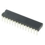
| 描述 | IC ADC 12BIT MONO 3OUT 28DIP模数转换器 - ADC IC 12-BIT |
| 产品分类 | |
| 品牌 | Analog Devices |
| 产品手册 | |
| 产品图片 |
|
| rohs | 符合RoHS无铅 / 符合限制有害物质指令(RoHS)规范要求 |
| 产品系列 | 数据转换器IC,模数转换器 - ADC,Analog Devices AD674BKNZ- |
| 数据手册 | |
| 产品型号 | AD674BKNZ |
| 产品种类 | 模数转换器 - ADC |
| 位数 | 12 |
| 供应商器件封装 | 28-PDIP |
| 分辨率 | 12 bit |
| 包装 | 管件 |
| 商标 | Analog Devices |
| 安装类型 | 通孔 |
| 安装风格 | Through Hole |
| 封装 | Tube |
| 封装/外壳 | 28-DIP(0.600",15.24mm) |
| 封装/箱体 | PDIP-28 |
| 工作温度 | 0°C ~ 70°C |
| 工作电源电压 | 5 V, 15 V |
| 工厂包装数量 | 13 |
| 接口类型 | Parallel |
| 数据接口 | 并联 |
| 最大功率耗散 | 375 mW |
| 最大工作温度 | + 125 C |
| 最小工作温度 | - 55 C |
| 标准包装 | 13 |
| 特性 | - |
| 电压参考 | Internal |
| 电压源 | 双 ± |
| 系列 | AD674B |
| 结构 | SAR |
| 转换器数 | 1 |
| 转换器数量 | 1 |
| 转换速率 | 66 kS/s |
| 输入数和类型 | 2 个单端,单极2 个单端,双极 |
| 输入类型 | Single-Ended |
| 通道数量 | 1 Channel |
| 采样率(每秒) | 66k |


- 商务部:美国ITC正式对集成电路等产品启动337调查
- 曝三星4nm工艺存在良率问题 高通将骁龙8 Gen1或转产台积电
- 太阳诱电将投资9.5亿元在常州建新厂生产MLCC 预计2023年完工
- 英特尔发布欧洲新工厂建设计划 深化IDM 2.0 战略
- 台积电先进制程称霸业界 有大客户加持明年业绩稳了
- 达到5530亿美元!SIA预计今年全球半导体销售额将创下新高
- 英特尔拟将自动驾驶子公司Mobileye上市 估值或超500亿美元
- 三星加码芯片和SET,合并消费电子和移动部门,撤换高东真等 CEO
- 三星电子宣布重大人事变动 还合并消费电子和移动部门
- 海关总署:前11个月进口集成电路产品价值2.52万亿元 增长14.8%


PDF Datasheet 数据手册内容提取
a Complete 12-Bit A/D Converters AD674B /AD774B FEATURES FUNCTIONAL BLOCK DIAGRAM Complete Monolithic 12-Bit A/D Converters with Reference, Clock, and Three-State Output Buffers Industry Standard Pinout 5V SUPPLY STATUS VLOGIC 1 28 STS H88 -i(cid:2) gashn (dSM p1ae6xe-B)d Ci tUo Mpngvicrerarodspieorson fc oTerism sAoeDr ( 5IA7nD4teA7r7f4aBce) DATAB YMTCOEHD AIEPD SSDEERLLE1EES2CCCS/S8TT/ 23 CONTROL M3SBNBBY 2276 DDBB1110 (MSB) 15 (cid:2)s (Max) Conversion Time (AD674B) SHORT CYCLE A 0 4 ST EL 25 DB9 (cid:3)CMo5IRLm Va-Smn, Tg(cid:3)eDer1 c-G08ia 8rVla3,, d- IC0ne osdVmu–s1pt0lri iaVanl,, t 0 aV nVed–r 2sMi0o iVlnits aI nArpyv uaTtie lRambaplneegreasture REAAN1D1A0/2CVLVCOO R/H1GNE5IPV FVCR EE EOSERRNUMFTEAP MONBRVPOCCAUCL/LCNCEYCEET 56789 R10EVF CLOCK–+COMPSAI RDAC 12 OAUUEPTTT ANBBBYEL 2222243210 DDDDDBBBBB87654 DDOAIUGTTAITPAULTS REFERENCE RINEPFU INT 10 I REF BU NY 19 DB3 –B1I12P0VOV/–L S1A5PRVA NOSB FUIIN1PFP0POSVPVUEFELIYNTFTE 111123 19k9(cid:1).95 +–DAC N VEE RESFFLSBBBCEL 111876 DDDBBB021 (LSB) 20V SPAN INPUT DIGITAL 20VIN 14 VDOIVLTIDAEGRE AD674B/AD774B 15 COMMON DC PRODUCT DESCRIPTION PRODUCT HIGHLIGHTS The AD674B and AD774B are complete 12-bit successive- 1. Industry Standard Pinout: The AD674B and AD774B use approximation analog-to-digital converters with three-state the pinout established by the industry standard AD574A. output buffer circuitry for direct interface to 8- and 16-bit 2. Analog Operation: The precision, laser-trimmed scaling and microprocessor busses. A high-precision voltage reference and bipolar offset resistors provide four calibrated ranges: 0 V to clock are included on chip, and the circuit requires only power 10 V and 0 V to 20 V unipolar; –5 V to +5 V and –10 V to supplies and control signals for operation. +10 V bipolar. The AD674B and AD774B operate on +5 V The AD674B and AD774B are pin-compatible with the indus- and ±12 V or ±15 V power supplies. try standard AD574A, but offer faster conversion time and bus- 3. Flexible Digital Interface: On-chip multiple-mode three-state access speed than the AD574A and lower power consumption. output buffers and interface logic allow direct connection to The AD674B converts in 15 µs (maximum) and the AD774B most microprocessors. The 12 bits of output data can be converts in 8 µs (maximum). read either as one 12-bit word or as two 8-bit bytes (one with The monolithic design is implemented using Analog Devices’ 8 data bits, the other with 4 data bits and 4 trailing zeros). BiMOS II process allowing high-performance bipolar analog 4. The internal reference is trimmed to 10.00 V with 1% maxi- circuitry to be combined on the same die with digital CMOS logic. mum error and 10 ppm/°C typical temperature coefficient. Offset, linearity, and scaling errors are minimized by active The reference is available externally and can drive up to laser trimming of thin-film resistors. 2.0 mA beyond the requirements of the converter and bipo- Five different grades are available. The J and K grades are lar offset resistors. specified for operation over the 0°C to 70°C temperature range. 5. The AD674B and AD774B are available in versions compli- The A and B grades are specified from –40°C to +85°C, the T grade ant with MIL-STD-883. Refer to the Analog Devices Mili- is specified from –55°C to +125°C. The J and K grades are tary Products Databook or current AD674B/AD774B/883B available in a 28-lead plastic DIP or 28-lead SOIC. All other grades data sheet for detailed specifications. are available in a 28-lead hermetically sealed ceramic DIP. REV.C Information furnished by Analog Devices is believed to be accurate and reliable. However, no responsibility is assumed by Analog Devices for its use, nor for any infringements of patents or other rights of third parties that One Technology Way, P.O. Box 9106, Norwood, MA 02062-9106, U.S.A. may result from its use. No license is granted by implication or otherwise Tel: 781/329-4700 www.analog.com under any patent or patent rights of Analog Devices. Fax: 781/326-8703 © Analog Devices, Inc., 2002
AD674B/AD774B–SPECIFICATIONS (T to T with V = +15 V (cid:3) 10% or +12 V (cid:3) 5%, MIN MAX CC V = +5 V (cid:3) 10%, V = –15 V (cid:3) 10% or –12 V (cid:3) 5%, unless otherwise noted.) LOGIC EE J Grade K Grade A Grade B Grade T Grade Model (AD674B or AD774B) Min Typ Max Min Typ Max Min Typ Max Min Typ Max Min Typ Max Unit RESOLUTION 12 12 12 12 12 Bits LINEARITY ERROR @ 25°C (cid:3)1 (cid:3)1/2 (cid:3)1 (cid:3)1/2 (cid:3)1/2 LSB T to T (cid:3)1 (cid:3)1/2 (cid:3)1 (cid:3)1/2 (cid:3)1 LSB MIN MAX DIFFERENTIAL LINEARITY ERROR (Minimum Resolution for Which No Missing Codes are Guaranteed) 12 12 12 12 12 Bits UNIPOLAR OFFSET1 @ 25°C (cid:3)2 (cid:3)2 (cid:3)2 (cid:3)2 (cid:3)2 LSB BIPOLAR OFFSET1 @ 25°C (cid:3)6 (cid:3)3 (cid:3)6 (cid:3)3 (cid:3)3 LSB FULL-SCALE CALIBRATION ERROR1, 2 @ 25°C (with Fixed 50 Ω Resistor from REF OUT to REF IN) 0.1 0.25 0.1 0.125 0.1 0.25 0.1 0.125 0.1 0.125 % of FS TEMPERATURE RANGE 0 70 0 70 –40 +85 –40 +85 –55 +125 °C TEMPERATURE DRIFT3 (Using Internal Reference) Unipolar (cid:3)2 (cid:3)1 (cid:3)2 (cid:3)1 (cid:3)1 LSB Bipolar Offset (cid:3)2 (cid:3)1 (cid:3)2 (cid:3)1 (cid:3)2 LSB Full-Scale Calibration (cid:3)6 (cid:3)2 (cid:3)8 (cid:3)5 (cid:3)7 LSB POWER SUPPLY REJECTION Max Change in Full-Scale Calibration V = +15 V ± 1.5 V or +12 V ± 0.6 V (cid:3)2 (cid:3)1 (cid:3)2 (cid:3)1 (cid:3)1 LSB CC V = +5 V ± 0.5 V (cid:3)1/2 (cid:3)1/2 (cid:3)1/2 (cid:3)1/2 (cid:3)1/2 LSB LOGIC V = –15 V ± 1.5 V or –12 V ± 0.6 V (cid:3)2 (cid:3)1 (cid:3)2 (cid:3)1 (cid:3)1 LSB EE ANALOG INPUT Input Ranges Bipolar –5 +5 –5 +5 –5 +5 –5 +5 –5 +5 V –10 +10 –10 +10 –10 +10 –10 +10 –10 +10 V Unipolar 0 10 0 10 0 10 0 10 0 10 V 0 20 0 20 0 20 0 20 0 20 V Input Impedance 10 V Span 3 5 7 3 5 7 3 5 7 3 5 7 3 5 7 kΩ 20 V Span 6 10 14 6 10 14 6 10 14 6 10 14 6 10 14 kΩ POWER SUPPLIES Operating Range V 4.5 5.5 4.5 5.5 4.5 5.5 4.5 5.5 4.5 5.5 V LOGIC V 11.4 16.5 11.4 16.5 11.4 16.5 11.4 16.5 11.4 16.5 V CC V –16.5 –11.4 –16.5 –11.4 –16.5 –11.4 –16.5 –11.4 –16.5 –11.4 V EE Operating Current I 3.5 7 3.5 7 3.5 7 3.5 7 3.5 7 mA LOGIC I 3.5 7 3.5 7 3.5 7 3.5 7 3.5 7 mA CC I 10 14 10 14 10 14 10 14 10 14 mA EE POWER CONSUMPTION 220 375 220 375 220 375 220 375 220 375 mW4 175 175 175 175 175 mW5 INTERNAL REFERENCE VOLTAGE 9.9 10.0 10.1 9.9 10.0 10.1 9.9 10.0 10.1 9.9 10.0 10.1 9.9 10.010.1 V Output Current (Available for External Loads) 2.0 2.0 2.0 2.0 2.0 mA (External Load Should Not Change During the Conversion) NOTES 1Adjustable to zero. 2Includes internal voltage reference error. 3Maximum change from 25°C value to the value at TMIN or TMAX. 4Tested with REF OUT tied to REF IN through 50 Ω resistor, VCC = +16.5 V, VEE = –16.5 V, VLOGIC = +5.5 V, and outputs in high-Z mode. 5Tested with REF OUT tied to REF IN through 50 Ω resistor, VCC = +12 V, VEE = –12 V, VLOGIC = +5 V, and outputs in high-Z mode. Specifications subject to change without notice. Specifications shown in boldface are tested on all devices at final electrical test at TMIN, 25°C, and TMAX. Results from those tests are used to calculate outgoing quality levels. All min and max specifications are guaranteed, although only those shown in boldface are tested. –2– REV. C
AD674B/AD774B (For all grades T to T with V = +15 V (cid:3) 10% or +12 V (cid:3) 5%, V = +5 V (cid:3) 10%, DIGITAL SPECIFICATIONS MIN MAX CC LOGIC V = –15 V (cid:3) 10% or –12 V (cid:3) 5%, unless otherwise noted.) EE Parameter Test Conditions Min Max Unit LOGIC INPUTS V High Level Input Voltage 2.0 V + 0.5 V IH LOGIC V Low Level Input Voltage –0.5 +0.8 V IL I High Level Input Current V = V –10 +10 µA IH IN LOGIC I Low Level Input Current V = 0 V –10 +10 µA IL IN C Input Capacitance 10 pF IN LOGIC OUTPUTS V High Level Output Voltage I = 0.5 mA 2.4 V OH OH V Low Level Output Voltage I = 1.6 mA 0.4 V OL OL I High-Z Leakage Current V = 0 to V –10 +10 µA OZ IN LOGIC C High-Z Output Capacitance 10 pF OZ (For all grades T to T with V = +15 V (cid:3) 10% or +12 V (cid:3) 5%, SWITCHING SPECIFICATIONS MIN MAX CC V = +5 V (cid:3) 10%, V = –15 V (cid:3) 10% or –12 V (cid:3) 5%, unless otherwise noted.) LOGIC EE CONVERTER START TIMING (Figure 1) CE tHEC t J, K, A, B Grades T Grade t HSC CS SSC Parameter Symbol Min Typ Max Min Typ Max Unit t t SRC HRC Conversion Time R/C 8-Bit Cycle (AD674B) t 6 8 10 6 8 10 µs C 12-Bit Cycle (AD674B) t 9 12 15 9 12 15 µs C 8-Bit Cycle (AD774B) tC 4 5 6 4 5 6 µs A0 tHAC 12-Bit Cycle (AD774B) tC 6 7.3 8 6 7.3 8 µs tSAC STS Delay from CE t 200 225 ns DSC STS CE Pulsewidth t 50 50 ns HEC tC CCSS tLoo Cw ED Suertinugp CE High ttSSC 5500 5500 nnss DB11 – DB0 tDSC HIGH HSC IMPEDANCE R/C to CE Setup t 50 50 ns SRC Figure 1. Convert Start Timing R/C LOW During CE High t 50 50 ns HRC A to CE Setup t 0 0 ns 0 SAC CE A Valid During CE High t 50 50 ns 0 HAC t t HSR SSR CS READ TIMING—FULL CONTROL MODE (Figure 2) R/C tSRR tHRR J, K, A, B Grades T Grade Parameter Symbol Min Typ Max Min Typ Max Unit A0 tSAR tHAR Access Time DatCa LV =al i1d0 A0 fpteFr CE Low ttDD1 252 75 150 252 75 150 nnss STS tHD HD 203 154 ns DB11 – DB0 HIGH DATA HIGH Output Float Delay tHL5 150 150 ns IMPEDANCE tDD VALID tHL IMPEDANCE CS to CE Setup t 50 50 ns SSR Figure 2. Read Cycle Timing R/C to CE Setup t 0 0 ns SRR A to CE Setup t 50 50 ns 5V 0 SAR CS Valid After CE Low tHSR 0 0 ns 3k(cid:1) R/C High After CE Low tHRR 0 0 ns DBN DBN A0 Valid After CE Low tHAR 50 50 ns 3k(cid:1) 100pF 100pF NOTES 1t is measured with the load circuit of Figure 3a and is defined as the time required HIGH-Z TO LOGIC 1 HIGH-Z TO LOGIC 0 DD for an output to cross 0.4 V or 2.4 V. High-Z to Logic 1 High-Z to Logic 0 20°C to T . MAX Figure 3a. Load Circuit for Access Time Test 3At –40°C. 4At –55°C. 5V 5t is defined as the time required for the data lines to change 0.5 V when loaded with HL 3k(cid:1) the circuit of Figure 3b. DBN DBN Specifications shown in boldface are tested on all devices at final electrical test with 3k(cid:1) 100pF 100pF worst case supply voltages at T , 25°C, and T . Results from those tests are used MIN MAX to calculate outgoing quality levels. All min and max specifications are guaranteed, LOGIC 1 TO HIGH-Z LOGIC 0 TO HIGH-Z although only those shown in boldface are tested. Specifications subject to change without notice. Logic 1 to High-Z Logic 0 to High-Z Figure 3b. Load Circuit for Output Float Delay Test REV. C –3–
AD674B/AD774B TIMING—STAND ALONE MODE (Figures 4a and 4b) t HRL J, K, A, B Grades T Grade R/C Parameter Symbol Min Typ Max Min Typ Max Unit Data Access Time tDDR 150 150 ns tDS Low R/C Pulsewidth t 50 50 ns HRL STS Delay from R/C t 200 225 ns DS STS Data Valid After R/C Low t 25 25 ns STS Delay After Data ValidtHDR 30 200 600 30 200 600 ns tC HS High R/C Pulsewidth tHRH 150 150 ns tHDR tHS Specifications subject to change without notice. DB11–DB0 VDAALTIAD HIGH–Z DATA VALID ABSOLUTE MAXIMUM RATINGS* Flgure 4a. Standalone Mode Timing Low Pulse R/C V to Digital Common . . . . . . . . . . . . . . . . . . . 0 to +16.5 V CC V to Digital Common . . . . . . . . . . . . . . . . . . . . 0 to –16.5 V EE V to Digital Common . . . . . . . . . . . . . . . . . . . 0 to +7 V LOGIC Analog Common to Digital Common . . . . . . . . . . . . . . . ±1 V R/C Digital Inputs to Digital Common . . . –0.5 V to V +0.5 V LOGIC Analog Inputs to Analog Common . . . . . . . . . . . . V to V EE CC t t 20 V to Analog Common . . . . . . . . . . . . . . . . . . . . . . ±24 V HRH DS IN REF OUT . . . . . . . . . . . . . . . . . . Indefinite Short to Common STS . . . . . . . . . . . . . . . . . . . . . . . . . . . . .Momentary Short to VCC tC Junction Temperature . . . . . . . . . . . . . . . . . . . . . . . . . . 175°C t t DDR HDR Power Dissipation . . . . . . . . . . . . . . . . . . . . . . . . . . . 825 mW Lead Temperature, Soldering (10 sec) . . . . . . . . . . . . . 300°C Storage Temperature . . . . . . . . . . . . . . . . . . –65°C to +150°C DB11–DB0 HIGH–Z VDAALTIAD HIGH–Z t *Stresses above those listed under Absolute Maximum Ratings may cause perma- HL nent damage to the device. This is a stress rating only and functional operation of Figure 4b. Standalone Mode Timing High Pulse for R/C the device at these or any other conditions above those indicated in the operational section of this specification is not implied. Exposure to absolute maximum rating conditions for extended periods may affect device reliability. ORDERING GUIDE Conversion INL Package Package Modell Temperature Time (max) (T to T ) Description Option2 MIN MAX AD674BJN 0°C to 70°C 15 µs ±1 LSB Plastic DIP N-28 AD674BKN 0°C to 70°C 15 µs ±1/2 LSB Plastic DIP N-28 AD674BAR –40°C to +85°C 15 µs ±1 LSB Plastic SOIC R-28 AD674BBR –40°C to +85°C 15 µs ±1/2 LSB Plastic SOIC R-28 AD674BAD –40°C to +85°C 15 µs ±1 LSB Ceramic DIP D-28 AD674BBD –40°C to +85°C 15 µs ±1/2 LSB Ceramic DIP D-28 AD674BTD –55°C to +125°C 15 µs ±1 LSB Ceramic DIP D-28 AD774BJN 0°C to 70°C 8 µs ±1 LSB Plastic DIP N-28 AD774BKN 0°C to 70°C 8 µs ±1/2 LSB Plastic DIP N-28 AD774BAR –40°C to +85°C 8 µs ±1 LSB Plastic SOIC R-28 AD774BBR –40°C to +85°C 8 µs ±1/2 LSB Plastic SOIC R-28 AD774BAD –40°C to +85°C 8 µs ±1 LSB Ceramic DIP D-28 AD774BBD –40°C to +85°C 8 µs ±1/2 LSB Ceramic DIP D-28 AD774BTD –55°C to +125°C 8 µs ±1 LSB Ceramic DIP D-28 NOTES 1For details on grade and package offerings screened in accordance with MIL-STD-883, refer to the Analog Devices Military Products Databook or the current AD674B/ AD774B/883B data sheet. 2N = Plastic DIP; D = Hermetic DIP; R = Plastic SOIC. CAUTION ESD (electrostatic discharge) sensitive device. Electrostatic charges as high as 4000V readily WARNING! accumulate on the human body and test equipment and can discharge without detection. Although the AD674B/AD774B features proprietary ESD protection circuitry, permanent damage may occur on devices subjected to high energy electrostatic discharges. Therefore, proper ESD precautions are recommended to avoid performance degradation or loss of functionality. ESD SENSITIVE DEVICE –4– REV. C
AD674B/AD774B DEFINITION OF SPECIFICATIONS Quantization Uncertainty Linearity Error Analog-to-digital converters exhibit an inherent quantization Linearity error refers to the deviation of each individual code uncertainty of ±1/2 LSB. This uncertainty is a fundamental from a line drawn from “zero” through “full scale.” The point characteristic of the quantization process and cannot be reduced used as “zero” occurs 1/2 LSB (1.22 mV for 10 V span) before for a converter of given resolution. the first code transition (all zeroes to only the LSB “on”). “Full Left-Justified Data scale” is defined as a level 1 1/2 LSB beyond the last code tran- The output data format is left-justified. This means that the sition (to all ones). The deviation of a code from the true straight data represents the analog input as a fraction of full scale, rang- line is measured from the middle of each particular code. ing from 0 to 4095/4096. This implies a binary point 4095 to The K, B, and T grades are guaranteed for maximum nonlinear- the left of the MSB. ity of ±1/2 LSB. For these grades, this means that an analog Full-Scale Calibration Error value that falls exactly in the center of a given code width will The last transition (from 1111 1111 1110 to 1111 1111 1111) result in the correct digital output code. Values nearer the upper should occur for an analog value 1 1/2 LSB below the nominal or lower transition of the code width may produce the next upper full scale (9.9963 V for 10.000 V full scale). The full-scale cali- or lower digital output code. The J and A grades are guaranteed bration error is the deviation of the actual level at the last transi- to ±1 LSB max error. For these grades, an analog value that tion from the ideal level. This error, which is typically 0.05% to falls within a given code width will result in either the correct 0.1% of full scale, can be trimmed out as shown in Figures 7 code for that region or either adjacent one. and 8. The full-scale calibration error over temperature is given Note that the linearity error is not user adjustable. with and without the initial error trimmed out. The temperature coefficients for each grade indicate the maximum change in the Differential Linearity Error (No Missing Codes) full-scale gain from the initial value using the internal 10 V A specification that guarantees no missing codes requires that reference. every code combination appear in a monotonic increasing sequence as the analog input level is increased. Thus every code must have a Temperature Drift finite width. The AD674B and AD774B guarantee no missing codes The temperature drift for full-scale calibration, unipolar offset, to 12-bit resolution, requiring that all 4096 codes must be present and bipolar offset specifies the maximum change from the initial over the entire operating temperature ranges. (25°C) value to the value at T or T . MIN MAX Unipolar Offset Power Supply Rejection The first transition should occur at a level 1/2 LSB above analog The standard specifications assume use of +5.00 V and ±15.00 V common. Unipolar offset is defined as the deviation of the actual or ±12.00 V supplies. The only effect of power supply error on transition from that point. This offset can be adjusted as discussed the performance of the device will be a small change in the later. The unipolar offset temperature coefficient specifies the full-scale calibration. This will result in a linear change in all maximum change of the transition point over temperature, low-order codes. The specifications show the maximum full- with or without external adjustment. scale change from the initial value with the supplies at the various limits. Bipolar Offset In the bipolar mode the major carry transition (0111 1111 1111 Code Width to 1000 0000 0000) should occur for an analog value 1/2 LSB A fundamental quantity for A/D converter specifications is the below analog common. The bipolar offset error and temperature code width. This is defined as the range of analog input values for coefficient specify the initial deviation and maximum change in which a given digital output code will occur. The nominal value the error over temperature. of a code width is equivalent to 1 least significant bit (LSB) of the full-scale range or 2.44 mV out of 10 V for a 12-bit ADC. REV. C –5–
AD674B/AD774B PIN CONFIGURATION VLOGIC 1 28 STS 12/8 2 27 DB11 (MSB) CS 3 26 DB10 A0 4 25 DB9 AD674B R/C 5 OR 24 DB8 CE 6 AD774B 23 DB7 VCC 7 TOP VIEW 22 DB6 REF OUT 8 (Not to Scale) 21 DB5 AGND 9 20 DB4 REF IN 10 19 DB3 VEE 11 18 DB2 BIP OFF 12 17 DB1 10 VIN 13 16 DB0 (LSB) 20 VIN 14 15 DGND PIN FUNCTION DESCRIPTIONS Symbol Pin No. Type* Name and Function AGND 9 P Analog Ground (Common) A 4 DI Byte Address/Short Cycle. If a conversion is started with A Active LOW, a full 12-bit conversion 0 0 cycle is initiated. If A is Active HIGH during a convert start, a shorter 8-bit conversion cycle 0 results. During Read (R/C = 1) with 12/8 LOW, A = LOW enables the 8 most significant bits, 0 and A = HIGH enables DB3–DB0 and sets DB7–DB4 = 0. 0 BIP OFF 12 AI Bipolar Offset. Connect through a 50 Ω resistor to REF OUT for bipolar operation or to Analog Common for unipolar operation. CE 6 DI Chip Enable. Chip Enable is Active HIGH and is used to initiate a convert or read operation. CS 3 DI Chip Select. Chip Select is Active LOW. DB11–DB8 27–24 DO Data Bits 11 through 8. In the 12-bit format (see 12/8 and A pins) these pins provide the upper 0 4 bits of data. In the 8-bit format, they provide the upper 4 bits when A is LOW and are 0 disabled when A is HIGH. 0 DB7–DB4 23–20 DO Data Bits 7 through 4. In the 12-bit format these pins provide the middle 4 bits of data. In the 8-bit format they provide the middle 4 bits when A is LOW and all zeroes when A is HIGH. 0 0 DB3–DB0 19–16 DO Data Bits 3 through 0. In both the 12-bit and 8-bit format these pins provide the lower 4 bits of data when A is HIGH; they are disabled when A is LOW. 0 0 DGND 15 P Digital Ground (Common) REF OUT 8 AO 10 V Reference Output R/C 5 DI Read/Convert. In the full control mode R/C is Active HIGH for a read operation and Active LOW for a convert operation. In the standalone mode, the falling edge of R/C initiates a conversion. REF IN 10 AI Reference Input is connected through a 50 Ω resistor to +10 V Reference for normal operation. STS 28 DO Status is Active HIGH when a conversion is in progress and goes LOW when the conversion is completed. V 7 P +12 V/+15 V Analog Supply CC V 11 P –12 V/–15 V Analog Supply EE V 1 P 5 V Logic Supply LOGIC 10 V 13 AI 10 V Span Input, 0 V to +10 V unipolar mode or –5 V to +5 V bipolar mode. When using the IN 20 V Span, 10 V should not be connected. IN 20 V 14 AI 20 V Span Input, 0 V to +20 V unipolar mode or –10 V to +10 V bipolar mode. When using the IN 10 V Span, 20 V should not be connected. IN 12/8 2 DI The 12/8 pin determines whether the digital output data is to be organized as two 8-bit words (12/8 LOW) or a single 12-bit word (12/8 HIGH). *Types: AI = Analog Input, AO = Analog Output, DI = Digital Input, DO = Digital Output, P = Power –6– REV. C
AD674B/AD774B CIRCUIT OPERATION DRIVING THE ANALOG INPUT The AD674B and AD774B are complete 12-bit monolithic A/D The AD674B and AD774B are successive-approximation analog- converters that require no external components to provide the to-digital converters. During the conversion cycle, the ADC input complete successive-approximation analog-to-digital conversion current is modulated by the DAC test current at approximately function. A block diagram is shown in Figure 5. a 1 MHz rate. Thus it is important to recognize that the signal source driving the ADC must be capable of holding a constant output voltage under dynamically changing load conditions. 5V SUPPLY STATUS VLOGIC 1 28 STS DATA MODE SEL1E2C/8T 2 MSBN 27 DB11 (MSB) FEEDBACK TO AMPLIFIER CHIP SELECCST 3 CONTROL 3 BY 26 DB10 V+ BYTE ADDRESS/ B SHORT CYCLE A 0 4 ST EL 25 DB9 RERA–AEBN11DFI1221AP0/E00V2CVLOVVV/RCOO –L R/EHSS11GNAEN55IPPPVR FVVAACCR E E ENNEOOSSEBRRN R FUUMIFIIITENNNA1PEFPP M0ONPOPPBRSVFVPPVOCCAUUUUC ELFE/LLIICNNCEYYNCEETTFTTTE 1111567890123 19kR91(cid:1).0E9VF5 CLO+–DCAK–+IC RCEOFMPSNAI RDAVCEE12 OAUUBUREPESTTTFFLSBANBBBNBBCEEYYLL 222221111432109876 DDDDDDDDDDBBBBBBBBBIG087654321I T(ALSLB) DDOAIUGTTAITPAULTS RECLSUIIMRSRTITOEIANRNNGSTALOVG– COCAROIINMHMEP ISAEMPSPNNL OMOI-GFLONNEIOEDSSOREU IP N LPL A OUI TMTLUEEISTTSDEPET UBD LCTY OBU AIYMRDRPEENDAT.NCE. IDIFFRIN IITINEACSDTOCMPACORUUASDRTTAAROPCREURNTT 20VIN 14 VDOIVLTIDAEGRE AD674B/AD774B 15 COMMON DC Figure 6.Op Amp—ADC Interface Figure 5.Block Diagram of AD674B and AD774B The closed-loop output impedance of an op amp is equal to the When the control section is commanded to initiate a conversion open-loop output impedance (usually a few hundred ohms) (as described later) it enables the clock and resets the divided by the loop gain at the frequency of interest. It is often successive-approximation register (SAR) to all zeroes. Once a assumed that the loop gain of a follower-connected op amp is conversion cycle has begun, it cannot be stopped or restarted sufficiently high to reduce the closed-loop output impedance to and data is not available from the output buffers. The SAR, a negligibly small value, particularly if the signal is low fre- timed by the clock, will sequence through the conversion cycle quency. However, the amplifier driving the ADC must either and return an end-of-convert flag to the control section. The have sufficient loop gain at 1 MHz to reduce the closed-loop control section will then disable the clock, bring the output output impedance to a low value or have low open-loop output status flag low, and enable control functions to allow data read impedance. This can be accomplished by using a wideband op by external command. amp, such as the AD711. During the conversion cycle, the internal 12-bit current output If a sample-hold amplifier is required, the monolithic AD585 or DAC is sequenced by the SAR from the most significant bit AD781 is recommended, with the output buffer driving the (MSB) to least significant bit (LSB) to provide an output cur- AD674B or AD774B input directly. A better alternative is the rent that accurately balances the input signal current through AD1674, which is a 10 µs sampling ADC in the same pinout as the the divider network. The comparator determines whether the AD574A, AD674A, or AD774B and is functionally equivalent. addition of each successively weighted bit current causes the DAC current sum to be greater or less than the input current; if SUPPLY DECOUPLING AND LAYOUT the sum is less, the bit is left on; if more, the bit is turned off. CONSIDERATION After testing all the bits, the SAR contains a 12-bit binary code It is critical that the power supplies be filtered, well regulated, that accurately represents the input signal to within ±1/2 LSB. and free from high-frequency noise. Use of noisy supplies will cause unstable output codes. Switching power supplies is not The temperature-compensated reference provides the primary recommended for circuits attempting to achieve 12-bit accuracy voltage reference to the DAC and guarantees excellent stability unless great care is used in filtering any switching spikes present with both time and temperature. The reference is trimmed to in the output. Few millivolts of noise represent several counts of 10.00 V ± 1%; it can supply up to 2.0 mA to an external load in error in a 12-bit ADC. addition to the requirements of the reference input resistor (0.5 mA) and bipolar offset resistor (0.5 mA). Any external load Decoupling capacitors should be used on all power supply pins; on the reference must remain constant during conversion. The the 5 V supply decoupling capacitor should be connected directly thin-film application resistors are trimmed to match the full- from Pin 1 to Pin 15 (digital common) and the +VCC and –VEE scale output current of the DAC. The input divider network pins should be decoupled directly to analog common (Pin 9). A provides a 10 V or 20 V input range. The bipolar offset resistor suitable decoupling capacitor is a 4.7 µF tantalum type in paral- is grounded for unipolar operation and connected to the 10 V lel with a 0.1 µF ceramic disc type. reference for bipolar operation. REV. C –7–
AD674B/AD774B Circuit layout should attempt to locate the ADC, associated UNIPOLAR CALIBRATION analog input circuitry, and interconnections as far as possible The connections for unipolar ranges are shown in Figure 7. The from logic circuitry. For this reason, the use of wire-wrap circuit AD674B or AD774B is trimmed to a nominal 1/2 LSB offset so construction is not recommended. Careful printed-circuit layout that the exact analog input for a given code will be in the middle and manufacturing is preferred. of that code (halfway between the transitions to the codes above and below it). Thus, when properly calibrated, the first transition UNIPOLAR RANGE CONNECTIONS FOR THE AD674B (from 0000 0000 0000 to 0000 0000 0001) will occur for an input AND AD774B level of +1/2 LSB (1.22 mV for 10 V range). The AD674B and AD774B contain all the active components If Pin 12 is connected to Pin 9, the unit will behave in this manner, required to perform a complete 12-bit A/D conversion. Thus, within specifications. If the offset trim (R1) is used, it should be for most situations, all that is necessary is connection of the trimmed as above, although a different offset can be set for a power supplies (+5 V, +12/+15 V, and –12/–15 V), the analog particular system requirement. This circuit will give approximately input, and the conversion initiation command, as discussed on ±15 mV of offset trim range. the next page. The full-scale trim is done by applying a signal 1 1/2 LSB below the nominal full scale (9.9963 for a 10 V range). Trim R2 to AD674B/AD774B OFFSET give the last transition (1111 1111 1110 to 1111 1111 1111). R1 2 12/8 STS 28 –12V/ 100k(cid:1) +12V/ 3 CS –15V +15V 4 A0 HIGH2 B4–IT2S7 BIPOLAR OPERATION GAIN 5 R/C The connections for bipolar ranges are shown in Figure 8. 6 CE MIDDLE BITS Again, as for the unipolar ranges, if the offset and gain specifica- 100k(cid:1) R2 20–23 100(cid:1) 10 REF IN LOW BITS tions are sufficient, one or both of the trimmers shown can be 8 REF OUT 16–19 replaced by a 50 Ω ±1% fixed resistor. The analog input is 100(cid:1) 12 BIP OFF applied as for the unipolar ranges. Bipolar calibration is similar 0 TO 10V +5V 1 to unipolar calibration. First, a signal 1/2 LSB above negative ANALOG 13 10VIN +15V 7 full scale (–4.9988 V for the ±5 V range) is applied and R1 is INPUTS 14 20VIN –15V 11 trimmed to give the first transition (0000 0000 0000 to 0000 0 TO 20V 9 ANA COM DIG COM 15 0000 0001). Then a signal 1 1/2 LSB below positive full scale (+4.9963 V for the ±5 V range) is applied and R2 trimmed to give the last transition (1111 1111 1110 to 1111 1111 1111). Figure 7.Unipolar Input Connections All of the thin-film application resistors of the AD674B and AD674B/AD774B AD774B are factory trimmed for absolute calibration. Therefore, 2 12/8 STS 28 in many applications, no calibration trimming will be required. 3 CS The absolute accuracy for each grade is given in the specification 4 A0 HIGH2 B4–IT2S7 5 R/C tables. For example, if no trims are used, ±2 LSB max zero offset 6 CE MIDDLE BITS error and ±0.25% (10 LSB) max full-scale error are guaranteed. GAIN R2 10 REF IN 20–23 100(cid:1) If the offset trim is not required, Pin 12 can be connected directly 8 REF OUT LOW BITS to Pin 9; the two resistors and trimmer for Pin 12 are then not 100(cid:1) 16–19 OFFSET 12 BIP OFF needed. If the full-scale trim is not required, a 50 Ω 1% metal R1 +5V 1 film resistor should be connected between Pin 8 and Pin 10. (cid:3)5V ANALOG 13 10VIN +15V 7 The analog input is connected between Pins 13 and 9 for a 0 V INPUTS(cid:3)10V 14 20VIN –15V 11 to 10 V input range, between Pins 14 and 9 for a 0 V to 20 V 9 ANA COM DIG COM 15 input range. Input signals beyond the supplies are easily accommo- dated. For the 10 V span input, the LSB has a nominal value of Figure 8.Bipolar Input Connections 2.44 mV; for the 20 V span, 4.88 mV. If a 10.24 V range is desired (nominal 2.5 mV/bit), the gain trimmer (R2) should be GROUNDING CONSIDERATIONS replaced by a 50 Ω resistor and a 200 Ω trimmer inserted in The analog common at Pin 9 is the ground reference point for series with the analog input to Pin 13 (for a full-scale range of the internal reference and is thus the “high quality” ground for 20.48 V [5 mV/bit] use a 500 Ω trimmer into Pin 14). The the ADC; it should be connected directly to the analog reference gain trim described below is now done with these trimmers. point of the system. To achieve the high-accuracy performance The nominal input impedance into Pin 13 is 5 kΩ, and into Pin available from the ADC in an environment of high digital noise 14 is 10kΩ. content, the analog and digital commons must be connected together at the package. In some situations, the digital common at Pin 15 can be connected to the most convenient ground ref- erence point; digital power return is preferred. –8– REV. C
AD674B/AD774B VALUE OF A0 AT LAST CONVERT COMMAND Q D D EOC 12 EN EN EOC 8 START CONVERT R Q SAR S S Q RESET R QB CE HIGH IF CONVERSION IN PROGRESS CS CLK EN R/C STATUS NYBBLE A A0 ENABLE NYBBLE B READ ENABLE TO OUTPUT NYBBLE C BUFFERS ENABLE 12/8 NYBBLE = 0 ENABLE Figure 9.Equivalent Internal Logic Circuitry CONTROL LOGIC Table I. Truth Table The AD674B and AD774B contain on-chip logic to provide conversion initiation and data read operations from signals CE CS R/C 12/8 A0 Operation commonly available in microprocessor systems; this internal 0 X X X X None logic circuitry is shown in Figure 9. X 1 X X X None The control signals CE, CS, and R/C control the operation of 1 0 0 X 0 Initiate 12-Bit Conversion the converter. The state of R/C when CE and CS are both 1 0 0 X 1 Initiate 8-Bit Conversion asserted determines whether a data read (R/C = 1) or a convert 1 0 1 1 X Enable 12-Bit Parallel Output (R/C = 0) is in progress. The register control inputs, A and 1 0 1 0 0 Enable 8 Most Significant Bits 0 12/8, control conversion length and data format. If a conversion 1 0 1 0 1 Enable 4 LSBs + 4 Trailing Zeroes is started with A low, a full 12-bit conversion cycle is initiated. 0 If A is high during a convert start, a shorter 8-bit conversion The ADC may be operated in one of two modes, the full-control 0 cycle results. During data read operations, A determines mode and the standalone mode. The full-control mode uses all 0 whether the three-state buffers containing the 8 MSBs of the the control signals and is useful in systems that address decode conversion result (A = 0) or the 4 LSBs (A = 1) are enabled. multiple devices on a single data bus. The standalone mode is 0 0 The 12/8 pin determines whether the output data is to be orga- useful in systems with dedicated input ports available. In gen- nized as two 8-bit words (12/8 tied to DIGITAL COMMON) eral, the standalone mode is capable of issuing start-convert or a single 12-bit word (12/8 tied to V ). In the 8-bit mode, commands on a more precise basis and therefore produces LOGIC the byte addressed when A is high contains the 4 LSBs from higher accuracy results. The following sections describe these 0 the conversion followed by four trailing zeroes. This organiza- two modes in more detail. tion allows the data lines to be overlapped for direct interface to 8-bit buses without the need for external three-state buffers. FULL-CONTROL MODE Chip Enable (CE), Chip Select (CS), and Read/Convert (R/C) An output signal, STS, indicates the status of the converter. are used to control Convert or Read modes of operation. Either STS goes high at the beginning of a conversion and returns low CE or CS may be used to initiate a conversion. The state of R/C when the conversion cycle is complete. when CE and CS are both asserted determines whether a data Read (R/C = 1) or a Convert (R/C = 0) is in progress. R/C should be LOW before both CE and CS are asserted; if R/C is HIGH, a Read operation will momentarily occur, possibly resulting in system bus contention. REV. C –9–
AD674B/AD774B STANDALONE MODE GENERAL A/D CONVERTER INTERFACE “Standalone” mode is useful in systems with dedicated input CONSIDERATIONS ports available and thus not requiring full bus interface capabil- A typical A/D converter interface routine involves several opera- ity. Standalone mode applications are generally able to issue tions. First, a write to the ADC address initiates a conversion. conversion start commands more precisely than full-control The processor must then wait for the conversion cycle to com- mode, resulting in improved accuracy. plete, since most integrated circuit ADCs take longer than one instruction cycle to complete a conversion. Valid data can, of CE and 12/8 are wired HIGH, CS and A are wired LOW, and 0 course, only be read after the conversion is complete. The conversion is controlled by R/C. The three-state buffers are AD674B and AD774B provide an output signal (STS) which enabled when R/C is HIGH and a conversion starts when R/C indicates when a conversion is in progress. This signal can be goes LOW. This gives rise to two possible control signals—a polled by the processor by reading it through an external three- high pulse or a low pulse. Operation with a low pulse is shown state buffer (or other input port). The STS signal can also in Figure 4a. In this case, the outputs are forced into the high generate an interrupt upon completion of conversion if the sys- impedance state in response to the falling edge of R/C and tem timing requirements are critical and the processor has other return to valid logic levels after the conversion cycle is completed. tasks to perform during the ADC conversion cycle. Another The STS line goes HIGH 200 ns after R/C goes LOW and possible time-out method is to assume that the ADC will take its returns low 600 ns after data is valid. maximum conversion time to convert, and insert a sufficient If conversion is initiated by a high pulse as shown in Figure 4b, number of “no-op” instructions to ensure that this amount of the data lines are enabled during the time when R/C is HIGH. processor time is consumed. The falling edge of R/C starts the next conversion, and the data Once conversion is complete, the data can be read. For convert- lines return to three-state (and remain three-state) until the next ers with more data bits than are available on the bus, a choice of high pulse of R/C. data formats is required, and multiple read operations are needed. The AD674B and AD774B include internal logic to CONVERSION TIMING permit direct interface to 8-bit and 16-bit data buses, selected Once a conversion is started, the STS line goes HIGH. Convert by the 12/8 input. In 16-bit bus applications (12/8 high) the start commands will be ignored until the conversion cycle is complete. The output data buffers can be enabled up to 1.2 µs data lines (DB11 through DB0) may be connected to either the 12 most significant or 12 least significant bits of the data bus. prior to STS going LOW. The STS line will return LOW at the The remaining 4 bits should be masked in software. The inter- end of the conversion cycle. face to an 8-bit data bus (12/8 low) is done in a left-justified for- The register control inputs, A0 and 12/8, control conversion mat. The even address (A0 low) contains the 8 MSBs (DB11 length and data format. If a conversion is started with A0 LOW, through DB4). The odd address (A0 high) contains the 4 LSBs a full 12-bit conversion cycle is initiated. If A0 is HIGH during a (DB3 through DB0) in the upper half of the byte, followed by convert start, a shorter 8-bit conversion cycle results. four trailing zeroes, thus eliminating bit masking instructions. During data read operations, A0 determines whether the three- It is not possible to rearrange the output data lines for right-jus- state buffers containing the 8 MSBs of the conversion result tified 8-bit bus interface. (A = 0) or the 4 LSBs (A = 1) are enabled. The 12/8 pin 0 0 determines whether the output data is to be organized as two D7 D0 8-bit words (12/8 tied LOW) or a single 12-bit word (12/8 tied XXX0 DB11 DB10 DB9 DB8 DB7 DB6 DB5 DB4 HIGH). In the 8-bit mode, the byte addressed when A is high (EVEN ADDR) (MSB) 0 contains the 4 LSBs from the conversion followed by four trail- XXX1 DB3 DB2 DB1 DB0 0 0 0 0 (ODD ADDR) (LSB) ing zeroes. This organization allows the data lines to be over- lapped for direct interface to 8-bit buses without the need for Figure 10.Data Format for 8-Bit Bus external three-state buffers. –10– REV. C
AD674B/AD774B OUTLINE DIMENSIONS Dimensions shown in inches and (mm). 28-Lead Ceramic DIP Package (D-28) 0.05 (1.27) 0.050 (12.83) 0.045 (1.14) 28 15 0.59 30o 0.08 (2.0) +– 0.01 (14.98) SEATING 0.125 MIN (3.17) 1 14 PLANE 0(2.0.1865) 11..4420 ((3365..0576)) 0.095 (2.41) 0.14(35. 6 +– 8 )0.02 0.050 0(0.0.21504 +– +– 0 0.0.0052) +– 0.010 0.01(70 . +–4 3 0).003 0.1 (2.54) 0.047 +– 0.007 (1.27) 0.6 (15.24) (1.19) 28-Lead Plastic DIP Package (N-28) 1.565 (39.70) 1.380 (35.10) 28 15 0.580 (14.73) 0.485 (12.32) 1 14 PIN 1 0.060 (1.52) 0.625 (15.87) 0.015 (0.38) 0.600 (15.24) 0.250 0.195 (4.95) (6.35) 0.125 (3.18) MAX 0.150 (3.81) MIN 0.200 (5.05) 0.015 (0.381) 0.125 (3.18) 00..002124 ((00..535586)) (02.1.5040) (01.0.7770) SPELAANTIENG 0.008 (0.204) BSC MAX 28-Lead Wide Body SOIC Package (R-28) 0.7125 (18.10) 0.6969 (17.70) 28 15 0.2992 (7.60) 0.2914 (7.40) 0.4193 (10.65) 1 14 0.3937 (10.00) PIN 1 0.1043 (2.65) 0.0291 (0.74) 0.0926 (2.35) 0.0098 (0.25)(cid:6) 45(cid:5) 8(cid:5) 00..00101480 ((00..3100)) 0(B.10.S52C070) 00..00119328 ((00..4395)) SPELAANTIENG 00..00102951 ((00..3223)) 0(cid:5) 00..00510507 ((10..2470)) REV. C –11–
AD674B/AD774B Revision History Location Page Data Sheet changed from REV. B to REV. C. Edits to ORDERING GUIDE . . . . . . . . . . . . . . . . . . . . . . . . . . . . . . . . . . . . . . . . . . . . . . . . . . . . . . . . . . . . . . . . . . . . . . . . . . . . . .5 Add 28-Lead Wide Body SOIC Package Drawing . . . . . . . . . . . . . . . . . . . . . . . . . . . . . . . . . . . . . . . . . . . . . . . . . . . . . . . . . . . . . . 12 C) 2( 0 4/ 0- 8- 0 8 0 0 C A. S. U. N D I E T N RI P –12– REV. C
Mouser Electronics Authorized Distributor Click to View Pricing, Inventory, Delivery & Lifecycle Information: A nalog Devices Inc.: AD774BBD AD674BAR AD674BBD AD774BARZ AD774BTD AD674BBR AD674BTD/883B AD774BAR 5962- 9169003MXA AD774BBRZ AD674BARZ AD774BKN AD674BBRZ 5962-9169003M3A AD774BTD/883B AD674BTE/883B AD674BTD AD674BAD AD674BJNZ AD774BJNZ AD674BKN AD774BJN AD674BKNZ AD774BKNZ