ICGOO在线商城 > 集成电路(IC) > 数据采集 - 模数转换器 > LTC2481IDD#PBF

 Datasheet下载
- 型号: LTC2481IDD#PBF
- 制造商: LINEAR TECHNOLOGY
- 库位|库存: xxxx|xxxx
- 要求:
| 数量阶梯 | 香港交货 | 国内含税 |
| +xxxx | $xxxx | ¥xxxx |
查看当月历史价格
查看今年历史价格
LTC2481IDD#PBF产品简介:
ICGOO电子元器件商城为您提供LTC2481IDD#PBF由LINEAR TECHNOLOGY设计生产,在icgoo商城现货销售,并且可以通过原厂、代理商等渠道进行代购。 LTC2481IDD#PBF价格参考。LINEAR TECHNOLOGYLTC2481IDD#PBF封装/规格:数据采集 - 模数转换器, 16 Bit Analog to Digital Converter 1 Input 1 Sigma-Delta 10-DFN (3x3)。您可以下载LTC2481IDD#PBF参考资料、Datasheet数据手册功能说明书,资料中有LTC2481IDD#PBF 详细功能的应用电路图电压和使用方法及教程。
LTC2481IDD#PBF 是 Linear Technology(现为 Analog Devices)生产的一款高精度、低功耗 24 位模数转换器 (ADC),属于数据采集系列。其应用场景主要包括以下领域:

 1. 工业自动化与控制
   - 用于工业传感器信号的精确采集,例如温度、压力、流量和液位传感器。
   - 在工业控制系统中实现高分辨率的数据采集,确保系统运行的稳定性和精确性。

 2. 医疗设备
   - 应用于便携式医疗设备,如血压计、血糖仪和心电图(ECG)设备。
   - 提供高精度的生物电信号采集能力,支持低功耗设计以延长电池寿命。

 3. 环境监测
   - 用于气象站、水质监测和空气质量检测设备中,采集环境参数(如温湿度、气体浓度等)。
   - 高分辨率和低噪声特性使其适合微弱信号的测量。

 4. 精密测量仪器
   - 在实验室或现场使用的精密测量仪器中,如数字万用表、数据记录仪等。
   - 支持多通道输入,能够同时采集多个信号源的数据。

 5. 汽车电子
   - 用于汽车传感器数据采集,例如胎压监测系统(TPMS)、悬架系统和发动机管理系统的信号处理。
   - 其低功耗特性非常适合电池供电的车载应用。

 6. 消费电子产品
   - 用于智能家居设备中的传感器数据采集,如智能秤、环境控制器等。
   - 提供高精度的用户交互体验,同时满足小型化和低功耗的设计需求。

 特点总结
LTC2481 的 ΔΣ 架构和内置 PGA(可编程增益放大器)使其能够直接处理小幅度信号,无需额外的信号调理电路。此外,其低功耗特性(工作电流仅为几百微安)使其非常适合电池供电的应用场景。这些特点使得 LTC2481 成为需要高精度、低功耗和小型化解决方案的理想选择。
| 参数 | 数值 |
| 产品目录 | 集成电路 (IC) |
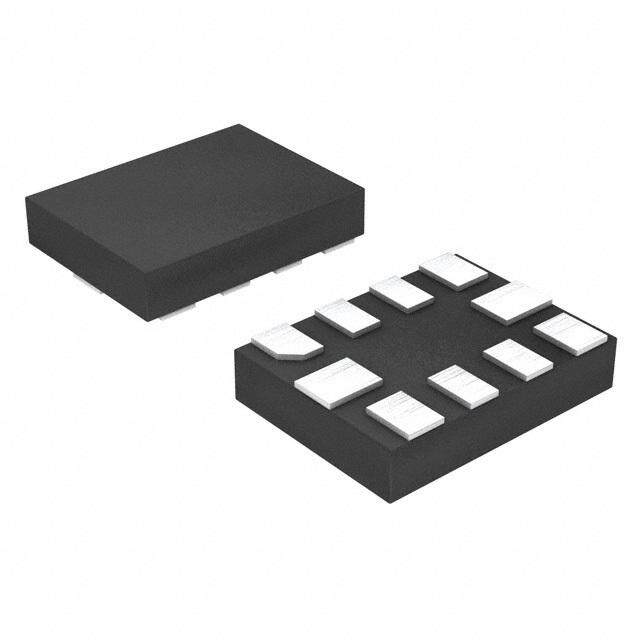
| 描述 | IC ADC 16BIT I2C 10-DFN |
| 产品分类 | |
| 品牌 | Linear Technology |
| 数据手册 | http://www.linear.com/docs/9657 |
| 产品图片 |
|
| 产品型号 | LTC2481IDD#PBF |
| rohs | 无铅 / 符合限制有害物质指令(RoHS)规范要求 |
| 产品系列 | - |
| 产品目录页面 | |
| 位数 | 16 |
| 供应商器件封装 | 10-DFN(3x3) |
| 其它名称 | LTC2481IDDPBF |
| 包装 | 管件 |
| 安装类型 | 表面贴装 |
| 封装/外壳 | 10-WFDFN 裸露焊盘 |
| 工作温度 | -40°C ~ 85°C |
| 数据接口 | I²C, 串行, SPI™ |
| 标准包装 | 121 |
| 电压源 | 单电源 |
| 转换器数 | 1 |
| 输入数和类型 | 2 个单端,双极1 个差分,双极 |
| 配用 | /product-detail/zh/DC951A/DC951A-ND/3029559 |
| 采样率(每秒) | 7.5 |


- 商务部:美国ITC正式对集成电路等产品启动337调查
- 曝三星4nm工艺存在良率问题 高通将骁龙8 Gen1或转产台积电
- 太阳诱电将投资9.5亿元在常州建新厂生产MLCC 预计2023年完工
- 英特尔发布欧洲新工厂建设计划 深化IDM 2.0 战略
- 台积电先进制程称霸业界 有大客户加持明年业绩稳了
- 达到5530亿美元!SIA预计今年全球半导体销售额将创下新高
- 英特尔拟将自动驾驶子公司Mobileye上市 估值或超500亿美元
- 三星加码芯片和SET,合并消费电子和移动部门,撤换高东真等 CEO
- 三星电子宣布重大人事变动 还合并消费电子和移动部门
- 海关总署:前11个月进口集成电路产品价值2.52万亿元 增长14.8%


PDF Datasheet 数据手册内容提取
LTC2481 16-Bit ∆Σ ADC with Easy Drive Input Current Cancellation 2 and I C Interface FeaTures DescripTion n Easy Drive™ Technology Enables Rail-to-Rail Inputs The LTC®2481 combines a 16-bit plus sign No Latency ∆Σ™ with Zero Differential Input Current analog-to-digital converter with patented Easy Drive n Directly Digitizes High Impedance Sensors with technology and I2C digital interface. The patented sampling Full Accuracy scheme eliminates dynamic input current errors and the n Programmable Gain from 1 to 256 shortcomings of on-chip buffering through automatic n GND to V Input/Reference Common Mode Range cancellation of differential input current. This allows large CC n 2-Wire I2C Interface external source impedances and input signals, with rail-to- n Programmable 50Hz, 60Hz or Simultaneous rail input range to be directly digitized while maintaining 50Hz/60Hz Rejection Mode exceptional DC accuracy. n 2ppm (0.25LSB) INL, No Missing Codes The LTC2481 includes on-chip programmable gain and n 1ppm Offset and 15ppm Full-Scale Error an oscillator. The LTC2481 can be configured through an n Selectable 2x Speed Mode I2C interface to provide a programmable gain from 1 to n No Latency: Digital Filter Settles in a Single Cycle 256 in 8 steps, to digitize an external signal or internal n Single Supply 2.7V to 5.5V Operation temperature sensor, reject line frequencies (50Hz, 60Hz or n Internal Oscillator simultaneous 50Hz/60Hz) as well as a 2x speed-up mode. n Six Addresses Available and One Global Address for Synchronization The LTC2481 allows a wide common mode input range n Available in a Tiny (3mm × 3mm) 10-Lead DFN Package (0V to VCC) independent of the reference voltage. The reference can be as low as 100mV or can be tied directly applicaTions to V . The LTC2481 includes an on-chip trimmed oscil- CC n Direct Sensor Digitizer lator eliminating the need for external crystals or oscil- n Weight Scales lators. Absolute accuracy and low drift are automatically n Direct Temperature Measurement maintained through continuous, transparent, offset and n Strain Gauge Transducers full-scale calibration. n Instrumentation L, LT, LTC, LTM, Linear Technology and the Linear logo are registered trademarks and n Industrial Process Control No Latency ∆∑ and Easy Drive are trademarks of Linear Technology Corporation. All other trademarks are the property of their respective owners. Patents Pending. n DVMs and Meters Typical applicaTion +FS Error vs R at IN+ and IN– SOURCE 80 VCC = 5V VCC 60 VVRINE+F == 35.V75V 0.1µF 1µF pm) 4200 VfTOAIN ==– G2=N5 1°D.C25V 10k IDIFF = 0 VIN+ REF+ VCC SSCDLA 2I2-CW IINRTEERFACE ROR (p 0 CIN = 1µF R SENSE LTC2481 CA0/f0 S E –20 10k VIN– GND REF– CA1 6 ADDRESSES +F –40 0.1µF 2481 TA01a –60 –80 1 10 100 1k 10k 100k RSOURCE (Ω) 2481 TA01b 2481fd 1 For more information www.linear.com/LTC2481
LTC2481 absoluTe MaxiMuM raTings pin conFiguraTion (Notes 1, 2) Supply Voltage (V ) to GND ...................... –0.3V to 6V TOP VIEW CC Analog Input Voltage to GND ....... –0.3V to (VCC + 0.3V) REF+ 1 10 CA0/f0 Reference Input Voltage to GND .. –0.3V to (VCC + 0.3V) VCC 2 9 CA1 Digital Input Voltage to GND ....... –0.3V to (VCC + 0.3V) REF – 3 11 8 GND IN+ 4 7 SDA Digital Output Voltage to GND ...... –0.3V to (V + 0.3V) CC IN– 5 6 SCL Operating Temperature Range LTC2481C .................................................... 0°C to 70°C DD PACKAGE 10-LEAD (3mm × 3mm) PLASTIC DFN LTC2481I .................................................–40°C to 85°C TJMAX = 125°C, θJA = 43°C/W EXPOSED PAD (PIN 11) IS GND, MUST BE SOLDERED TO PCB LTC2481H ..............................................–40°C to 125°C Storage Temperature Range ................. –65°C to 125°C orDer inForMaTion LEAD FREE FINISH TAPE AND REEL PART MARKING* PACKAGE DESCRIPTION TEMPERATURE RANGE LTC2481CDD#PBF LTC2481CDD#TRPBF LBPV 10-Lead (3mm × 3mm) Plastic DFN 0°C to 70°C LTC2481IDD#PBF LTC2481IDD#TRPBF LBPV 10-Lead (3mm × 3mm) Plastic DFN –40°C to 85°C LTC2481HDD#PBF LTC2481HDD#TRPBF LBPV 10-Lead (3mm × 3mm) Plastic DFN –40°C to 125°C Consult LTC Marketing for parts specified with wider operating temperature ranges. *The temperature grade is identified by a label on the shipping container. For more information on lead free part marking, go to: http://www.linear.com/leadfree/ For more information on tape and reel specifications, go to: http://www.linear.com/tapeandreel/ elecTrical characTerisTics (norMal speeD) The l denotes the specifications which apply over the full operating temperature range, otherwise specifications are at T = 25°C. (Notes 3, 4) A PARAMETER CONDITIONS MIN TYP MAX UNITS Resolution (No Missing Codes) 0.1 ≤ V ≤ V , –FS ≤ V ≤ +FS (Note 5) l 16 Bits REF CC IN Integral Nonlinearity 5V ≤ V ≤ 5.5V, V = 5V, V = 2.5V (Note 6) l 2 10 ppm of V CC REF IN(CM) REF 2.7V ≤ V ≤ 5.5V, V = 2.5V, V = 1.25V (Note 6) 1 ppm of V CC REF IN(CM) REF Offset Error 2.5V ≤ V ≤ V , GND ≤ IN+ = IN– ≤ V (Note 13) l 0.5 2.5 µV REF CC CC Offset Error Drift 2.5V ≤ V ≤ V , GND ≤ IN+ = IN– ≤ V 10 nV/°C REF CC CC Positive Full-Scale Error 2.5V ≤ V ≤ V , IN+ = 0.75V , IN– = 0.25V l 25 ppm of V REF CC REF REF REF 2.5V ≤ V ≤ V , IN+ = 0.75V , IN– = 0.25V (H-Grade) 40 ppm REF CC REF REF Positive Full-Scale Error Drift 2.5V ≤ V ≤ V , IN+ = 0.75V , IN– = 0.25V 0.1 ppm of V /°C REF CC REF REF REF Negative Full-Scale Error 2.5V ≤ V ≤ V , IN– = 0.75V , IN+ = 0.25V l 25 ppm of V REF CC REF REF REF 2.5V ≤ V ≤ V , IN– = 0.75V , IN+ = 0.25V (H-Grade) 40 ppm REF CC REF REF Negative Full-Scale Error Drift 2.5V ≤ V ≤ V , IN– = 0.75V , IN+ = 0.25V 0.1 ppm of V /°C REF CC REF REF REF Total Unadjusted Error 5V ≤ V ≤ 5.5V, V = 2.5V, V = 1.25V (Note 6) 15 ppm of V CC REF IN(CM) REF 5V ≤ V ≤ 5.5V, V = 5V, V = 2.5V (Note 6) 15 ppm of V CC REF IN(CM) REF 2.7V ≤ V ≤ 5.5V, V = 2.5V, V = 1.25V (Note 6) 15 ppm of V CC REF IN(CM) REF Output Noise 5V ≤ V ≤ 5.5V, V = 5V, GND ≤ IN– = IN+ ≤ V (Note 12) 0.6 µV CC REF CC RMS Internal PTAT Signal T = 27°C 390 450 mV A Programmable Gain See Table 2a l 1 256 2481fd 2 For more information www.linear.com/LTC2481
LTC2481 elecTrical characTerisTics (2x speeD) The l denotes the specifications which apply over the full operating temperature range, otherwise specifications are at T = 25°C. (Notes 3, 4) A PARAMETER CONDITIONS MIN TYP MAX UNITS Resolution (No Missing Codes) 0.1 ≤ V ≤ V , –FS ≤ V ≤ +FS (Note 5) l 16 Bits REF CC IN Integral Nonlinearity 5V ≤ V ≤ 5.5V, V = 5V, V = 2.5V (Note 6) l 2 10 ppm of V CC REF IN(CM) REF 2.7V ≤ V ≤ 5.5V, V = 2.5V, V = 1.25V (Note 6) 1 CC REF IN(CM) Offset Error 2.5V ≤ V ≤ V , GND ≤ IN+ = IN– ≤ V (Note 13) l 0.5 2 mV REF CC CC Offset Error Drift 2.5V ≤ V ≤ V , GND ≤ IN+ = IN– ≤ V 100 nV/°C REF CC CC Positive Full-Scale Error 2.5V ≤ V ≤ V , IN+ = 0.75V , IN– = 0.25V l 25 ppm of V REF CC REF REF REF Positive Full-Scale Error Drift 2.5V ≤ V ≤ V , IN+ = 0.75V , IN– = 0.25V 0.1 ppm of V /°C REF CC REF REF REF Negative Full-Scale Error 2.5V ≤ V ≤ V , IN– = 0.75V , IN+ = 0.25V l 25 ppm of V REF CC REF REF REF Negative Full-Scale Error Drift 2.5V ≤ V ≤ V , IN– = 0.75V , IN+ = 0.25V 0.1 ppm of V /°C REF CC REF REF REF Output Noise 5V ≤ V ≤ 5.5V, V = 5V, GND ≤ IN– = IN+ ≤ V 0.84 µV CC REF CC RMS Programmable Gain See Table 2b l 1 128 converTer characTerisTics The l denotes the specifications which apply over the full operating temperature range, otherwise specifications are at T = 25°C. (Notes 3, 4) A PARAMETER CONDITIONS MIN TYP MAX UNITS Input Common Mode Rejection DC 2.5V ≤ V ≤ V , GND ≤ IN– = IN+ ≤ V (Note 5) l 140 dB REF CC CC Input Common Mode Rejection 2.5V ≤ V ≤ V , GND ≤ IN– = IN+ ≤ V (Note 5) l 140 dB REF CC CC 50Hz ±2% Input Common Mode Rejection 2.5V ≤ V ≤ V , GND ≤ IN– = IN+ ≤ V (Note 5) l 140 dB REF CC CC 60Hz ±2% Input Normal Mode Rejection 2.5V ≤ V ≤ V , GND ≤ IN– = IN+ ≤ V (Notes 5, 7) l 110 120 dB REF CC CC 50Hz ±2% 2.5V ≤ V ≤ V , GND ≤ IN– = IN+ ≤ V (H-Grade) l 104 dB REF CC CC Input Normal Mode Rejection 2.5V ≤ V ≤ V , GND ≤ IN– = IN+ ≤ V (Notes 5, 8) l 110 120 dB REF CC CC 60Hz ±2% 2.5V ≤ V ≤ V , GND ≤ IN– = IN+ ≤ V (H-Grade) l 104 dB REF CC CC Input Normal Mode Rejection 2.5V ≤ V ≤ V , GND ≤ IN– = IN+ ≤ V (Notes 5, 9) l 87 dB REF CC CC 50Hz/60Hz ±2% Reference Common Mode Rejection DC 2.5V ≤ V ≤ V , GND ≤ IN– = IN+ ≤ V (Note 5) l 120 140 dB REF CC CC Power Supply Rejection DC V = 2.5V, IN– = IN+ = GND 120 dB REF Power Supply Rejection, 50Hz ±2% V = 2.5V, IN– = IN+ = GND (Notes 7, 9) 120 dB REF Power Supply Rejection, 60Hz ±2% V = 2.5V, IN– = IN+ = GND (Notes 8, 9) 120 dB REF analog inpuT anD reFerence The l denotes the specifications which apply over the full operating temperature range, otherwise specifications are at T = 25°C. (Note 3) A SYMBOL PARAMETER CONDITIONS MIN TYP MAX UNITS IN+ Absolute/Common Mode IN+ Voltage GND – 0.3V V + 0.3V V CC IN– Absolute/Common Mode IN– Voltage GND – 0.3V V + 0.3V V CC FS Full Scale of the Differential Input (IN+ – IN–) l 0.5V /GAIN V REF LSB Least Significant Bit of the Output Code l FS/216 V Input Differential Voltage Range (IN+ – IN–) l –FS +FS V IN V Reference Voltage Range (REF+ – REF–) l 0.1 V V REF CC C (IN+) IN+ Sampling Capacitance 11 pF S 2481fd 3 For more information www.linear.com/LTC2481
LTC2481 analog inpuT anD reFerence The l denotes the specifications which apply over the full operating temperature range, otherwise specifications are at T = 25°C. (Note 3) A SYMBOL PARAMETER CONDITIONS MIN TYP MAX UNITS C (IN–) IN– Sampling Capacitance 11 pF S C (V ) V Sampling Capacitance 11 pF S REF REF I (IN+) IN+ DC Leakage Current Sleep Mode, IN+ = GND l –10 1 10 nA DC_LEAK I (IN–) IN– DC Leakage Current Sleep Mode, IN– = GND l –10 1 10 nA DC_LEAK I (V ) REF+, REF– DC Leakage Current Sleep Mode, V = V l –100 1 100 nA DC_LEAK REF REF CC 2 i c DigiTal inpuTs anD DigiTal ouTpuTs The l denotes the specifications which apply over the full operating temperature range, otherwise specifications are at T = 25°C. (Notes 3, 4) A SYMBOL PARAMETER CONDITIONS MIN TYP MAX UNITS V High Level Input Voltage l 0.7V V IH CC V Low Level Input Voltage l 0.3V V IL CC V Low Level Input Voltage for Address Pin l 0.05V V IL(CA1) CC V High Level Input Voltage for Address Pins l 0.95V V IH(CA0/f0,CA1) CC R Resistance from CA0/f , CA1 to V to Set l 10 kΩ INH 0 CC Chip Address Bit to 1 R Resistance from CA1 to GND to Set Chip l 10 kΩ INL Address Bit to 0 R Resistance from CA0/f , CA1 to V or l 2 MΩ INF 0 CC GND to Set Chip Address Bit to Float I Digital Input Current l –10 10 µA I V Hysteresis of Schmitt Trigg er Inputs (Note 5) 0.05V V HYS CC V Low Level Output Voltage SDA I = 3mA l 0.4 V OL t Output Fall Time from V to V Bus Load C 10pF to 400pF (Note 14) l 20+0.1C 250 ns OF IHMIN ILMAX B B t Input Spike Suppression l 50 ns SP I Input Leakage 0.1V ≤ V ≤ V l 1 µA IN CC IN CC C Capacitance for Each I/O Pin l 10 pF I C Capacitance Load for Each Bus Line l 400 pF B C External Capacitive Load On-Chip Address l 10 pF CAX Pins (CA0/f ,CA1) for Valid Float 0 V High Level CA0/f External Oscillator 2.7V ≤ V < 5.5V l V – 0.5V V IH(EXT,OSC) 0 CC CC V Low Level CA0/f External Oscillator 2.7V ≤ V < 5.5V l 0.5 V IL(EXT,OSC) 0 CC power requireMenTs The l denotes the specifications which apply over the full operating temperature range, otherwise specifications are at T = 25°C. (Note 3) A SYMBOL PARAMETER CONDITIONS MIN TYP MAX UNITS V Supply Voltage l 2.7 5.5 V CC I Supply Current Conversion Mode (Note 11) l 160 250 µA CC Sleep Mode (Note 11) l 1 2 µA H-Grade l 20 µA 2481fd 4 For more information www.linear.com/LTC2481
LTC2481 TiMing characTerisTics The l denotes the specifications which apply over the full operating temperature range, otherwise specifications are at T = 25°C. (Note 3) A SYMBOL PARAMETER CONDITIONS MIN TYP MAX UNITS f External Oscillator Frequency Range l 10 1000 kHz EOSC t External Oscillator High Period l 0.125 100 µs HEO t External Oscillator Low Period l 0.125 100 µs LEO t Conversion Time for 1x Speed Mode 50Hz Mode l 157.2 160.3 163.5 ms CONV_1 50Hz Mode (H-Grade) l 157.2 160.3 165.1 ms 60Hz Mode l 131.0 133.6 136.3 ms 60Hz Mode (H-Grade) l 131.0 133.6 137.6 ms Simultaneous 50Hz/60Hz Mode l 144.1 146.9 149.9 ms Simultaneous 50Hz/60Hz Mode (H-Grade) l 144.1 146.9 151.0 ms External Oscillator (Note 10) l 41036/f ms EOSC t Conversion Time for 2x Speed Mode 50Hz Mode l 78.7 80.3 81.9 ms CONV_2 50Hz Mode (H-Grade) l 82.7 ms 60Hz Mode l 65.6 66.9 68.2 ms 60Hz Mode (H-Grade) l 68.9 ms Simultaneous 50Hz/60Hz Mode l 72.2 73.6 75.1 ms Simultaneous 50Hz/60Hz Mode (H-Grade) l 75.6 ms External Oscillator (Note 10) l 20556/f ms EOSC 2 i c TiMing characTerisTics The l denotes the specifications which apply over the full operating temperature range, otherwise specifications are at T = 25°C. (Notes 3, 15) A SYMBOL PARAMETER CONDITIONS MIN TYP MAX UNITS f SCL Clock Frequency l 0 400 kHz SCL t Hold Time (Repeated) START Condition l 0.6 µs HD(SDA) t LOW Period of the SCL Clock Pin l 1.3 µs LOW t HIGH Period of the SCL Clock Pin l 0.6 µs HIGH t Set-Up Time for a Repeated START Condition l 0.6 µs SU(STA) t Data Hold Time l 0 0.9 µs HD(DAT) t Data Set-Up Time l 100 ns SU(DAT) t Rise Time for Both SDA and SCL Signals (Note 14) l 20+0.1C 300 ns r B t Fall Time for Both SDA and SCL Signals (Note 14) l 20+0.1C 300 ns f B t Set-Up Time for STOP Condition l 0.6 µs SU(STO) Note 1: Stresses beyond those listed under Absolute Maximum Ratings Note 7: 50Hz mode (internal oscillator) or f = 256kHz ±2% (external EOSC may cause permanent damage to the device. Exposure to any Absolute oscillator). Maximum Rating condition for extended periods may affect device Note 8: 60Hz mode (internal oscillator) or f = 307.2kHz ±2% (external EOSC reliability and lifetime. oscillator). Note 2: All voltage values are with respect to GND. Note 9: Simultaneous 50Hz/60Hz mode (internal oscillator) or f = EOSC Note 3: V = 2.7V to 5.5V unless otherwise specified. 280kHz ±2% (external oscillator). CC VREF = REF+ – REF–, VREFCM = (REF+ + REF–)/2, FS = 0.5VREF/GAIN; Note 10: The external oscillator is connected to the CA0/f0 pin. The VIN = IN+ – IN–, VINCM = (IN+ + IN–)/2. external oscillator frequency, fEOSC, is expressed in kHz. Note 4: Use internal conversion clock or external conversion clock source Note 11: The converter uses the internal oscillator. with fEOSC = 307.2kHz unless otherwise specified. Note 12: The output noise includes the contribution of the internal Note 5: Guaranteed by design, not subject to test. calibration operations. Note 6: Integral nonlinearity is defined as the deviation of a code from a Note 13: Guaranteed by design and test correlation. straight line passing through the actual endpoints of the transfer curve. Note 14: C = capacitance of one bus line in pF. B The deviation is measured from the center of the quantization band. Note 15: All values refer to V and V levels. IH(MIN) IL(MAX) 2481fd 5 For more information www.linear.com/LTC2481
LTC2481 Typical perForMance characTerisTics Integral Nonlinearity Integral Nonlinearity Integral Nonlinearity (V = 5V, V = 5V) (V = 5V, V = 2.5V) (V = 2.7V, V = 2.5V) CC REF CC REF CC REF 3 3 3 VCC = 5V VCC = 5V VCC = 2.7V VREF = 5V VREF = 2.5V VREF = 2.5V 2 VIN(CM) = 2.5V 2 VIN(CM) = 1.25V 2 VIN(CM) = 1.25V V)REF 1 –45°C 25°C V)REF 1 –45°C, 25°C, 90°C V)REF 1 –45°C, 25°C, 90°C m OF 0 m OF 0 m OF 0 NL (pp –1 85°C NL (pp –1 NL (pp –1 I I I –2 –2 –2 –3 –3 –3 –2.5 –2 –1.5 –1 –0.5 0 0.5 1 1.5 2 2.5 –1.25 –0.75 –0.25 0.25 0.75 1.25 –1.25 –0.75 –0.25 0.25 0.75 1.25 INPUT VOLTAGE (V) INPUT VOLTAGE (V) INPUT VOLTAGE (V) 2481 G03 2481 G01 2481 G02 Total Unadjusted Error Total Unadjusted Error Total Unadjusted Error (V = 5V, V = 5V) (V = 5V, V = 2.5V) (V = 2.7V, V = 2.5V) CC REF CC REF CC REF 12 12 12 VCC = 5V VCC = 5V VCC = 2.7V VREF = 5V VREF = 2.5V 85°C VREF = 2.5V 8 VIN(CM) = 2.5V 8 VIN(CM) = 1.25V 8 VIN(CM) = 1.25V 25°C 85°C 25°C 25°C 85°C V)REF 4 V)REF 4 V)REF 4 m OF 0 –45°C m OF 0 –45°C m OF 0 –45°C UE (pp –4 UE (pp –4 UE (pp –4 T T T –8 –8 –8 –12 –12 –12 –2.5 –2 –1.5 –1 –0.5 0 0.5 1 1.5 2 2.5 –1.25 –0.75 –0.25 0.25 0.75 1.25 –1.25 –0.75 –0.25 0.25 0.75 1.25 INPUT VOLTAGE (V) INPUT VOLTAGE (V) INPUT VOLTAGE (V) 2481 G04 2481 G05 2481 G06 Noise Histogram (6.8sps) Noise Histogram (7.5sps) Long-Term ADC Readings 14 14 5 10,000 CONSECUTIVE 10,000 CONSECUTIVE VCC = 5V, VREF = 5V, VIN = 0V, VIN(CM) = 2.5V %) 12 RVVCRECEAF D= = I5N 5VGVS AVERRMASG E= =0 .–600.µ6V9µV %) 12 RVVCRECEAF D= = I2N 2.G7.5VSV AVERRMASG E= =0 .–509.µ1V9µV 34 GAIN = 256, TA = 25°C, RMS NOISE = 0.60µV ADINGS ( 180 VGTAIAN I= N= 2 =05 V°2C56 ADINGS ( 180 VGTAIAN I= N= 2 =05 V°2C56 NG (V)µ 12 RE RE DI 0 MBER OF 64 MBER OF 64 ADC REA ––12 U U N N –3 2 2 –4 0 0 –5 –3 –2.4 –1.8 –1.2 –0.6 0 0.6 1.2 1.8 –3 –2.4 –1.8 –1.2 –0.6 0 0.6 1.2 1.8 0 10 20 30 40 50 60 OUTPUT READING (µV) OUTPUT READING (µV) TIME (HOURS) 2481 G07 2481 G08 2481 G09 2481fd 6 For more information www.linear.com/LTC2481
LTC2481 Typical perForMance characTerisTics RMS Noise vs Input Differential Voltage RMS Noise vs V RMS Noise vs Temperature (T ) IN(CM) A 1.0 1.0 1.0 VCC = 5V VCC = 5V VCC = 5V VREF = 5V VREF = 5V VREF = 5V 0.9 VIN(CM) = 2.5V 0.9 VIN = 0V 0.9 VIN = 0V )REF TA = 25°C VGIANI(NC M=) 2=5 G6ND VGIANI(NC M=) 2=5 G6ND m OF V 0.8 E (µV) 0.8 TA = 25°C E (µV) 0.8 SE (pp 0.7 S NOIS 0.7 S NOIS 0.7 OI M M N 0.6 R 0.6 R 0.6 S M R 0.5 0.5 0.5 0.4 0.4 0.4 –2.5 –2 –1.5 –1 –0.5 0 0.5 1 1.5 2 2.5 –1 0 1 2 3 4 5 6 –45 –30 –15 0 15 30 45 60 75 90 INPUT DIFFERENTIAL VOLTAGE (V) VIN(CM) (V) TEMPERATURE (°C) 2481 G10 2481 G11 2481 G12 RMS Noise vs V RMS Noise vs V Offset Error vs V CC REF IN(CM) 1.0 1.0 0.3 VREF = 2.5V VCC = 5V VCC = 5V VIN = 0V VIN = 0V VREF = 5V 0.9 VGIANI(NC M=) 2=5 G6ND 0.9 VGIANI(NC M=) 2=5 G6ND )REF 0.2 VTAIN = = 2 05V°C OISE (µV) 00..78 TA = 25°C OISE (µV) 00..78 TA = 25°C R (ppm OF V 0.01 N N O RMS 0.6 RMS 0.6 T ERR–0.1 E S F F 0.5 0.5 O–0.2 0.4 0.4 –0.3 2.7 3.1 3.5 3.9 4.3 4.7 5.1 5.5 0 1 2 3 4 5 –1 0 1 2 3 4 5 6 VCC (V) VREF (V) VIN(CM) (V) 2481 G13 2481 G14 2481 G15 Offset Error vs Temperature Offset Error vs V Offset Error vs V CC REF 0.3 0.3 0.3 VVCRCEF = = 5 5VV RREEFF+– == 2G.N5DV VRCECF –= = 5 GVND m OF V)REF00..12 VVIINN (=C M0)V = GND m OF V)REF 00..21 VVTAIINN = (=C 2 M05)V° =C GND m OF V)REF00..12 VVTAIINN = (=C 2 M05)V° =C GND OFFSET ERROR (pp––00..102 OFFSET ERROR (pp––00..102 OFFSET ERROR (pp––00..210 –0.3 –0.3 –0.3 –45–30 –15 0 15 30 45 60 75 90 2.7 3.1 3.5 3.9 4.3 4.7 5.1 5.5 0 1 2 3 4 5 TEMPERATURE (°C) VCC (V) VREF (V) 2481 G16 2481 G17 2481 G18 2481fd 7 For more information www.linear.com/LTC2481
LTC2481 Typical perForMance characTerisTics On-Chip Oscillator Frequency On-Chip Oscillator Frequency vs Temperature vs V PSRR vs Frequency at V CC CC 310 310 0 VREF = 2.5V VCC = 4.1V DC 308 308 VVIINN (=C M0)V = GND –20 IIVNNR+–E F== =GG 2NN.DD5V Hz) Hz) B) –40 TA = 25°C FREQUENCY (k330064 FREQUENCY (k330046 REJECTION (d ––6800 VCC = 4.1V –100 302 VREF = 2.5V 302 VIN = 0V –120 VIN(CM) = GND 300 300 –140 –45 –30 –15 0 15 30 45 60 75 90 2.5 3.0 3.5 4.0 4.5 5.0 5.5 1 10 100 1k 10k 100k 1M TEMPERATURE (°C) VCC (V) FREQUENCY AT VCC (Hz) 2481 G21 2481 G22 2481 G23 Conversion Current PSRR vs Frequency at V PSRR vs Frequency at V vs Temperature CC CC 0 0 200 VCC = 4.1V DC ±1.4V VCC = 4.1V DC ±0.7V –20 IVNR+E F= =G 2N.D5V –20 IVNR+E F= =G 2N.D5V IN– = GND IN– = GND A)180 µ –40 TA = 25°C –40 TA = 25°C T ( VCC = 5V REJECTION (dB) ––6800 REJECTION (dB) ––6800 ERSION CURREN114600 VCC = 2.7V –100 –100 V N O C120 –120 –120 –140 –140 100 0 20 40 60 80 100120140160180200220 30600 30650 30700 30750 30800 –45 –30 –15 0 15 30 45 60 75 90 FREQUENCY AT VCC (Hz) FREQUENCY AT VCC (Hz) TEMPERATURE (°C) 2481 G24 2481 G25 2481 G26 Sleep Mode Current Conversion Current vs Temperature vs Output Data Rate 2.0 500 VREF = VCC 1.8 450 IN+ = GND IN– = GND RRENT (µA) 111...462 VCC = 5V ENT (µA) 430500 CTAA 0=/ f205 =°C EXT OSC U R C 1.0 R 300 DE CU LEEP MO 00..68 VCC = 2.7V SUPPLY 225000 VCC = 5V S 0.4 0.2 150 VCC = 3V 0 100 –45 –30 –15 0 15 30 45 60 75 90 0 10 20 30 TEMPERATURE (°C) OUTPUT DATA RATE (READINGS/SEC) 2481 G27 2481 G28 2481fd 8 For more information www.linear.com/LTC2481
LTC2481 Typical perForMance characTerisTics Integral Nonlinearity (2x Speed Integral Nonlinearity (2x Speed Integral Nonlinearity (2x Speed Mode; VCC = 5V, VREF = 5V) Mode; VCC = 5V, VREF = 2.5V) Mode; VCC = 2.7V, VREF = 2.5V) 3 3 3 VCC = 5V VCC = 5V VCC = 2.7V 2 VVRINE(FC M= )5 =V 2.5V 2 VVRINE(FC M= )2 =.5 1V.25V 2 VVRINE(FC M= )2 =.5 1V.25V m OF V)REF 10 25°C, 90°C m OF V)REF 10 90°C m OF V)REF 10 90°C INL (pp –1 INL (pp –1 –45°C, 25°C INL (pp –1 –45°C, 25°C –45°C –2 –2 –2 –3 –3 –3 –2.5 –2 –1.5 –1 –0.5 0 0.5 1 1.5 2 2.5 –1.25 –0.75 –0.25 0.25 0.75 1.25 –1.25 –0.75 –0.25 0.25 0.75 1.25 INPUT VOLTAGE (V) INPUT VOLTAGE (V) INPUT VOLTAGE (V) 2481 G29 2481 G30 2481 G31 Noise Histogram RMS Noise vs VREF Offset Error vs VIN(CM) (2x Speed Mode) (2x Speed Mode) (2x Speed Mode) 16 1.0 200 10,000 CONSECUTIVE RMS = 0.86µV VCC = 5V 14 READINGS AVERAGE = 0.184mV 198 VREF = 5V %) 12 VVCRCEF = = 5 5VV 0.8 196 VTAIN = = 2 05V°C READINGS ( 180 VGTAIAN I= N= 2 =05 V°2C56 OISE (µV) 0.6 RROR (µV)111999042 R OF 6 MS N 0.4 SET E188 MBE R OFF186 NU 4 0.2 VCC = 5V 184 VIN = 0V 2 VIN(CM) = GND 182 TA = 25°C 0 0 180 179 181.4 183.8 186.2 188.6 0 1 2 3 4 5 –1 0 1 2 3 4 5 6 OUTPUT READING (µV) VREF (V) VIN(CM) (V) 2481 G32 2481 G33 2481 G34 Offset Error vs Temperature Offset Error vs VCC (2x Speed Mode) (2x Speed Mode) 240 250 VCC = 5V VREF = 2.5V 230 VREF = 5V VIN = 0V VIN = 0V 200 VIN(CM) = GND 220 VIN(CM) = GND TA = 25°C V) V) R (µ 210 R (µ150 O O R R R 200 R SET E 190 SET E100 OFF OFF 180 50 170 160 0 –45 –30 –15 0 15 30 45 60 75 90 2.7 3 3.5 4 4.5 5 5.5 TEMPERATURE (°C) VCC (V) 2481 G35 2481 G36 2481fd 9 For more information www.linear.com/LTC2481
LTC2481 Typical perForMance characTerisTics Offset Error vs V PSRR vs Frequency at V REF CC (2x Speed Mode) (2x Speed Mode) 240 0 OR (µV) 222231000 VVVTACIINN C= ( =C =2 M 055)V°V =C GND N (dB) –––246000 RIITVRNNACEE+– CFF= +–== =2 == GG54 NN°2G.1C.DDN5VDV DC R O SET ER 210900 EJECTI –80 F R F O –100 180 170 –120 160 –140 0 1 2 3 4 5 1 10 100 1k 10k 100k 1M VREF (V) FREQUENCY AT VCC (Hz) 2481 G37 2481 G38 PSRR vs Frequency at V PSRR vs Frequency at V CC CC (2x Speed Mode) (2x Speed Mode) 0 0 VCC = 4.1V DC ±1.4V VCC = 4.1V DC ±0.7V REF+ = 2.5V REF+ = 2.5V –20 REF– = GND –20 REF– = GND IN+ = GND IN+ = GND –40 IN– = GND –40 IN– = GND RREJECTION (dB) ––6800 TA = 25°C REJECTION (dB) ––6800 TA = 25°C –100 –100 –120 –120 –140 –140 0 20 40 60 80 100120140160180200220 30600 30650 30700 30750 30800 FREQUENCY AT VCC (Hz) FREQUENCY AT VCC (Hz) 2481 G39 2481 G40 pin FuncTions REF+ (Pin 1), REF– (Pin 3): Differential Reference Input. IN+ (Pin 4), IN– (Pin 5): Differential Analog Input. The The voltage on these pins can have any value between voltage on these pins can have any value between GND GND and V as long as the reference positive input, – 0.3V and V + 0.3V. Within these limits the converter CC CC REF+, is more positive than the reference negative input, bipolar input range (V = IN+ – IN–) extends from –0.5 IN REF–, by at least 0.1V. • V /GAIN to 0.5 • V /GAIN. Outside this input REF REF range the converter produces unique overrange and V (Pin 2): Positive Supply Voltage. Bypass to GND CC underrange output codes. (Pin 8) with a 1µF tantalum capacitor in parallel with 0.1µF ceramic capacitor as close to the part as possible. 2481fd 10 For more information www.linear.com/LTC2481
LTC2481 pin FuncTions SCL (Pin 6): Serial Clock Pin of the I2C Interface. The GND (Pin 8): Ground. Connect this pin to a ground plane LTC2481 can only act as a slave and the SCL pin only ac- through a low impedance connection. cepts external serial clock. Data is shifted into the SDA pin CA1 (Pin 9): Chip Address Control Pin. The CA1 pin is on the rising edges of the SCL clock and output through configured as a three state (LOW, HIGH, or Floating) ad- the SDA pin on the falling edges of the SCL clock. dress control bit for the device I2C address. SDA (Pin 7): Bidirectional Serial Data Line of the I2C Inter- CA0/f (Pin 10): Chip Address Control Pin/External Clock 0 face. In the transmitter mode (Read), the conversion result Input Pin. When no transition is detected on the CA0/f 0 is output through the SDA pin, while in the receiver mode pin, it is a two state (HIGH or Floating) address control (Write), the device configuration bits are input through the bit for the device I2C address. When the pin is driven by SDA pin. At data input mode, the pin is high impedance; an external clock signal with a frequency f of at least EOSC while at data output mode, it is an open-drain N-channel 10kHz, the converter uses this signal as its system clock driver and therefore an external pull-up resistor or current and the fundamental digital filter rejection null is located source to V is needed. CC at a frequency f /5120 and sets the Chip Address CA0 EOSC internally to a HIGH. FuncTional block DiagraM 2 1 REF+ VCC 4 IN+ REF+ SCL 6 5 IN– IN+ I2C SDA 7 3RD ORDER MUX SERIAL CA1 ∆Σ ADC INTERFACE 9 IN– (1-256) CA0/f0 REF– GAIN 10 TEMP AUTOCALIBRATION SENSOR AND CONTROL INTERNAL REF– GND OSCILLATOR 3 8 2481 FD 2481fd 11 For more information www.linear.com/LTC2481
LTC2481 applicaTions inForMaTion CONVERTER OPERATION The device will not acknowledge an external request during the conversion state. After a conversion is finished, the Converter Operation Cycle device is ready to accept a read/write request. Once the LTC2481 is addressed for a read operation, the device begins The LTC2481 is a low power, ∆Σ analog-to-digital converter with an I2C interface. After power on reset, its operation outputting the conversion result under control of the serial clock (SCL). There is no latency in the conversion result. is made up of three states. The converter operating cycle The data output is 24 bits long and contains a 16-bit plus begins with the conversion, followed by the low power sleep sign conversion result plus a readback of the configuration state and ends with the data output/input (see Figure 1). bits corresponds to the conversion just performed. This result is shifted out on the SDA pin under the control of the POWER ON RESET DEFAULT CONFIGURATION: SCL. Data is updated on the falling edges of SCL allowing EXTERNAL INPUT GAIN = 1 50/60Hz REJECTION the user to reliably latch data on the rising edge of SCL. 1X SPEED, AUTOCAL In write operation, the device accepts one configuration byte and the data is shifted in on the rising edges of the SCL. A new conversion is initiated by a STOP condition CONVERSION following a valid write operation or at the conclusion of a data read operation (read out all 24 bits). SLEEP I2C INTERFACE The LTC2481 communicates through an I2C interface. The NO I2C interface is a 2-wire open-drain interface supporting ACKNOWLEDGE multiple devices and masters on a single bus. The connected devices can only pull the bus wires LOW and YES can never drive the bus HIGH. The bus wires are externally connected to a positive supply voltage via a current- DATA OUTPUT/INPUT source or pull-up resistor. When the bus is free, both lines are HIGH. Data on the I2C-bus can be transferred at rates of up to 100kbit/s in the Standard-mode and up NO STOP to 400kbit/s in the Fast-mode. The V power should not OR READ CC 24-BITS be removed from the device when the I2C bus is active to avoid loading the I2C bus lines through the internal ESD YES protection diodes. 2481 F01 Figure 1. LTC2481 State Transition Diagram Each device on the I2C bus is recognized by a unique address stored in that device and can operate as either Initially, the LTC2481 performs a conversion. Once the a transmitter or receiver, depending on the function of conversion is complete, the device enters the sleep state. the device. In addition to transmitters and receivers, While in this sleep state, power consumption is reduced devices can also be considered as masters or slaves when by two orders of magnitude. The part remains in the sleep performing data transfers. A master is the device which state as long as it is not addressed for a read/write opera- initiates a data transfer on the bus and generates the clock tion. The conversion result is held indefinitely in a static signals to permit that transfer. At the same time any device shift register while the converter is in the sleep state. addressed is considered a slave. 2481fd 12 For more information www.linear.com/LTC2481
LTC2481 applicaTions inForMaTion The LTC2481 can only be addressed as a slave. Once Acknowledge (ACK) by pulling SDA LOW or leaves SDA addressed, it can receive configuration bits or transmit the HIGH to indicate a Not Acknowledge (NACK) condition. last conversion result. Therefore the serial clock line SCL Change of data state can only happen while SCL is LOW. is an input only and the data line SDA is bidirectional. The device supports the Standard-mode and the Fast-mode Accessing the Special Features of the LTC2481 for data transfer speeds up to 400kbit/s. Figure 2 shows The LTC2481 combines a high resolution, low noise ∆Σ the definition of timing for Fast/Standard-mode devices analog-to-digital converter with an on-chip selectable on the I2C-bus. temperature sensor, programmable gain, programmable digital filter and output rate control. These special features The START and STOP Conditions are selected through a single 8-bit serial input word during A START condition is generated by transitioning SDA from the data input/output cycle (see Figure 3). HIGH to LOW while SCL is HIGH. The bus is considered to The LTC2481 powers up in a default mode commonly be busy after the START condition. When the data transfer used for most measurements. The device will remain in is finished, a STOP condition is generated by transitioning this mode until a valid write cycle is performed. In this SDA from LOW to HIGH while SCL is HIGH. The bus is free default mode, the measured input is external, the GAIN is 1, again a certain time after the STOP condition. START and the digital filter simultaneously rejects 50Hz and 60Hz STOP conditions are always generated by the master. line frequency noise, and the speed mode is 1x (offset When the bus is in use, it stays busy if a repeated START automatically, continuously calibrated). (Sr) is generated instead of a STOP condition. The repeated The I2C serial interface grants access to any or all special START (Sr) conditions are functionally identical to the functions contained within the LTC2481. In order to change START (S). the mode of operation, a valid write address followed by 8 bits of data are shifted into the device (see Table 1). The first Data Transferring 3 bits (GS2, GS1, GS0) control the GAIN of the converter After the START condition, the I2C bus is busy and data from 1 to 256. The 4th bit is reserved and should be low. transfer is set between a master and a slave. Data is The 5th bit (IM) is used to select the internal temperature transferred over I2C in groups of nine bits (one byte) followed sensor as the conversion input, while the 6th and 7th bits by an acknowledge bit, therefore each group takes nine (FA, FB) combine to determine the line frequency rejection SCL cycles. The transmitter releases the SDA line during mode. The 8th bit (SPD) is used to double the output rate the acknowledge clock pulse and the receiver issues an by disabling the offset auto calibration. SDA tSU;DAT tf tLOW tr tr tHD;STA tSP tr tBUF SCL tHD;STA tSU;STA tSU;STO S tHD;DAT tHIGH Sr P S 2481 F02 Figure 2. Definition of Timing for F/S-Mode Devices on the I2C-Bus 2481fd 13 For more information www.linear.com/LTC2481
LTC2481 applicaTions inForMaTion 1 2 … 7 8 9 1 2 3 4 5 6 7 8 9 SCL SDA 7-BIT ADDRESS W GS2 GS1 GS0 IM FA FB SPD ACK BY ACK BY START BY LTC 2481 LTC2481 MASTER SLEEP DATA INPUT 2481 F03 Figure 3. Timing Diagram for Writing to the LTC2481 Table 1. Selecting Special Modes Rejection Gain Mode GS2 GS1GS0 IM FA FB SPD Comments 0 0 0 0 0 External Input, Gain = 1, Autocalibration 0 0 1 0 0 External Input, Gain = 4, Autocalibration 0 1 0 0 0 External Input, Gain = 8, Autocalibration 0 1 1 0 0 External Input, Gain = 16, Autocalibration 1 0 0 0 0 External Input, Gain = 32, Autocalibration 1 0 1 0 0 External Input, Gain = 64, Autocalibration 1 1 0 0 0 Any External Input, Gain = 128, Autocalibration 1 1 1 0 0 Rejection External Input, Gain = 256, Autocalibration 0 0 0 0 1 Mode External Input, Gain = 1, 2x Speed 0 0 1 0 1 External Input, Gain = 2, 2x Speed 0 1 0 0 1 External Input, Gain = 4, 2x Speed 0 1 1 0 1 External Input, Gain = 8, 2x Speed 1 0 0 0 1 External Input, Gain = 16, 2x Speed 1 0 1 0 1 External Input, Gain = 32, 2x Speed 1 1 0 0 1 External Input, Gain = 64, 2x Speed 1 1 1 0 1 External Input, Gain = 128, 2x Speed 0 0 0 External Input, Simultaneous 50Hz/60Hz Rejection 0 0 1 Any Any Gain External Input, 50Hz Rejection 0 1 0 Speed External Input, 60Hz Rejection 0 1 1 Reserved, Do Not Use X X X 1 0 0 X Temperature Input, 50Hz/60Hz Rejection, Gain = 1, Autocalibration X X X 1 0 1 X Temperature Input, 50Hz Rejection, Gain = 1, Autocalibration X X X 1 1 0 X Temperature Input, 60Hz Rejection, Gain = 1, Autocalibration X X X 1 1 1 X Reserved, Do Not Use 2481 TBL1 2481fd 14 For more information www.linear.com/LTC2481
LTC2481 applicaTions inForMaTion Table 2a. The LTC2481 Performance vs GAIN in Normal Speed Mode (V = 5V, V = 5V) CC REF GAIN 1 4 8 16 32 64 128 256 UNIT Input Span ±2.5 ±0.625 ±0.312 ±0.156 ±78m ±39m ±19.5m ±9.76m V LSB 38.1 9.54 4.77 2.38 1.19 0.596 0.298 0.149 µV Noise Free Resolution* 65536 65536 65536 65536 65536 65536 32768 16384 Counts Gain Error 5 5 5 5 5 5 5 8 ppm of FS Offset Error 0.5 0.5 0.5 0.5 0.5 0.5 0.5 0.5 µV Table 2b. The LTC2481 Performance vs GAIN in 2x Speed Mode (V = 5V, V = 5V) CC REF GAIN 1 2 4 8 16 32 64 128 UNIT Input Span ±2.5 ±1.25 ±0.625 ±0.312 ±0.156 ±78m ±39m ±19.5m V LSB 38.1 19.1 9.54 4.77 2.38 1.19 0.596 0.298 µV Noise Free Resolution* 65536 65536 65536 65536 65536 65536 45875 22937 Counts Gain Error 5 5 5 5 5 5 5 5 ppm of FS Offset Error 200 200 200 200 200 200 200 200 µV *The resolution in counts is calculated as the FS divided by LSB or the RMS noise value, whichever is larger. GAIN (GS2, GS1, GS0) Rejection Mode (FA, FB) The input referred gain of the LTC2481 is adjustable from The LTC2481 includes a high accuracy on-chip oscilla- 1 to 256. With a gain of 1, the differential input range is tor with no required external components. Coupled with ±V /2 and the common mode input range is rail-to-rail. a 4th order digital lowpass filter, the LTC2481 rejects REF As the GAIN is increased, the differential input range is re- line frequency noise. In the default mode, the LTC2481 duced to ±V /2 • GAIN but the common mode input range simultaneously rejects 50Hz and 60Hz by at least 87dB. REF remains rail-to-rail. As the differential gain is increased, The LTC2481 can also be configured to selectively reject low level voltages are digitized with greater resolution. At 50Hz or 60Hz to better than 110dB. a gain of 256, the LTC2481 digitizes an input signal range of ±9.76mV with over 16,000 counts. Speed Mode (SPD) The LTC2481 continuously performs offset calibrations. Temperature Sensor (IM) Every conversion cycle, two conversions are automatically The LTC2481 includes an on-chip temperature sensor. performed (default) and the results combined. This result The temperature sensor is selected by setting IM = 1 in is free from offset and drift. In applications where the offset the serial input data stream. Conversions are performed is not critical, the autocalibration feature can be disabled directly on the temperature sensor by the converter. While with the benefit of twice the output rate. operating in this mode, the device behaves as a temperature Linearity, full-scale accuracy and full-scale drift are identi- to bits converter. The digital reading is proportional to cal for both 2x and 1x speed modes. In both the 1x and the absolute temperature of the device. This feature 2x speed there is no latency. This enables input steps or allows the converter to linearize temperature sensors or multiplexer channel changes to settle in a single conver- continuously remove temperature effects from external sion cycle easing system overhead and increasing the sensors. Several applications leveraging this feature are effective conversion rate. presented in more detail in the applications section. While operating in this mode, the gain is set to 1 and the speed is set to normal independent of the control bits (GS2, GS1, GS0 and SPD). 2481fd 15 For more information www.linear.com/LTC2481
LTC2481 applicaTions inForMaTion LTC2481 Data Format LOW if V <0. The second bit is the most significant bit IN (MSB) of the result. The first two bits (SIG and MSB) can After a START condition, the master sends a 7-bit address be used to indicate over range conditions. If both bits are followed by a R/W bit. The bit R/W is 1 for a Read request HIGH, the differential input voltage is above +FS and the and 0 for a Write request. If the 7-bit address agrees with following 16 bits are set to LOW to indicate an overrange an LTC2481’s address, that device is selected. When the condition. If both bits are LOW, the input voltage is below device is in the conversion state, it does not accept the –FS and the following 16 bits are set to HIGH to indicate request and issues a Not-Acknowledge (NACK) by leaving an underrange condition. The function of these two bits SDA HIGH. If the conversion is complete, it issues an is summarized in Table 3. The next 16 bits contain the acknowledge (ACK) by pulling SDA LOW. conversion results in binary two’s complement format. The LTC2481 has two registers. The output register contains The remaining six bits are a readback of the configuration the result of the last conversion and a user programmable register. configuration register that sets the converter operation Table 3. LTC2481 Status Bits mode. INPUT RANGE BIT 23 SIG BIT 22 MSB The output register contains the last conversion result. After V ≥ 0.5 • V 1 1 IN REF each conversion is completed, the device automatically 0V ≤ V < 0.5 • V 1/0 0 IN REF enters the sleep state where the supply current is reduced –0.5 • V ≤ V < 0V 0 1 REF IN to 1µA. When the LTC2481 is addressed for a Read V < –0.5 • V 0 0 IN REF operation, it acknowledges (by pulling SDA LOW) and acts as a transmitter. The master and receiver can read up As long as the voltage on the IN+ and IN– pins is main- to three bytes from the LTC2481. After a complete Read tained within the –0.3V to (VCC + 0.3V) absolute maximum operation (3 bytes), the output register is emptied, a new operating range, a conversion result is generated for any conversion is initiated, and a following Read request in the differential input voltage VIN from –FS = –0.5 • VREF/GAIN same input/output phase will be NACKed. The LTC2481 to +FS = 0.5 • VREF/GAIN. For differential input voltages output data stream is 24 bits long, shifted out on the falling greater than +FS, the conversion result is clamped to the edges of SCL. The first bit is the conversion result sign bit value corresponding to the +FS + 1LSB. For differential (SIG), see Tables 3 and 4. This bit is HIGH if V ≥ 0. It is input voltages below –FS, the conversion result is clamped IN to the value corresponding to –FS – 1LSB. Table 4. LTC2481 Output Data Format DIFFERENTIAL INPUT VOLTAGE * BIT 23 SIG BIT 22 MSB BIT 21 BIT 20 BIT 19 … BIT 6 VIN V * ≥ FS** 1 1 0 0 0 … 0 IN FS** – 1LSB 1 0 1 1 1 … 1 0.5 • FS** 1 0 1 0 0 … 0 0.5 • FS** – 1LSB 1 0 0 1 1 … 1 0 1/0*** 0 0 0 0 … 0 –1LSB 0 1 1 1 1 … 1 –0.5 • FS** 0 1 1 0 0 … 0 –0.5 • FS** – 1LSB 0 1 0 1 1 … 1 –FS** 0 1 0 0 0 … 0 V * < –FS** 0 0 1 1 1 … 1 IN * The differential input voltage V = IN+ – IN–. IN ** The full-scale voltage FS = 0.5 • V /GAIN. REF *** The sign bit changes state during the 0 output code when the device is operating in the 2x speed mode. 2481fd 16 For more information www.linear.com/LTC2481
LTC2481 applicaTions inForMaTion 1 … 7 8 9 1 2 … 9 1 2 3 4 5 6 7 8 9 7-BIT ADDRESS R SGN MSB D15 LSB PG2 PG1 PG0 X IM SPD ACK BY ACK BY NAK BY START BY LTC2481 MASTER MASTER MASTER SLEEP DATA OUTPUT 2481 F04 Figure 4. Timing Diagram for Reading from the LTC2481 Initiating a New Conversion OPERATION SEqUENCE When the LTC2481 finishes a conversion, it automatically The LTC2481 acts as a transmitter or receiver. The device enters the sleep state. Once in the sleep state, the device may be programmed to perform several functions. These is ready for Read/Write operations. After the device ac- include measuring an external differential input signal or knowledges a Read or Write request, the device exits the an integrated temperature sensor, setting a programmable sleep state and enters the data input/output state. The data gain (from 1 to 256), selecting line frequency rejection input/output state concludes and the LTC2481 starts a new (50Hz, 60Hz, or simultaneous 50Hz and 60Hz), and a 2x conversion once a STOP condition is issued by the master speed up mode. or all 24 bits of data are read out of the device. Continuous Read During the data read cycle, a stop command may be issued by the master controller in order to start a new conversion In applications where the configuration does not need to and abort the data transfer. This stop command must be change for each conversion cycle, the conversion result issued during the 9th clock cycle of a byte read when the can be continuously read. The configuration remains bus is free (the ACK/NACK cycle). unchanged from the last value written into the device. If the device has not been written to since power up, the LTC2481 Address configuration is set to the default value (Input External, GAIN=1, simultaneous 50Hz/60Hz rejection, and 1x The LTC2481 has two address pins, enabling one in 6 speed mode). The operation sequence is shown in Figure possible addresses, as shown in Table 5. 6. When the conversion is finished, the device may be Table 5. LTC2481 Address Assignment addressed for a read operation. At the end of a read CA1 CA0/f * Address operation, a new conversion begins. At the conclusion 0 LOW HIGH 001 01 00 of the conversion cycle, the next result may be read LOW Floating 001 01 01 using the method described above. If the conversion Floating HIGH 001 01 11 cycle is not concluded and a valid address selects the device, the LTC2481 generates a NACK signal indicating Floating Floating 010 01 00 the conversion cycle is in progress. HIGH HIGH 010 01 10 HIGH Floating 010 01 11 * CA0/f is treated as HIGH when driven by a valid external clock. 0 In addition to the configurable addresses listed in Table 5, the LTC2481 also contains a global address (1110111) which may be used for synchronizing multiple LTC2481s. 2481fd 17 For more information www.linear.com/LTC2481
LTC2481 applicaTions inForMaTion S 7-BIT ADDRESS R/W ACK DATA Sr DATA TRANSFERRING P CONVERSION SLEEP DATA INPUT/OUTPUT CONVERSION 2481 F05 Figure 5. The LTC2481 Conversion Sequence S 7-BIT ADDRESS R ACK READ P S 7-BIT ADDRESS R ACK READ P CONVERSION CONVERSION SLEEP DATA OUTPUT SLEEP DATA OUTPUT CONVERSION 2481 F06 Figure 6. Consecutive Reading at the Same Configuration S 7-BIT ADDRESS W ACK WRITE Sr 7-BIT ADDRESS R ACK READ P CONVERSION SLEEP DATA INPUT ADDRESS DATA OUTPUT CONVERSION 2481 F08 Figure 7. Write, Read, Start Conversion Continuous Read/Write Synchronizing Multiple LTC2481s with the Global Address Call Once the conversion cycle is concluded, the LTC2481 can be written to then read from, using the repeated Start (Sr) In applications where several LTC2481s are used on the command. same I2C bus, all LTC2481s can be synchronized with the global address call. To achieve this, first all the LTC2481s Figure 7 shows a cycle which begins with a data Write, a must have completed the conversion cycle. The master repeated start, followed by a read, and concluded with a issues a Start, followed by the LTC2481 global address stop command. The following conversion begins after all 24 1110111 and a Write request. All LTC2481s will be selected bits are read out of the device or after the STOP command and acknowledge the request. The master then sends and uses the newly programmed configuration data. the write byte (Optional) and ends the Write operation with a STOP. This will update the configuration registers Discarding a Conversion Result and Initiating a New (if a write byte was sent) and initiate a new conversion Conversion with Optional Configuration Updating simultaneously on all the LTC2481s, as shown in Figure 9. At the conclusion of a conversion cycle, a Write cycle In order to synchronize the start of conversion without can be initiated. Once the Write cycle is acknowledged, affecting the configuration registers, the Write operation a stop (P) command initiates a new conversion. If a new can be aborted with a STOP. This initiates a new conversion configuration is required, this data can be written into the on all the LTC2481s without changing the configuration device and a stop command initiates a new conversion, registers. see Figure 8. 2481fd 18 For more information www.linear.com/LTC2481
LTC2481 applicaTions inForMaTion S 7-BIT ADDRESS W ACK WRITE (OPTIONAL) P CONVERSION SLEEP DATA INPUT CONVERSION 2481 F08 Figure 8. Start a New Conversion without Reading Old Conversion Result SCL SDA LTC2481 LTC2481 … LTC2481 S GLOBAL ADDRESS W ACK WRITE (OPTIONAL) P ALL LTC2481s IN SLEEP CONVERSION OF ALL LTC2481s DATA INPUT 2481 F09 Figure 9. Synchronize the LTC2481s with the Global Address Call Easy Drive Input Current Cancellation directly related to the accuracy of the converter system clock. The LTC2481 incorporates a highly accurate on-chip The LTC2481 combines a high precision delta-sigma ADC oscillator. This eliminates the need for external frequency with an automatic differential input current cancellation setting components such as crystals or oscillators. front end. A proprietary front-end passive sampling network transparently removes the differential input Frequency Rejection Selection (CA0/f ) current. This enables external RC networks and high 0 impedance sensors to directly interface to the LTC2481 The LTC2481 internal oscillator provides better than 110dB without external amplifiers. The remaining common normal mode rejection at the line frequency and all its mode input current is eliminated by either balancing the harmonics (up to the 255th) for 50Hz ±2% or 60Hz ±2%, differential input impedances or setting the common or better than 87dB normal mode rejection from 48Hz to mode input equal to the common mode reference (see 62.4Hz. The rejection mode is selected by writing to the Automatic Input Current Cancellation section). This unique on-chip configuration register (the default mode at power- architecture does not require on-chip buffers enabling up is simultaneous 50Hz/60Hz rejection). input signals to swing all the way to ground and up to When a fundamental rejection frequency different from V . Furthermore, the cancellation does not interfere with CC 50Hz or 60Hz is required or when the converter must be the transparent offset and full-scale auto-calibration and synchronized with an outside source, the LTC2481 can the absolute accuracy (full-scale + offset + linearity) is operate with an external conversion clock. The converter maintained even with external RC networks. automatically detects the presence of an external clock Conversion Clock signal at the CA0/f0 pin and turns off the internal oscilla- tor. The chip address for CA0 is internally set HIGH. The A major advantage the delta-sigma converter offers over frequency f of the external signal must be at least EOSC conventional type converters is an on-chip digital filter 10kHz to be detected. The external clock signal duty cycle (commonly implemented as a SINC or Comb filter). For is not significant as long as the minimum and maximum high resolution, low frequency applications, this filter is specifications for the high and low periods t and t HEO LEO typically designed to reject line frequencies of 50Hz or 60Hz are observed. plus their harmonics. The filter rejection performance is 2481fd 19 For more information www.linear.com/LTC2481
LTC2481 applicaTions inForMaTion While operating with an external conversion clock of a –80 frequency f , the LTC2481 provides better than 110dB –85 EOSC normal mode rejection in a frequency range of f /5120 B) –90 EOSC d ±4% and its harmonics. The normal mode rejection as a ON ( –95 TI –100 function of the input frequency deviation from fEOSC/5120 JEC –105 E is shown in Figure 10. E R –110 D O –115 M Whenever an external clock is not present at the CA0/f0 pin, AL –120 the converter automatically activates its internal oscillator RM –125 O N –130 and enters the Internal Conversion Clock mode. CA0/f 0 –135 may be tied HIGH or left floating in order to set the chip –140 –12 –8 –4 0 4 8 12 address. The LTC2481 operation will not be disturbed if DIFFERENTIAL INPUT SIGNAL FREQUENCY the change of conversion clock source occurs during the DEVIATION FROM NOTCH FREQUENCY fEOSC/5120(%) 2481 F10 sleep state or during the data output state while the con- verter uses an external serial clock. If the change occurs Figure 10. LTC2481 Normal Mode Rejection When Using an External Oscillator during the conversion state, the result of the conversion in progress may be outside specifications but the following above. The advantage of continuous calibration is extreme conversions will not be affected. stability of offset and full-scale readings with respect to Table 6 summarizes the duration of the conversion state time, supply voltage change and temperature drift. of each state and the achievable output data rate as a function of f . Power-Up Sequence EOSC The LTC2481 automatically enters an internal reset Ease of Use state when the power supply voltage V drops below CC The LTC2481 data output has no latency, filter settling approximately 2V. This feature guarantees the integrity of delay or redundant data associated with the conversion the conversion result. cycle. There is a one-to-one correspondence between the When the V voltage rises above this critical threshold, CC conversion and the output data. Therefore, multiplexing the converter creates an internal power-on-reset (POR) multiple analog voltages is easy. signal with a duration of approximately 4ms. The POR The LTC2481 performs offset and full-scale calibrations signal clears all internal registers. Following the POR signal, every conversion cycle. This calibration is transparent to the LTC2481 starts a normal conversion cycle and follows the user and has no effect on the cyclic operation described the succession of states described in Figure 1. The first Table 6. LTC2481 State Duration STATE OPERATING MODE DURATION CONVERSION Internal Oscillator 60Hz Rejection 133ms, Output Data Rate ≤ 7.5 Readings/s for 1x Speed Mode 67ms, Output Data Rate ≤ 15 Readings/s for 2x Speed Mode 50Hz Rejection 160ms, Output Data Rate ≤ 6.2 Readings/s for 1x Speed Mode 80ms, Output Data Rate ≤ 12.5 Readings/s for 2x Speed Mode 50Hz/60Hz Rejection 147ms, Output Data Rate ≤ 6.8 Readings/s for 1x Speed Mode 73.6ms, Output Data Rate ≤ 13.6 Readings/s for 2x Speed Mode External Oscillator CA0/f = External Oscillator 41036/f s, Output Data Rate ≤ f /41036 Readings/s for 1x Speed Mode 0 EOSC EOSC with Frequency f Hz 20556/f s, Output Data Rate ≤ f /20556 Readings/s for 2x Speed Mode EOSC EOSC EOSC (f /5120 Rejection) EOSC 2481fd 20 For more information www.linear.com/LTC2481
LTC2481 applicaTions inForMaTion conversion result following POR is accurate within the If the same V source is used during calibration and REF specifications of the device if the power supply voltage is temperature measurement, the actual value of the V REF restored within the operating range (2.7V to 5.5V) before is not needed to measure the temperature as shown in the end of the POR time interval. the calculation below: R •V On-Chip Temperature Sensor T = SDA REF –273 C SLOPE The LTC2481 contains an on-chip PTAT (proportional to R absolute temperature) signal that can be used as a tempera- = SDA •(T0+273)–273 R0 ture sensor. The internal PTAT has a typical value of 420mV SDA at 27°C and is proportional to the absolute temperature value with a temperature coefficient of 420/(27 + 273) = 600 VCC = 5V 1.40mV/°C (SLOPE), as shown in Figure 11. The internal IM = 1 SLOPE = 1.40mV/°C PTAT signal is used in a single-ended mode referenced to 500 device ground internally. The GAIN is automatically set to V) one (independent of the values of GS0, GS1, GS2) in order m to preserve the PTAT property at the ADC output code (PTAT400 V and avoid an out of range error. The 1x speed mode with automatic offset calibration is automatically selected for 300 the internal PTAT signal measurement as well. When using the internal temperature sensor, if the output 200 –60 –30 0 30 60 90 120 code is normalized to R = V /V , the temperature TEMPERATURE (°C) SDA PTAT REF 2481 F11 is calculated using the following formula: Figure 11. Internal PTAT Signal vs Temperature R •V T = SDA REF in Kelvin K Reference Voltage Range SLOPE and The LTC2481 external reference voltage range is 0.1V to V . The converter output noise is determined by R •V CC TC= SDA REF –273 in °C the thermal noise of the front-end circuits, and as such, SLOPE its value in nanovolts is nearly constant with reference where SLOPE is nominally 1.4mV/°C. voltage. Since the transition noise (600nV) is much less Since the PTAT signal can have an initial value variation than the quantization noise (V /217), a decrease in the REF which results in errors in SLOPE, to achieve absolute reference voltage will increase the converter resolution. A temperature measurements, a one-time calibration is reduced reference voltage will also improve the converter needed to adjust the SLOPE value. The converter output of performance when operated with an external conversion the PTAT signal, R0 , is measured at a known temperature SDA clock (external f signal) at substantially higher output O T0 (in °C) and the SLOPE is calculated as: data rates (see the Output Data Rate section). V must REF R0 •V be ≥1.1V to use the internal temperature sensor. SLOPE= SDA REF T0+273 The reference input is differential. The differential reference This calibrated SLOPE can be used to calculate the tem- input range (V = REF+ – REF–) is 100mV to V and the REF CC perature. common mode reference input range is 0V to V . CC 2481fd 21 For more information www.linear.com/LTC2481
LTC2481 applicaTions inForMaTion Input Voltage Range Driving the Input and Reference The analog input is truly differential with an absolute/ The input and reference pins of the LTC2481 converter common mode range for the IN+ and IN– input pins are directly connected to a network of sampling capaci- extending from GND – 0.3V to V + 0.3V. Outside these tors. Depending upon the relation between the differential CC limits, the ESD protection devices begin to turn on and the input voltage and the differential reference voltage, these errors due to input leakage current increase rapidly. Within capacitors are switching between these four pins transfer- these limits, the LTC2481 converts the bipolar differential ring small amounts of charge in the process. A simplified input signal, V = IN+ – IN–, from –FS to +FS where FS = 0.5 equivalent circuit is shown in Figure 12. IN • V /GAIN. Beyond this range, the converter indicates the REF For a simple approximation, the source impedance R S overrange or the underrange condition using distinct output driving an analog input pin (IN+, IN–, REF+ or REF–) can be codes. Since the differential input current cancellation does considered to form, together with R and C (see Fig- SW EQ not rely on an on-chip buffer, current cancellation as well ure 12), a first order passive network with a time constant as DC performance is maintained rail-to-rail. τ = (R + R ) • C . The converter is able to sample the S SW EQ Input signals applied to IN+ and IN– pins may extend by input signal with better than 1ppm accuracy if the sampling 300mV below ground and above V . In order to limit any period is at least 14 times greater than the input circuit time CC fault current, resistors of up to 5k may be added in series constant τ. The sampling process on the four input analog with the IN+ and IN– pins without affecting the performance pins is quasi-independent so each time constant should be of the devices. The effect of the series resistance on the considered by itself and, under worst-case circumstances, converter accuracy can be evaluated from the curves the errors may add. presented in the Input Current/Reference Current sections. When using the internal oscillator, the LTC2481’s front-end In addition, series resistors will introduce a temperature switched-capacitor network is clocked at 123kHz corre- dependent offset error due to the input leakage current. sponding to an 8.1µs sampling period. Thus, for settling A 1nA input leakage current will develop a 1ppm offset errors of less than 1ppm, the driving source impedance error on a 5k resistor if V = 5V. This error has a very REF should be chosen such that τ ≤ 8.1µs/14 = 580ns. When an strong temperature dependency. external oscillator of frequency f is used, the sampling EOSC IREF+ VCC period is 2.5/fEOSC and, for a settling error of less than ILEAK RSW1 0(TkYP) 1ppm, τ ≤ 0.178/fEOSC. VREF+ IIN+ VILCECAK ILEAK RSW1 0(TkYP) II((RINE+F)+A)VG==I(I1N.5–•)AVVRGEF=−VVININ(CC0MM.)5+−•VRVRREEEQFFC(CMM) − VIN2 −0.5•VREF•DT ≅1.5VREF+(VREF(CM)–VIN(CM))– VIN2 VIN+ CEQ AVG 0.5•REQ VREF•REQ REQ 0.5•REQ VREF•REQ ILEAK 12pF where: IIN– VCC (TYP) VREFCM=REF++2REF–,VREF=REF+−REF– VIN– ILEAK RSW1 0(TkYP) VIN=IN+I−NI+N−+IN− ILEAK VINCM= 2 IREF– VCC REQ=2.71MΩINTERNALOSCILLATOR60HzMODE VREF– ILEAK RSW1 0(TkYP) 2481 F12 RREEQQ==(20.9.883M3Ω•1I0N1T2E)R/NfEAOLSCOESXCTIELRLANTAOLROS50CHILzLAANTODR 60Hz MODE ILEAK DT IS THE DENSITY OF A DIGITAL TRANSITION AT THE MODULATOR OUTPUT WHERE REF– IS INTERNALLY TIED TO GND SWITCHING FREQUENCY fSW = 123kHz INTERNAL OSCILLATOR fSW = 0.4 • fEOSC EXTERNAL OSCILLATOR Figure 12. LTC2481 Equivalent Analog Input Circuit 2481fd 22 For more information www.linear.com/LTC2481
LTC2481 applicaTions inForMaTion Automatic Differential Input Current Cancellation RSOURCE IN+ In applications where the sensor output impedance is low (up to 10kΩ with no external bypass capacitor or up VINCM + 0.5VIN CEXT C≅2PA0RpF LTC2481 to 500Ω with 0.001µF bypass), complete settling of the input occurs. In this case, no errors are introduced and RSOURCE IN– direct digitization of the sensor is possible. For many applications, the sensor output impedance VINCM – 0.5VIN CEXT C≅2PA0RpF 2481 F13 combined with external bypass capacitors produces RC time constants much greater than the 580ns required for Figure 13. An RC Network at IN+ and IN– 1ppm accuracy. For example, a 10kΩ bridge driving a 0.1µF bypass capacitor has a time constant several orders of 80 magnitude greater than the required maximum. Historically, VCC = 5V settling issues were solved using buffers. These buffers led 60 VVRINE+F == 35.V75V to increased noise, reduced DC performance (Offset/Drift), 40 VIN– = 1.25V m) TA = 25°C CEXT = 0pF limited input/output swing (cannot digitize signals near pp 20 CEXT = 100pF ground or V ), added system cost and increased power. R ( CC O 0 R The LTC2481 uses a proprietary switching algorithm that ER CEXT = 1nF, 0.1µF, 1µF S –20 forces the average differential input current to zero inde- +F –40 pendent of external settling errors. This allows accurate direct digitization of high impedance sensors without the –60 need of buffers (see Figures 13 to 15). Additional errors –80 1 10 100 1k 10k 100k resulting from mismatched leakage currents must also RSOURCE (Ω) be taken into account. 2481 F14 Figure 14. +FS Error vs R at IN+ and IN– SOURCE The switching algorithm forces the average input current on the positive input (I +) to be equal to the average input IN current on the negative input (I –). Over the complete IN 80 conversion cycle, the average differential input current VCC = 5V (I +– I –) is zero. While the differential input current 60 VVRINE+F == 15.V25V isI Nze ro, thINe common mode input current (IIN++ IIN–)/2 is m) 40 VTAIN =– 2=5 3°.C75V CEXT = 1nF, 0.1µF, 1µF proportional to the difference between the common mode pp 20 R ( input voltage (V ) and the common mode reference O 0 INCM R voltage (VREFCM). S ER –20 CEXT = 100pF F – CEXT = 0pF In applications where the input common mode voltage –40 is equal to the reference common mode voltage, as in –60 the case of a balance bridge type application, both the –80 differential and common mode input current are zero. 1 10 100 1k 10k 100k RSOURCE (Ω) The accuracy of the converter is unaffected by settling 2481 F15 errors. Mismatches in source impedances between IN+ Figure 15. –FS Error vs R at IN+ and IN– SOURCE and IN– also do not affect the accuracy. In applications where the input common mode voltage is constant but different from the reference common mode voltage, the differential input current remains zero while 2481fd 23 For more information www.linear.com/LTC2481
LTC2481 applicaTions inForMaTion the common mode input current is proportional to the a specification can also be easily achieved by an external difference between V and V . For a reference clock. When relatively stable resistors (50ppm/°C) are INCM REFCM common mode of 2.5V and an input common mode of used for the external source impedance seen by IN+ and 1.5V, the common mode input current is approximately IN–, the expected drift of the dynamic current and offset 0.74µA (in simultaneous 50Hz/60Hz rejection mode). This will be insignificant (about 1% of their respective values common mode input current has no effect on the accuracy over the entire temperature and voltage range). Even for if the external source impedances tied to IN+ and IN– are the most stringent applications, a one-time calibration matched. Mismatches in these source impedances lead operation may be sufficient. to a fixed offset error but do not affect the linearity or full- In addition to the input sampling charge, the input ESD scale reading. A 1% mismatch in 1kΩ source resistances protection diodes have a temperature dependent leakage leads to a 15ppm shift (74µV) in offset voltage. current. This current, nominally 1nA (±10nA max), results In applications where the common mode input voltage in a small offset shift. A 1k source resistance will create a varies as a function of input signal level (single-ended 1µV typical and 10µV maximum offset voltage. input, RTDs, half bridges, current sensors, etc.), the com- mon mode input current varies proportionally with input Reference Current voltage. For the case of balanced input impedances, the In a similar fashion, the LTC2481 samples the differential common mode input current effects are rejected by the reference pins REF+ and REF– transferring small amount large CMRR of the LTC2481 leading to little degradation in of charge to and from the external driving circuits thus accuracy. Mismatches in source impedances lead to gain producing a dynamic reference current. This current does errors proportional to the difference between the common not change the converter offset, but it may degrade the mode input voltage and the common mode reference gain and INL performance. The effect of this current can voltage. 1% mismatches in 1kΩ source resistances lead be analyzed in two distinct situations. to worst-case gain errors on the order of 15ppm or 1LSB For relatively small values of the external reference capaci- (for 1V differences in reference and input common mode tors (C < 1nF), the voltage on the sampling capacitor voltage). Table 7 summarizes the effects of mismatched REF settles almost completely and relatively large values for source impedance and differences in reference/input the source impedance result in only small errors. Such common mode voltages. values for C will deteriorate the converter offset and REF Table 7. Suggested Input Configuration for LTC2481 gain performance without significant benefits of reference BALANCED INPUT UNBALANCED INPUT filtering and the user is advised to avoid them. RESISTANCES RESISTANCES Constant C > 1nF at Both IN+ C > 1nF at Both IN+ Larger values of reference capacitors (CREF > 1nF) may be EXT EXT V – V and IN–. Can Take Large and IN–. Can Take Large required as reference filters in certain configurations. Such IN(CM) REF(CM) Source Resistance with Source Resistance. capacitors will average the reference sampling charge and Negligible Error Unbalanced Resistance Results in an Offset Which the external source resistance will see a quasi constant Can be Calibrated reference differential impedance. Varying C > 1nF at Both IN+ Minimize IN+ and EXT V – V and IN–. Can Take Large IN– Capacitors and Avoid In the following discussion, it is assumed the input and IN(CM) REF(CM) Source Resistance with Large Source Impedance reference common mode are the same. Using internal Negligible Error (<5k Recommended) oscillator for 60Hz mode, the typical differential reference resistance is 1MΩ which generates a full-scale (V /2) gain REF The magnitude of the dynamic input current depends upon error of 0.51ppm for each ohm of source resistance driving the size of the very stable internal sampling capacitors and the REF+ and REF– pins. For 50Hz/60Hz mode, the related upon the accuracy of the converter sampling clock. The difference resistance is 1.1MΩ and the resulting full-scale accuracy of the internal clock over the entire temperature error is 0.46ppm for each ohm of source resistance driving and power supply range is typically better than 0.5%. Such 2481fd 24 For more information www.linear.com/LTC2481
LTC2481 applicaTions inForMaTion the REF+ and REF– pins. For 50Hz mode, the related differ- pin current as expressed in Figure 12. When using internal ence resistance is 1.2MΩ and the resulting full-scale error oscillator and 60Hz mode, every 100Ω of reference source is 0.42ppm for each ohm of source resistance driving the resistance translates into about 0.67ppm additional INL REF+ and REF– pins. When CA0/f is driven by an external error. When using internal oscillator and 50Hz/60Hz mode, 0 oscillator with a frequency f (external conversion clock every 100Ω of reference source resistance translates into EOSC operation), the typical differential reference resistance is about 0.61ppm additional INL error. When using internal 0.30 • 1012/f Ω and each ohm of source resistance oscillator and 50Hz mode, every 100Ω of reference source EOSC driving the REF+ or REF– pins will result in 1.67 • 10–6 • resistance translates into about 0.56ppm additional INL f ppm gain error. The typical +FS and –FS errors for error. When CA0/f is driven by an external oscillator EOSC 0 various combinations of source resistance seen by the with a frequency f , every 100Ω of source resistance EOSC REF+ or REF– pins and external capacitance connected to driving REF+ or REF– translates into about 2.18 • 10–6 • that pin are shown in Figures 16-19. f ppm additional INL error. Figure 20 shows the typical EOSC INL error due to the source resistance driving the REF+ In addition to this gain error, the converter INL per- or REF– pins when large C values are used. The user formance is degraded by the reference source imped- REF is advised to minimize the source impedance driving the ance. The INL is caused by the input dependent terms REF+ and REF– pins. –V 2/(V • R ) – (0.5 • V • D )/R in the reference IN REF EQ REF T EQ 90 500 7800 VVVVCRIINNCE+–F = === 5 315V..V7255VV 400 VVVVCRIINNCE+–F = === 5 315V..V7255VV CREF = 1µF, 10µF ROR (ppm) 546000 TA = 2C5CR°RCEFE F= = 0 0.0.0011µµFF ROR (ppm) 300 TA = 25°C CREF = 0.1µF +FS ER 3200 CRCEFR E=F 1 =0 00ppFF +FS ER 200 CREF = 0.01µF 10 100 0 –10 0 0 10 100 1k 10k 100k 0 200 400 600 800 1000 RSOURCE (Ω) RSOURCE (Ω) 2481 F16 2481 F18 Figure 16. +FS Error vs R at REF+ or REF– (Small C ) Figure 18. +FS Error vs R at REF+ or REF– (Large C ) SOURCE REF SOURCE REF 10 0 0 –10 CREF = 0.01µF –100 m) –20 CRCERFE =F 0=. 010010µpFF m) CREF = 0.01µF pp –30 CREF = 0pF pp–200 R ( R ( RO –40 RO CREF = 1µF, 10µF R R –FS E ––5600 VCC = 5V –FS E–300 VCC = 5V CREF = 0.1µF ––7800 VVVRIINNE+–F === 135..V2755VV –400 VVVRIINNE+–F === 135..V2755VV TA = 25°C TA = 25°C –90 –500 0 10 100 1k 10k 100k 0 200 400 600 800 1000 RSOURCE (Ω) RSOURCE (Ω) 2481 F17 2481 F19 Figure 17. –FS Error vs R at REF+ or REF– (Small C ) Figure 19. –FS Error vs R at REF+ or REF– (Large C ) SOURCE REF SOURCE REF 2481fd 25 For more information www.linear.com/LTC2481
LTC2481 applicaTions inForMaTion In applications where the reference and input common and power supply range is typically better than 0.5%. Such mode voltages are different, extra errors are introduced. a specification can also be easily achieved by an external For every 1V of the reference and input common mode clock. When relatively stable resistors (50ppm/°C) are voltage difference (V – V ) and a 5V reference, used for the external source impedance seen by V + REFCM INCM REF each Ohm of reference source resistance introduces an and V –, the expected drift of the dynamic current gain REF extra (V – V )/(V • R ) full-scale gain error, error will be insignificant (about 1% of its value over the REFCM INCM REF EQ which is 0.074ppm when using internal oscillator and 60Hz entire temperature and voltage range). Even for the most mode. When using internal oscillator and 50Hz/60Hz mode, stringent applications a one-time calibration operation the extra full-scale gain error is 0.067ppm. When using may be sufficient. internal oscillator and 50Hz mode, the extra gain error is In addition to the reference sampling charge, the refer- 0.061ppm. If an external clock is used, the corresponding ence pins ESD protection diodes have a temperature de- extra gain error is 0.24 • 10–6 • f ppm. EOSC pendent leakage current. This leakage current, nominally The magnitude of the dynamic reference current depends 1nA (±100nA max), results in a small gain error. A 100Ω upon the size of the very stable internal sampling capacitors source resistance will create a 0.05µV typical and 5µV and upon the accuracy of the converter sampling clock. The maximum full-scale error. accuracy of the internal clock over the entire temperature 10 3500 VCC = 5V VIN(CM) = VREF(CM) 8 VREF = 5V 3000 VCC = VREF = 5V F V)REF 264 CVTAIRN E=(FC 2M=5 )1° =C0 µ2F.5V R =R 5 =0 01Ωk m OF V)REF22050000 CA0/f0 =TT EAAX ==T 28C55L°°OCCCK O p INL (ppm ––204 R = 100Ω S ERROR (p11050000 F –6 + 500 –8 –10 0 –0.5 –0.3 –0.1 0.1 0.3 0.5 0 10 20 30 VIN/VREF (V) OUTPUT DATA RATE (READINGS/SEC) 2481 F20 2481 F22 Figure 20. INL vs DIFFERENTIAL Input Voltage and Figure 22. +FS Error vs Output Data Rate and Temperature Reference Source Resistance for C > 1µF REF 50 0 VIN(CM) = VREF(CM) VCC = VREF = 5V –500 m OF V)REF 3400 VCIAN0 =/f 00 V=TT AAE X==T 28 C55°°LCCOCK OF V)REF–1000 p m –1500 FFSET ERROR (p 1200 –FS ERROR (pp––22500000 TTAA == 2855°°CC O 0 –3000 VIN(CM) = VREF(CM) VCC = VREF = 5V CA0/f0 = EXT CLOCK –10 –3500 0 10 20 30 0 10 20 30 OUTPUT DATA RATE (READINGS/SEC) OUTPUT DATA RATE (READINGS/SEC) 2481 F21 2481 F23 Figure 21. Offset Error vs Output Data Rate and Temperature Figure 23. –FS Error vs Output Data Rate and Temperature 2481fd 26 For more information www.linear.com/LTC2481
LTC2481 applicaTions inForMaTion Output Data Rate Typical measured performance curves for output data rates up to 25 readings per second are shown in Figures 21 to When using its internal oscillator, the LTC2481 produces up 28. In order to obtain the highest possible level of accuracy to 7.5 samples per second (sps) with a notch frequency of from this converter at output data rates above 20 readings 60Hz, 6.25sps with a notch frequency of 50Hz and 6.82sps per second, the user is advised to maximize the power with the 50Hz/60Hz rejection mode. The actual output supply voltage used and to limit the maximum ambient data rate will depend upon the length of the sleep and operating temperature. In certain circumstances, a reduc- data output phases which are controlled by the user and tion of the differential reference voltage may be beneficial. which can be made insignificantly short. When operated with an external conversion clock (CA0/f connected to 0 Input Bandwidth an external oscillator), the LTC2481 output data rate can be increased as desired. The duration of the conversion The combined effect of the internal SINC4 digital filter and phase is 41036/f . If f = 307.2kHz, the converter of the analog and digital autocalibration circuits determines EOSC EOSC behaves as if the internal oscillator is used and the notch the LTC2481 input bandwidth. When the internal oscillator is set at 60Hz. is used with the notch set at 60Hz, the 3dB input bandwidth is 3.63Hz. When the internal oscillator is used with the An increase in f over the nominal 307.2kHz will EOSC notch set at 50Hz, the 3dB input bandwidth is 3.02Hz. If translate into a proportional increase in the maximum an external conversion clock generator of frequency f EOSC output data rate. The increase in output rate is neverthe- is connected to the CA0/f pin, the 3dB input bandwidth 0 less accompanied by two potential effects, which must is 11.8 • 10–6 • f . EOSC be carefully considered. Due to the complex filtering and calibration algorithms First, a change in f will result in a proportional change EOSC utilized, the converter input bandwidth is not modeled in the internal notch position and in a reduction of the very accurately by a first order filter with the pole located converter differential mode rejection at the power line fre- at the 3dB frequency. When the internal oscillator is used, quency. In many applications, the subsequent performance the shape of the LTC2481 input bandwidth is shown in degradation can be substantially reduced by relying upon Figure 29. When an external oscillator of frequency f EOSC the LTC2481’s exceptional common mode rejection and by is used, the shape of the LTC2481 input bandwidth can carefully eliminating common mode to differential mode be derived from Figure 29, 60Hz mode curve in which conversion sources in the input circuit. The user should the horizontal axis is scaled by f /307200. EOSC avoid single-ended input filters and should maintain a very high degree of matching and symmetry in the circuits The conversion noise (600nVRMS typical for VREF = 5V) driving the IN+ and IN– pins. can be modeled by a white noise source connected to a noise free converter. The noise spectral density is 47nV√Hz Second, the increase in clock frequency will increase for an infinite bandwidth source and 64nV√Hz for a single proportionally the amount of sampling charge transferred 0.5MHz pole source. From these numbers, it is clear that through the input and the reference pins. If large external particular attention must be given to the design of external input and/or reference capacitors (C , C ) are used, the IN REF amplification circuits. Such circuits face the simultaneous previous section provides formulae for evaluating the effect requirements of very low bandwidth (just a few Hz) in of the source resistance upon the converter performance for order to reduce the output referred noise and relatively any value of f . If small external input and/or reference EOSC high bandwidth (at least 500kHz) necessary to drive the capacitors (C , C ) are used, the effect of the external IN REF input switched-capacitor network. A possible solution is source resistance upon the LTC2481 typical performance a high gain, low bandwidth amplifier stage followed by a can be inferred from Figures 14, 15, 16 and 17 in which high bandwidth unity-gain buffer. the horizontal axis is scaled by 307200/f . EOSC 2481fd 27 For more information www.linear.com/LTC2481
LTC2481 applicaTions inForMaTion 24 22 20 VIN(CM) = VREF(CM) 22 VIN = 0V 20 )REF 15 TCAA 0=/ f205 =°C EXT CLOCK BITS) 20 BITS) 18 m OF V 10 VVCCCC == 5VVR,E FV R=E 5FV = 2.5V RESOLUTION ( 111846 VIN(CM) TT=AA V ==R E28F55(°°CCCM) RESOLUTION ( 1146 TTAA == 2855°°CC ET ERROR (pp 05 12 VVCCIANC0 =/=f 0 0V V=R EEFX =T 5CVLOCK 12 VVCICANC0( C/=fM0 V )= R= EE FVX R=TE 5CFV(LCOMC)K OFFS –5 RES = LOG 2 (VREF/NOISERMS) RES = LOG 2 (VREF/INLMAX) 10 10 –10 0 10 20 30 0 10 20 30 0 10 20 30 OUTPUT DATA RATE (READINGS/SEC) OUTPUT DATA RATE (READINGS/SEC) OUTPUT DATA RATE (READINGS/SEC) 2481 F24 2481 F25 2481 F26 Figure 24. Resolution Figure 25. Resolution Figure 26. Offset Error vs Output (Noise ≤ 1LSB) vs Output (INL ≤ 1LSB) vs Output Data Rate and Reference Voltage RMS MAX Data Rate and Temperature Data Rate and Temperature 24 22 22 20 TS) 20 TS) 18 BI BI N ( 18 N ( TIO TIO 16 LU 16 VIN(CM) = VREF(CM) LU VIN(CM) = VREF(CM) RESO 14 VCIAN0 =/f 00 V= EXT CLOCK RESO 14 VCIAN0 =/f 00 V= EXT CLOCK TA = 25°C TA = 25°C 12 RES = LOG 2 (VREF/NOISERMS) 12 RES = LOG 2 (VREF/INLMAX) VCC = 5V, VREF = 2.5V VCC = 5V, VREF = 2.5V VCC = VREF = 5V VCC = VREF = 5V 10 10 0 10 20 30 0 10 20 30 OUTPUT DATA RATE (READINGS/SEC) OUTPUT DATA RATE (READINGS/SEC) 2481 F27 2481 F28 Figure 27. Resolution (Noise ≤ 1LSB) Figure 28. Resolution (INL ≤ 1LSB) RMS MAX vs Output Data Rate and Reference Voltage vs Output Data Rate and Reference Voltage 0 100 B) –1 TTENUATION (d ––23 50Hz MODE 5600HH6zz0 HAMNzO DMD OEDE RRED NOISEANDWIDTH (Hz) 10 5600HHzz MMOODDEE AL A REFENT B NPUT SIGN ––54 INPUT EQUIVALE 1 I –6 0.1 0 1 2 3 4 5 0.1 1 10 100 1k 10k 100k 1M DIFFERENTIAL INPUT SIGNAL FREQUENCY (Hz) INPUT NOISE SOURCE SINGLE POLE 2481 F29 EQUIVALENT BANDWIDTH (Hz) 2481 F30 Figure 29. Input Signal Using Figure 30. Input Referred Noise Equivalent Bandwidth the Internal Oscillator of an Input Connected White Noise Source 2481fd 28 For more information www.linear.com/LTC2481
LTC2481 applicaTions inForMaTion When external amplifiers are driving the LTC2481, the Normal Mode Rejection and Antialiasing ADC input referred system noise calculation can be One of the advantages delta-sigma ADCs offer over simplified by Figure 30. The noise of an amplifier driving conventional ADCs is on-chip digital filtering. Combined the LTC2481 input pin can be modeled as a band limited with a large oversampling ratio, the LTC2481 significantly white noise source. Its bandwidth can be approximated simplifies antialiasing filter requirements. Additionally, by the bandwidth of a single pole lowpass filter with a the input current cancellation feature of the LTC2481 corner frequency f. The amplifier noise spectral density i allows external lowpass filtering without degrading the is n. From Figure 30, using f as the x-axis selector, we i i DC performance of the device. can find on the y-axis the noise equivalent bandwidth freq i The SINC4 digital filter provides greater than 120dB normal of the input driving amplifier. This bandwidth includes mode rejection at all frequencies except DC and integer the band limiting effects of the ADC internal calibration multiples of the modulator sampling frequency (f ). The and filtering. The noise of the driving amplifier referred S LTC2481’s autocalibration circuits further simplify the to the converter input and including all these effects can antialiasing requirements by additional normal mode be calculated as N = n • √freq. The total system noise i i signal filtering both in the analog and digital domain. (referred to the LTC2481 input) can now be obtained by Independent of the operating mode, f = 256 • f = 2048 summing as square root of sum of squares the three S N • f where f is the notch frequency and f ADC input referred noise sources: the LTC2481 internal OUTMAX N OUTMAX is the maximum output data rate. In the internal oscilla- noise, the noise of the IN+ driving amplifier and the noise tor mode with a 50Hz notch setting, f = 12800Hz, with of the IN– driving amplifier. S 50Hz/60Hz rejection, f = 13960Hz and with a 60Hz notch S If the CA0/f0 pin is driven by an external oscillator of setting fS = 15360Hz. In the external oscillator mode, fS = frequency fEOSC, Figure 30 can still be used for noise fEOSC/20. The performance of the normal mode rejection calculation if the x-axis is scaled by fEOSC/307200. is shown in Figures 31 and 32. For large values of the ratio f /307200, the Figure 30 EOSC plot accuracy begins to decrease, but at the same time the LTC2481 noise floor rises and the noise contribution of the driving amplifiers lose significance. 0 0 B) –10 B) –10 d d N ( –20 N ( –20 TIO –30 TIO –30 C C EJE –40 EJE –40 E R –50 E R –50 OD –60 OD –60 M M L –70 L –70 A A M –80 M –80 R R NO –90 NO –90 T T U –100 U –100 P P IN –110 IN –110 –120 –120 0 fS 2fS3fS4fS5fS6fS7fS8fS9fS10fS11fS12fS 0 fS 2fS 3fS 4fS 5fS 6fS 7fS 8fS 9fS10fS DIFFERENTIAL INPUT SIGNAL FREQUENCY (Hz) DIFFERENTIAL INPUT SIGNAL FREQUENCY (Hz) 2481 F31 2481 F32 Figure 31. Input Normal Mode Rejection, Figure 32. Input Normal Mode Rejection at DC Internal Oscillator and 50Hz Notch Mode 2481fd 29 For more information www.linear.com/LTC2481
LTC2481 applicaTions inForMaTion In 1x speed mode, the regions of low rejection occurring Traditional high order delta-sigma modulators, while at integer multiples of f have a very narrow bandwidth. providing very good linearity and resolution, suffer S Magnified details of the normal mode rejection curves from potential instabilities at large input signal levels. are shown in Figure 33 (rejection near DC) and Figure 34 The proprietary architecture used for the LTC2481 third (rejection at f = 256f ) where f represents the notch order modulator resolves this problem and guarantees a S N N frequency. These curves have been derived for the exter- predictable stable behavior at input signal levels of up to nal oscillator mode but they can be used in all operating 150% of full-scale. In many industrial applications, it is modes by appropriately selecting the f value. not uncommon to have to measure microvolt level signals N superimposed on volt level perturbations and the LTC2481 The user can expect to achieve this level of performance is eminently suited for such tasks. When the perturbation using the internal oscillator as it is demonstrated by is differential, the specification of interest is the normal Figures 35, 36 and 37. Typical measured values of the mode rejection for large input signal levels. With a refer- normal mode rejection of the LTC2481 operating with an ence voltage V = 5V, the LTC2481 has a full-scale dif- internal oscillator and a 60Hz notch setting are shown in REF ferential input range of 5V peak-to-peak. Figures 38 and Figure 35 superimposed over the theoretical calculated 39 show measurement results for the LTC2481 normal curve. Similarly, the measured normal mode rejection of mode rejection ratio with a 7.5V peak-to-peak (150% of the LTC2481 for the 50Hz rejection mode and 50Hz/60Hz full scale) input signal superimposed over the more tradi- rejection mode are shown in Figures 36 and 37. tional normal mode rejection ratio results obtained with a As a result of these remarkable normal mode specifica- 5V peak-to-peak (full-scale) input signal. In Figure 38, the tions, minimal (if any) antialias filtering is required in front LTC2481 uses the internal oscillator with the notch set at of the LTC2481. If passive RC components are placed in 60Hz and in Figure 39 it uses the internal oscillator with front of the LTC2481, the input dynamic current should the notch set at 50Hz. It is clear that the LTC2481 rejection be considered (see Input Current section). In this case, performance is maintained with no compromises in this the differential input current cancellation feature of the extreme situation. When operating with large input signal LTC2481 allows external RC networks without significant levels, the user must observe that such signals do not degradation in DC performance. violate the device absolute maximum ratings. 0 0 fN = fEOSC/5120 B) –10 B) –10 d d N ( –20 N ( –20 TIO –30 TIO –30 C C EJE –40 EJE –40 E R –50 E R –50 OD –60 OD –60 M M L –70 L –70 A A M –80 M –80 R R NO –90 NO –90 T T U –100 U –100 P P IN –110 IN –110 –120 –120 0 fN 2fN 3fN 4fN 5fN 6fN 7fN 8fN 250fN 252fN 254fN 256fN 258fN 260fN 262fN INPUT SIGNAL FREQUENCY (Hz) INPUT SIGNAL FREQUENCY (Hz) 2481 F33 2481 F34 Figure 33. Input Normal Mode Rejection at DC Figure 34. Input Normal Mode Rejection at f = 256f s N 2481fd 30 For more information www.linear.com/LTC2481
LTC2481 applicaTions inForMaTion 0 0 MODE REJECTION (dB) –––246000 MCAELACSUULRAETDE DD ADTAATA VVVVTACRIINN CE=((F CP = 2M-= P55 ))5°V =C=V 25.V5V MODE REJECTION (dB) –––246000 MCAELACSUULRAETDE DD ADTAATA VVVVTACRIINN CE=((F CP = 2M-= P55 ))5°V =C=V 25.V5V MAL –80 MAL –80 NOR –100 NOR –100 –120 –120 0 15 30 45 60 75 90 105 120 135 150 165 180 195 210 225 240 0 12.5 25 37.5 50 62.5 75 87.5 100112.5125137.5150162.5175187.5200 INPUT FREQUENCY (Hz) INPUT FREQUENCY (Hz) 2481 F35 2481 F36 Figure 35. Input Normal Mode Rejection vs Input Frequency Figure 36. Input Normal Mode Rejection vs Input Frequency with Input Perturbation of 100% Full-Scale (60Hz Notch) with Input Perturbation of 100% Full-Scale (50Hz Notch) 0 0 MODE REJECTION (dB) –––246000 MCAELACSUULRAETDE DD ADTAATA VVVVTACRIINN CE=((F CP = 2M-= P55 ))5°V =C=V 25.V5V MODE REJECTION (dB) –––246000 VV(1IINN5((0PP%--PP ))O ==F 57FV.U5LVL SCALE) VVVTACRIN CE=CF =M 2= 55 =5°V CV2.5V MAL –80 MAL –80 NOR –100 NOR –100 –120 –120 0 20 40 60 80 100 120 140 160 180 200 220 0 15 30 45 60 75 90 105 120 135 150 165 180 195 210 225 240 INPUT FREQUENCY (Hz) INPUT FREQUENCY (Hz) 2481 F37 2481 F38 Figure 37. Input Normal Mode Rejection vs Input Frequency Figure 38. Measured Input Normal Mode Rejection with Input Perturbation of 100% Full-Scale (50Hz/60Hz Mode) vs Input Frequency with Input Perturbation of 150% Full-Scale (60Hz Notch) 0 N (dB) –20 VV(1IINN5((0PP%--PP ))O ==F 57FV.U5LVL SCALE) VVVTACRIN CE=(F C = 2M= 55 )5°V =CV 2.5V O CTI –40 DE REJE –60 O M AL –80 M R O N –100 –120 0 12.5 25 37.5 50 62.5 75 87.5 100112.5125137.5150162.5175187.5200 INPUT FREQUENCY (Hz) 2481 F39 Figure 39. Measured Input Normal Mode Rejection vs Input Frequency with Input Perturbation of 150% Full-Scale (50Hz Notch) 2481fd 31 For more information www.linear.com/LTC2481
LTC2481 applicaTions inForMaTion 0 0 B)–20 B) –20 d d N ( N ( O O TI–40 TI –40 C C E E EJ EJ R R L –60 L –60 A A M M R R NO–80 NO –80 T T U U P P IN–100 IN–100 –120 –120 0 fN 2fN 3fN 4fN 5fN 6fN 7fN 8fN 248 250 252 254 256 258 260 262 264 INPUT SIGNAL FREQUENCY (fN) INPUT SIGNAL FREQUENCY (fN) 2481 F40 2481 F41 Figure 40. Input Normal Mode Rejection 2x Speed Mode Figure 41. Input Normal Mode Rejection 2x Speed Mode 0 –70 MEASURED DATA VCC = 5V CALCULATED DATA VREF = 5V –80 MODE REJECTION (dB)–––246000 VTVAIINN =C(P M2-P 5=)° C=2 .55VV MODE REJECTION (dB)–––11901000 NO AVERRAAVUGWENERINTAIHNGGE MAL –80 MAL –120 NOR–100 NOR–130 –120 –140 0 25 50 75 100 125 150 175 200 225 48 50 52 54 56 58 60 62 INPUT FREQUENCY (Hz) DIFFERENTIAL INPUT SIGNAL FREQUENCY (Hz) 2481 F42 2481 F43 Figure 42. Input Normal Mode Rejection vs Input Figure 43. Input Normal Mode Rejection 2x Speed Mode Frequency, 2x Speed Mode and 50Hz/60Hz Mode 5V C8 C7 1µF 0.1µF ISOTHERMAL LT1236 2 IN OUT 6 R2 1 2 1.7k 1.7k G1+ GTNRDIM 5 R8k7 2k 4 IN+ REF+ VCC SSDCAL 67 9 NC1M4V0 4 LTC2481 CA1 10 R1k8 IN– CA0/f0 5 REF– GND 3 8 2481 F44 TYPE K THERMOCOUPLE JACK (OMEGA MPJ-K-F) 26.3C Figure 44. Calibration Setup 2481fd 32 For more information www.linear.com/LTC2481
LTC2481 applicaTions inForMaTion Using the 2x speed mode of the LTC2481, the device Complete Thermocouple Measurement System with bypasses the digital offset calibration operation to double Cold Junction Compensation the output data rate. The superior normal mode rejection The LTC2481 is ideal for direct digitization of thermo- is maintained as shown in Figures 31 and 32. However, couples and other low voltage output sensors. The input the magnified details near DC and f = 256f are different, S N has a typical offset error of 500nV (2.5µV max) offset see Figures 40 and 41. In 2x speed mode, the bandwidth is drift of 10nV/°C and a noise level of 600nV . The input RMS 11.4Hz for the 50Hz rejection mode, 13.6Hz for the 60Hz span may be optimized for various sensors by setting the rejection mode and 12.4Hz for the 50Hz/60Hz rejection gain of the PGA. Using an external 5V reference with a mode. Typical measured values of the normal mode rejec- PGA gain of 64 gives a ±78mV input range—perfect for tion of the LTC2481 operating with the internal oscillator thermocouples. and 2x speed mode is shown in Figure 42. Figure 45 (page 39 of this data sheet) is a complete type When the LTC2481 is configured in 2x speed mode, by K thermocouple meter. The only signal conditioning is a performing a running average, a SINC1 notch is combined simple surge protection network. In any thermocouple with the SINC4 digital filter, yielding the normal mode meter, the cold junction temperature sensor must be at rejection identical as that for the 1x speed mode. The the same temperature as the junction between the ther- averaging operation still keeps the output rate with the mocouple materials and the copper printed circuit board following algorithm: traces. The tiny LTC2481 can be tucked neatly underneath Result 1 = average (sample 0, sample 1) an Omega MPJ-K-F thermocouple socket ensuring close thermal coupling. Result 2 = average (sample 1, sample 2) The LTC2481’s 1.4mV/°C PTAT circuit measures the cold …… junction temperature. Once the thermocouple voltage Result n = average (sample n – 1, sample n) and cold junction temperature are known, there are many ways of calculating the thermocouple temperature The main advantage of the running average is that it including a straight-line approximation, lookup tables or a achieves simultaneous 50Hz/60Hz rejection at twice the polynomial curve fit. Calibration is performed by applying effective output rate, as shown in Figure 43. The raw output an accurate 500mV to the ADC input derived from an data provides a better than 70dB rejection over 48Hz to LT®1236 reference and measuring the local temperature 62.4Hz, which covers both 50Hz ±2% and 60Hz ±2%. With with an accurate thermometer as shown in Figure 44. In running average on, the rejection is better than 87dB for calibration mode, the up and down buttons are used to both 50Hz ±2% and 60Hz ±2%. adjust the local temperature reading until it matches an accurate thermometer. Both the voltage and temperature calibration are easily automated. The complete microcontroller code for this application is available on the LTC2481 product webpage at: http://www.linear.com It can be used as a template for may different instruments and it illustrates how to generate calibration coefficients for the onboard temperature sensor. Extensive comments detail the operation of the program. The read_LTC2481() function controls the operation of the LTC2481 and is listed below for reference. 2481fd 33 For more information www.linear.com/LTC2481
LTC2481 applicaTions inForMaTion /* LTC248X.h Processor setup and Lots of useful defines for configuring the LTC2481 and LTC2485. */ #include <16F73.h> // Device #use delay(clock=6000000) // 6MHz clock //#fuses NOWDT,HS, PUT, NOPROTECT, NOBROWNOUT // Configuration fuses #rom 0x2007={0x3F3A} // Equivalent and more reliable fuse config. #use I2C(master, sda=PIN_C5, scl=PIN_C3, SLOW)// Set up i2c port #include “PCM73A.h” // Various defines #include “lcd.c” // LCD driver functions // Useful defines for the LTC2481 and LTC2485 - OR them together to make the // 8 bit config word. #define READ 0x01 // bitwise OR with address for read or write #define WRITE 0x00 #define LTC248XADDR 0b01001000 // The one and only LTC248X in this circuit, // with both address lines floating. // Select gain - 1 to 256 (also depends on speed setting) #define GAIN1 0b00000000 // G = 1 (SPD = 0), G = 1 (SPD = 1) #define GAIN2 0b00100000 // G = 4 (SPD = 0), G = 2 (SPD = 1) #define GAIN3 0b01000000 // G = 8 (SPD = 0), G = 4 (SPD = 1) #define GAIN4 0b01100000 // G = 16 (SPD = 0), G = 8 (SPD = 1) #define GAIN5 0b10000000 // G = 32 (SPD = 0), G = 16 (SPD = 1) #define GAIN6 0b10100000 // G = 64 (SPD = 0), G = 32 (SPD = 1) #define GAIN7 0b11000000 // G = 128 (SPD = 0), G = 64 (SPD = 1) #define GAIN8 0b11100000 // G = 256 (SPD = 0), G = 128 (SPD = 1) // Select ADC source - differential input or PTAT circuit #define VIN 0b00000000 #define PTAT 0b00001000 // Select rejection frequency - 50, 55, or 60Hz #define R50 0b00000010 #define R55 0b00000000 #define R60 0b00000100 // Speed settings is bit 7 in the 2nd byte #define SLOW 0b00000000 // slow output rate with autozero #define FAST 0b00000001 // fast output rate with no autozero 2481fd 34 For more information www.linear.com/LTC2481
LTC2481 applicaTions inForMaTion /* LTC2481.c Basic voltmeter test program for LTC2481 Reads LTC2481 input at gain = 1, 1X speed mode, converts to volts, and prints voltage to a 2 line by 16 character LCD display. Mark Thoren Linear Technology Corporation June 23, 2005 Written for CCS PCM compiler, Version 3.182 */ #include “LTC248X.h” /*** read_LTC2481() ************************************************************ This is the function that actually does all the work of talking to the LTC2481. Arguments: addr - device address config - configuration bits for next conversion Returns: zero if conversion is in progress, 32 bit signed integer with lower 8 bits clear, 24 bit LTC2481 output word in the upper 24 bits. Data is left-justified for compatibility with the 24 bit LTC2485. the i2c_xxxx() functions do the following: void i2c_start(void): generate an i2c start or repeat start condition void i2c_stop(void): generate an i2c stop condition char i2c_read(boolean): return 8 bit i2c data while generating an ack or nack boolean i2c_write(): send 8 bit i2c data and return ack or nack from slave device These functions are very compiler specific, and can use either a hardware i2c port or software emulation of an i2c port. This example uses software emulation. A good starting point when porting to other processors is to write your own i2c functions. Note that each processor has its own way of configuring the i2c port, and different compilers may or may not have built-in functions for the i2c port. When in doubt, you can always write a “bit bang” function for troubleshooting purposes. The “fourbytes” structure allows byte access to the 32 bit return value: struct fourbytes // Define structure of four consecutive bytes { // To allow byte access to a 32 bit int or float. int8 te0; // int8 te1; // The make32() function in this compiler will int8 te2; // also work, but a union of 4 bytes and a 32 bit int int8 te3; // is probably more portable. }; Also note that the lower 4 bits are the configuration word from the previous conversion. 2481fd 35 For more information www.linear.com/LTC2481
LTC2481 applicaTions inForMaTion *******************************************************************************/ signed int32 read_LTC2481(char addr, char config) { struct fourbytes // Define structure of four consecutive bytes { // To allow byte access to a 32 bit int or float. int8 te0; // int8 te1; // The make32() function in this compiler will int8 te2; // also work, but a union of 4 bytes and a 32 bit int int8 te3; // is probably more portable. }; union // adc_code.bits32 all 32 bits { // adc_code.by.te0 byte 0 signed int32 bits32; // adc_code.by.te1 byte 1 struct fourbytes by; // adc_code.by.te2 byte 2 } adc_code; // adc_code.by.te3 byte 3 // Start communication with LTC2481: i2c_start(); if(i2c_write(addr | WRITE))// If no acknowledge, return zero { i2c_stop(); return 0; } i2c_write(config); i2c_start(); i2c_write(addr | READ); adc_code.by.te3 = i2c_read(); adc_code.by.te2 = i2c_read(); adc_code.by.te1 = i2c_read(); adc_code.by.te0 = 0; i2c_stop(); return adc_code.bits32; } // End of read_LTC2481() /*** initialize() ************************************************************** Basic hardware initialization of controller and LCD, send Hello message to LCD *******************************************************************************/ void initialize(void) { // General initialization stuff. setup_adc_ports(NO_ANALOGS); setup_adc(ADC_OFF); setup_counters(RTCC_INTERNAL,RTCC_DIV_1); setup_timer_1(T1_DISABLED); setup_timer_2(T2_DISABLED,0,1); // This is the important part - configuring the SPI port setup_spi(SPI_MASTER|SPI_L_TO_H|SPI_CLK_DIV_16|SPI_SS_DISABLED); // fast SPI clock CKP = 0; // Set up clock edges - clock idles low, data changes on CKE = 1; // falling edges, valid on rising edges. 2481fd 36 For more information www.linear.com/LTC2481
LTC2481 applicaTions inForMaTion lcd_init(); // Initialize LCD delay_ms(6); printf(lcd_putc, “Hello!”); // Obligatory hello message delay_ms(500); // for half a second } // End of initialize() *** main() ******************************************************************** Main program initializes microcontroller registers, then reads the LTC2481 repeatedly *******************************************************************************/ void main() { signed int32 x; // Integer result from LTC2481 float voltage; // Variable for floating point math int16 timeout; initialize(); // Hardware initialization while(1) { delay_ms(1); // Pace the main loop to something more than 1 ms // This is a basic error detection scheme. The LTC248X will never take more than // 163.5ms, 149.9ms, or 136.5ms to complete a conversion in the 50Hz, 55Hz, and 60Hz // rejection modes, respectively. // If read_LTC248X() does not return non-zero within this time period, something // is wrong, such as an incorrect i2c address or bus conflict. if((x = read_LTC2481(LTC248XADDR, GAIN1 | VIN | R55)) != 0) { // No timeout, everything is okay timeout = 0; // reset timer x &= 0xFFFFFFC0; // clear config bits so they don’t affect math x ^= 0x80000000; // Invert MSB, result is 2’s complement voltage = (float) x; // convert to float voltage = voltage * 5.0 / 2147483648.0;// Multiply by Vref, divide by 2^31 lcd_putc(‘\f’); // Clear screen lcd_gotoxy(1,1); // Goto home position printf(lcd_putc, “V %01.4f”, voltage); // Display voltage } else { ++timeout; } if(timeout > 200) { timeout = 200; // Prevent rollover lcd_gotoxy(1,1); printf(lcd_putc, “ERROR - TIMEOUT”); delay_ms(500); } } // End of main loop } // End of main() 2481fd 37 For more information www.linear.com/LTC2481
LTC2481 package DescripTion DD Package 10-Lead Plastic DFN (3mm × 3mm) (Reference LTC DWG # 05-08-1699 Rev B) 0.70 ±0.05 3.55 ±0.05 1.65 ±0.05 2.15 ±0.05 (2 SIDES) PACKAGE OUTLINE 0.25 ± 0.05 0.50 BSC 2.38 ±0.05 (2 SIDES) RECOMMENDED SOLDER PAD PITCH AND DIMENSIONS R = 0.125 0.40 ± 0.10 TYP 6 10 3.00 ±0.10 1.65 ± 0.10 (4 SIDES) (2 SIDES) PIN 1 TOP MARK (SEE NOTE 6) (DD) DFN REV B 0309 5 1 0.200 REF 0.75 ±0.05 0.25 ± 0.05 0.50 BSC 2.38 ±0.10 (2 SIDES) 0.00 – 0.05 BOTTOM VIEW—EXPOSED PAD NOTE: 1. DRAWING TO BE MADE A JEDEC PACKAGE OUTLINE M0-229 VARIATION OF (WEED-2). CHECK THE LTC WEBSITE DATA SHEET FOR CURRENT STATUS OF VARIATION ASSIGNMENT 2. DRAWING NOT TO SCALE 3. ALL DIMENSIONS ARE IN MILLIMETERS 4. DIMENSIONS OF EXPOSED PAD ON BOTTOM OF PACKAGE DO NOT INCLUDE MOLD FLASH. MOLD FLASH, IF PRESENT, SHALL NOT EXCEED 0.15mm ON ANY SIDE 5. EXPOSED PAD SHALL BE SOLDER PLATED 6. SHADED AREA IS ONLY A REFERENCE FOR PIN 1 LOCATION ON THE TOP AND BOTTOM OF PACKAGE 2481fd 38 For more information www.linear.com/LTC2481
LTC2481 revision hisTory REV DATE DESCRIPTION PAGE NUMBER A 11/09 Update Tables 3 and 4 16 B 04/10 Added H-grade to Absolute Maximum Ratings, Order Information, Electrical Characteristics (Normal Speed), 2-10 Converter Characteristics, Power Requirements, Timing Characteristics, and Typical Performance Characteristics C 06/10 Revised Typical Application drawing 1 Added text to I2C Interface section 12 D 09/14 Clarify Temperature Sensor Performance 1, 2 Clarify Performance vs f Frequency, reducing external oscillator max frequency to 1MHz 5, 8, 26, 28 O 2481fd Information furnished by Linear Technology Corporation is believed to be accurate and reliable. 39 However, no responsibility is assumed for its use. Linear Technology Corporation makes no representa- tion that the interconneFcotior nm oof irtse ciinrcfouirtms aast dioensc wribwedw h.leinreeina rw.cilol nmot/ LinTfCrin2g4e8 o1n existing patent rights.
LTC2481 Typical applicaTion 5V PIC16F73 C8 C7 18 20 1µF 0.1µF 17 RC7 VDD C6 5V RC6 ISOTHERMAL 1.7k 1.7k 16 0.1µF RC5 15 RC4 R2 3 2 14 RC3 Y1 2k 4 REF VCC SCL 6 13 RC2 OSC1 9 6MHz IN+ 12 RC1 7 11 10 LTC2481 SDA RC0 OSC2 THERTMYOPEC OKUPLE 5 INC–A1GNDREF– CAO/fO 10 222876 RRBB76 1 1R01k BADT154 JACK 9 8 3 25 RB5 MCLR 5V (OMEGA MPJ-K-F) RB4 24 RB3 5V 23 RB2 22 RB1 VCC D7 21 RB0 D6 7 2 × 16 CHARACTER D5 6 RA5 5V (OPTLRCEDX D DISMPCL1A6Y2488 D4 5 RRAA43 1 OR SIMILAR) EN 4 R6 3 CONTRAST RW 3 RA2 9 5k GND D0D1D2D3 RS 2 RA1 VSS 19 2 5V RA0 VSS 2481 F45 CALIBRATE R3 R4 R5 10k 10k 10k 2 1 DOWN UP Figure 45. Complete Type K Thermocouple Meter relaTeD parTs PART NUMBER DESCRIPTION COMMENTS LT1236A-5 Precision Bandgap Reference, 5V 0.05% Max Initial Accuracy, 5ppm/°C Drift LT1460 Micropower Series Reference 0.075% Max Initial Accuracy, 10ppm/°C Max Drift LT1790 Micropower SOT-23 Low Dropout Reference Family 0.05% Max Initial Accuracy, 10ppm/°C Max Drift LTC2400 24-Bit, No Latency ∆Σ ADC in SO-8 0.3ppm Noise, 4ppm INL, 10ppm Total Unadjusted Error, 200µA LTC2410 24-Bit, No Latency ∆Σ ADC with Differential Inputs 0.8µVRMS Noise, 2ppm INL LTC2411/LTC2411-1 24-Bit, No Latency ∆Σ ADCs with Differential Inputs in MSOP 1.45µVRMS Noise, 4ppm INL, Simultaneous 50Hz/60Hz Rejection (LTC2411-1) LTC2413 24-Bit, No Latency ∆Σ ADC with Differential Inputs Simultaneous 50Hz/60Hz Rejection, 800nVRMS Noise LTC2415/LTC2415-1 24-Bit, No Latency ∆Σ ADCs with 15Hz Output Rate Pin Compatible with the LTC2410 LTC2414/LTC2418 8-/16-Channel 24-Bit, No Latency ∆Σ ADCs 0.2ppm Noise, 2ppm INL, 3ppm Total Unadjusted Errors 200µA LTC2440 High Speed, Low Noise 24-Bit ∆Σ ADC 3.5kHz Output Rate, 200nV Noise, 24.6 ENOBs LTC2480 16-Bit ∆Σ ADC with Easy Drive Inputs, 600nV Noise, Pin Compatible with LTC2482/LTC2484 Programmable Gain, and Temperature Sensor LTC2482 16-Bit ∆Σ ADC with Easy Drive Inputs Pin Compatible with LTC2480/LTC2484 LTC2483 16-Bit ∆Σ ADC with Easy Drive Inputs, I2C Interface Pin Compatible with LTC2481/LTC2483 LTC2484 24-Bit ∆Σ ADC with Easy Drive Inputs Pin Compatible with LTC2480/LTC2482 LTC2485 24-Bit ∆Σ ADC with Easy Drive Inputs, I2C Interface and Pin Compatible with LTC2481/LTC2483 Temperature Sensor 2481fd 40 Linear Technology Corporation LT 0914 REV D • PRINTED IN USA 1630 McCarthy Blvd., Milpitas, CA 95035-7417 For more information www.linear.com/LTC2481 (408) 432-1900 ● FAX: (408) 434-0507 ● www.linear.com/LTC2481 LINEAR TECHNOLOGY CORPORATION 2005
Mouser Electronics Authorized Distributor Click to View Pricing, Inventory, Delivery & Lifecycle Information: A nalog Devices Inc.: LTC2481IDD#PBF LTC2481IDD#TR LTC2481CDD#TRPBF LTC2481HDD#PBF LTC2481IDD LTC2481HDD#TRPBF LTC2481CDD#TR LTC2481CDD LTC2481IDD#TRPBF LTC2481CDD#PBF