 Datasheet下载
- 型号: ADM2582EBRWZ
- 制造商: Analog
- 库位|库存: xxxx|xxxx
- 要求:
| 数量阶梯 | 香港交货 | 国内含税 |
| +xxxx | $xxxx | ¥xxxx |
查看当月历史价格
查看今年历史价格
ADM2582EBRWZ产品简介:
ICGOO电子元器件商城为您提供ADM2582EBRWZ由Analog设计生产,在icgoo商城现货销售,并且可以通过原厂、代理商等渠道进行代购。 ADM2582EBRWZ价格参考¥91.93-¥91.93。AnalogADM2582EBRWZ封装/规格:数字隔离器, RS422, RS485 Digital Isolator 2500Vrms 3 Channel 16Mbps 25kV/µs CMTI 20-SOIC (0.295", 7.50mm Width)。您可以下载ADM2582EBRWZ参考资料、Datasheet数据手册功能说明书,资料中有ADM2582EBRWZ 详细功能的应用电路图电压和使用方法及教程。
ADM2582EBRWZ是Analog Devices Inc.推出的一款高性能数字隔离器,集成了隔离式RS-485/RS-422收发器,适用于需要电气隔离通信的工业环境。其主要应用场景包括工业自动化控制系统、PLC(可编程逻辑控制器)、电机驱动器、工业网络通信模块以及现场总线系统等。该器件内置3通道数字隔离和一个半双工RS-485收发器,隔离耐压高达2.5kV,有效防止接地环路干扰和高压瞬态对敏感电路的影响,提升系统可靠性和安全性。由于集成DC-DC转换器,无需外置隔离电源,简化了设计并节省PCB空间。典型应用还包括工业仪表、电网保护继电器、楼宇自动化系统以及需要长距离、抗干扰数据传输的场合。其工作温度范围宽(-40°C至+125°C),适合严苛工业环境。总之,ADM2582EBRWZ广泛用于要求高可靠性、强抗干扰能力和紧凑设计的工业通信系统中。
| 参数 | 数值 |
| 产品目录 | |
| 描述 | DGTL ISO RS422/RS485 20SOIC数字隔离器 2.5kV Sgnl & Pwr Iso Full/Hlf Duplx |
| 产品分类 | |
| 品牌 | Analog Devices Inc |
| 产品手册 | |
| 产品图片 |
|
| rohs | 符合RoHS无铅 / 符合限制有害物质指令(RoHS)规范要求 |
| 产品系列 | 接口 IC,数字隔离器,Analog Devices ADM2582EBRWZisoPower® |
| 数据手册 | |
| 产品型号 | ADM2582EBRWZ |
| PCN设计/规格 | |
| 上升/下降时间(典型值) | 15ns, 15ns (最小值) |
| 产品种类 | |
| 传播延迟tpLH/tpHL(最大值) | - |
| 传播延迟时间 | 100 ns |
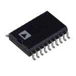
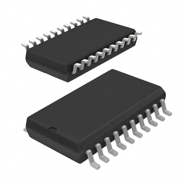
| 供应商器件封装 | 20-SOIC |
| 共模瞬态抗扰度(最小值) | 25kV/µs |
| 关闭 | No Shutdown |
| 包装 | 管件 |
| 协议 | RS422,RS485 |
| 双工 | 全 |
| 商标 | Analog Devices |
| 安装类型 | 表面贴装 |
| 安装风格 | SMD/SMT |
| 封装 | Tube |
| 封装/外壳 | 20-SOIC(0.295",7.50mm 宽) |
| 封装/箱体 | SOIC-20 |
| 工作温度 | -40°C ~ 85°C |
| 工厂包装数量 | 37 |
| 技术 | 磁耦合 |
| 接收器滞后 | 15mV |
| 数据速率 | 16Mbps |
| 最大工作温度 | + 85 C |
| 最大数据速率 | 16 Mb/s |
| 最小工作温度 | - 40 C |
| 标准包装 | 37 |
| 电压-电源 | 3.3V,5V |
| 电压-隔离 | 2500Vrms |
| 电源电压-最大 | 5.5 V |
| 电源电压-最小 | 3 V |
| 电源电流 | 230 mA |
| 类型 | RS422, RS485 |
| 系列 | ADM2582E |
| 绝缘电压 | 2.5 kVrms |
| 脉宽失真(最大) | - |
| 输入-输入侧1/输入侧2 | 2/1 |
| 通道数 | 3 |
| 通道数量 | 3 Channel |
| 通道类型 | 单向 |
| 隔离式电源 | 是 |
| 驱动器/接收器数 | 1/1 |


- 商务部:美国ITC正式对集成电路等产品启动337调查
- 曝三星4nm工艺存在良率问题 高通将骁龙8 Gen1或转产台积电
- 太阳诱电将投资9.5亿元在常州建新厂生产MLCC 预计2023年完工
- 英特尔发布欧洲新工厂建设计划 深化IDM 2.0 战略
- 台积电先进制程称霸业界 有大客户加持明年业绩稳了
- 达到5530亿美元!SIA预计今年全球半导体销售额将创下新高
- 英特尔拟将自动驾驶子公司Mobileye上市 估值或超500亿美元
- 三星加码芯片和SET,合并消费电子和移动部门,撤换高东真等 CEO
- 三星电子宣布重大人事变动 还合并消费电子和移动部门
- 海关总署:前11个月进口集成电路产品价值2.52万亿元 增长14.8%


PDF Datasheet 数据手册内容提取
Signal and Power Isolated RS-485 Transceiver with ±15 kV ESD Protection Data Sheet ADM2582E/ADM2587E FEATURES FUNCTIONAL BLOCK DIAGRAM Isolated RS-485/RS-422 transceiver, configurable as half or VCC VISOOUT full duplex isoPower DC-TO-DCCONVERTER isoPower integrated isolated dc-to-dc converter ±15 kV ESD protection on RS-485 input/output pins OSCILLATOR RECTIFIER Complies with ANSI/TIA/EIA-485-A-98 and ISO 8482:1987(E) ADM2582E data rate: 16 Mbps REGULATOR VISOIN ADM2587E data rate: 500 kbps 5 V or 3.3 V operation Connect up to 256 nodes on one bus DIGITAL ISOLATIONiCoupler TRANSCEIVER Open- and short-circuit, fail-safe receiver inputs Y TxD ENCODE DECODE D High common-mode transient immunity: >25 kV/µs Z Thermal shutdown protection Safety and regulatory approvals DE ENCODE DECODE UL recognition: 2500 V rms for 1 minute per UL 1577 VDE Certificates of Conformity A RxD DECODE ENCODE R DIN EN 60747-5-2 (VDE 0884 Part 2): 2003-01 B V = 560 V peak IORM Operating temperature range: −40°C to +85°C RE ADM2582E/ADM2587E H ighly integrated, 20-lead, wide-body SOIC package GND1 ISBOALRARTIEIORN GND2 08111-001 Figure 1. APPLICATIONS Isolated RS-485/RS-422 interfaces Industrial field networks Multipoint data transmission systems GENERAL DESCRIPTION The ADM2582E/ADM2587E are fully integrated signal and The ADM2582E/ADM2587E driver has an active high enable. power isolated data transceivers with ±15 kV ESD protection An active low receiver enable is also provided, which causes the and are suitable for high speed communication on multipoint receiver output to enter a high impedance state when disabled. transmission lines. The ADM2582E/ADM2587E include an The devices have current limiting and thermal shutdown integrated isolated dc-to-dc power supply, which eliminates the features to protect against output short circuits and situations need for an external dc-to-dc isolation block. where bus contention may cause excessive power dissipation. They are designed for balanced transmission lines and comply The parts are fully specified over the industrial temperature with ANSI/TIA/EIA-485-A-98 and ISO 8482:1987(E). range and are available in a highly integrated, 20-lead, wide-body SOIC package. The devices integrate Analog Devices, Inc., iCoupler® technology to combine a 3-channel isolator, a three-state differential line driver, The ADM2582E/ADM2587E contain isoPower technology that a differential input receiver, and Analog Devices isoPower® dc-to- uses high frequency switching elements to transfer power through dc converter into a single package. The devices are powered by a the transformer. Special care must be taken during printed circuit single 5 V or 3.3 V supply, realizing a fully integrated signal and board (PCB) layout to meet emissions standards. Refer to the power isolated RS-485 solution. AN-0971 Application Note, Control of Radiated Emissions with isoPower Devices, for details on board layout considerations. Rev. G Document Feedback Information furnished by Analog Devices is believed to be accurate and reliable. However, no responsibility is assumed by Analog Devices for its use, nor for any infringements of patents or other One Technology Way, P.O. Box 9106, Norwood, MA 02062-9106, U.S.A. rights of third parties that may result from its use. Specifications subject to change without notice. No license is granted by implication or otherwise under any patent or patent rights of Analog Devices. Tel: 781.329.4700 ©2009–2018 Analog Devices, Inc. All rights reserved. Trademarks and registered trademarks are the property of their respective owners. Technical Support www.analog.com
ADM2582E/ADM2587E Data Sheet TABLE OF CONTENTS Features .............................................................................................. 1 Test Circuits ..................................................................................... 13 Applications ....................................................................................... 1 Switching Characteristics .............................................................. 14 Functional Block Diagram .............................................................. 1 Circuit Description......................................................................... 15 General Description ......................................................................... 1 Signal Isolation ........................................................................... 15 Revision History ............................................................................... 2 Power Isolation ........................................................................... 15 Specifications ..................................................................................... 4 Truth Tables................................................................................. 15 ADM2582E Timing Specifications ............................................ 5 Thermal Shutdown .................................................................... 15 ADM2587E Timing Specifications ............................................ 5 Open- and Short-Circuit, Fail-Safe Receiver Inputs.............. 15 ADM2582E/ADM2587E Package Characteristics ................... 5 DC Correctness and Magnetic Field Immunity ........................... 15 ADM2582E/ADM2587E Regulatory Information .................. 6 Applications Information .............................................................. 17 ADM2582E/ADM2587E Insulation and Safety-Related PCB Layout and Electromagnetic Interference (EMI) .......... 17 Specifications ................................................................................ 6 Insulation Lifetime ..................................................................... 18 ADM2582E/ADM2587E VDE 0884 Insulation Isolated Power Supply Considerations .................................... 19 Characteristics .............................................................................. 6 Typical Applications ................................................................... 20 Absolute Maximum Ratings ............................................................ 7 Outline Dimensions ....................................................................... 22 ESD Caution .................................................................................. 7 Ordering Guide .......................................................................... 22 Pin Configuration and Function Descriptions ............................. 8 Typical Performance Characteristics ............................................. 9 REVISION HISTORY 5/2018—Rev. F to Rev. G 6/2011—Rev. B to Rev. C Changes to Table 10 .......................................................................... 8 Changes to Features Section and Figure 1 ..................................... 1 Deleted Electromagnetic Interference (EMI) Considerations Changes to Table 4 ............................................................................. 4 Section .............................................................................................. 16 Changes to Table 5 ............................................................................. 5 Changes to PCB Layout and Electromagnetic Interference Deleted Table 6; Renumbered Sequentially ................................... 5 (EMI) Section .................................................................................. 17 Added Thermal Resistance θ Parameter, Table 8 ....................... 6 JA Changes to Figure 35 ...................................................................... 18 Changes to Table 9 ............................................................................. 6 Changes to PCB Layout Reference ............................................... 19 Changes to Table 10 .......................................................................... 7 Changes to Ordering Guide .......................................................... 22 Changes to Table 13 ....................................................................... 14 Moved DC Correctness and Magnetic Field Immunity 9/2016—Rev. E to Rev. F Section .............................................................................................. 14 Changes to Ordering Guide .......................................................... 20 Changes to PCB Layout Section and Figure 35 .......................... 16 Changes to Figure 39 ...................................................................... 17 10/2014—Rev. D to Rev. E Changes to Typical Applications Section and Figure 40 ........... 18 Changes to Table 12 ........................................................................ 14 9/2014—Rev. C to Rev. D Changes to Figure 9 .......................................................................... 9 Rev. G | Page 2 of 22
Data Sheet ADM2582E/ADM2587E 3/2011—Rev. A to Rev. B Changes to Differential Output Voltage, Loaded Parameter, Removed Pending from Safety and Regulatory Table 1 ................................................................................................. 3 Approvals ........................................................................ Throughout Changes to Table 5 ............................................................................ 5 Changed Minimum External Air Gap (Clearance) Value and Added Table 6; Renumbered Sequentially ..................................... 5 Minimum External Tracking (Creepage) Value ............................ 5 Change to Pin 8 Description, Table 11 ........................................... 7 Added Text to the ADM2582E/ADM2587E VDE 0884 Changes to Figure 5 and Figure 6 ................................................... 8 Insulation Characteristics Section ................................................. 5 Changes to Table 13 and Table 14 ................................................. 14 9/2010—Rev. 0 to Rev. A 9/2009—Revision 0: Initial Version Changes to Features Section ............................................................ 1 Rev. G | Page 3 of 22
ADM2582E/ADM2587E Data Sheet SPECIFICATIONS All voltages are relative to their respective ground; 3.0 ≤ V ≤ 5.5 V. All minimum/maximum specifications apply over the entire CC recommended operation range, unless otherwise noted. All typical specifications are at T = 25°C, V = 5 V unless otherwise noted. A CC Table 1. Parameter Symbol Min Typ Max Unit Test Conditions ADM2587E SUPPLY CURRENT I CC Data Rate ≤ 500 kbps 90 mA V = 3.3 V, 100 Ω load between Y and CC Z 72 mA V = 5 V, 100 Ω load between Y and Z CC 125 mA V = 3.3 V, 54 Ω load between Y and CC Z 98 mA V = 5 V, 54 Ω load between Y and Z CC 120 mA 120 Ω load between Y and Z ADM2582E SUPPLY CURRENT I CC Data Rate = 16 Mbps 150 mA 120 Ω load between Y and Z 230 mA 54 Ω load between Y and Z ISOLATED SUPPLY VOLTAGE V 3.3 ISOUT DRIVER Differential Outputs Differential Output Voltage, Loaded |V | 2.0 3.6 V R = 100 Ω (RS-422), see Figure 23 OD2 L 1.5 3.6 V R = 54 Ω (RS-485), see Figure 23 L |V | 1.5 3.6 V −7 V ≤ V ≤ 12 V, see Figure 24 OD3 TEST1 Δ|V | for Complementary Output States Δ|V | 0.2 V R = 54 Ω or 100 Ω, see Figure 23 OD OD L Common-Mode Output Voltage V 3.0 V R = 54 Ω or 100 Ω, see Figure 23 OC L Δ|V | for Complementary Output States Δ|V | 0.2 V R = 54 Ω or 100 Ω, see Figure 23 OC OC L Short-Circuit Output Current I 200 mA OS Output Leakage Current (Y, Z) IO 30 µA DE = 0 V, RE = 0 V, VCC = 0 V or 3.6 V, V = 12 V IN −30 µA DE = 0 V, RE = 0 V, VCC = 0 V or 3.6 V, V = −7 V IN Logic Inputs DE, RE, TxD Input Threshold Low VIL 0.3 × VCC V DE, RE, TxD Input Threshold High VIH 0.7 × VCC V DE, RE, TxD Input Current II −10 0.01 10 µA DE, RE, TxD RECEIVER Differential Inputs Differential Input Threshold Voltage V −200 −125 −30 mV −7 V < V < +12 V TH CM Input Voltage Hysteresis V 15 mV V = 0 V HYS OC Input Current (A, B) I 125 µA DE = 0 V, V = 0 V or 3.6 V, V = 12 V I CC IN −100 µA DE = 0 V, V = 0 V or 3.6 V, V = −7 V CC IN Line Input Resistance R 96 kΩ −7 V < V < +12 V IN CM Logic Outputs Output Voltage Low V 0.2 0.4 V I = 1.5 mA, V − V = −0.2 V OL O A B Output Voltage High V V − 0.3 V − 0.2 V I = −1.5 mA, V − V = 0.2 V OH CC CC O A B Short-Circuit Current 100 mA COMMON-MODE TRANSIENT IMMUNITY1 25 kV/µs V = 1 kV, transient magnitude = 800 V CM 1 CM is the maximum common-mode voltage slew rate that can be sustained while maintaining specification-compliant operation. VCM is the common-mode potential difference between the logic and bus sides. The transient magnitude is the range over which the common-mode is slewed. The common-mode voltage slew rates apply to both rising and falling common-mode voltage edges. Rev. G | Page 4 of 22
Data Sheet ADM2582E/ADM2587E ADM2582E TIMING SPECIFICATIONS T = −40°C to +85°C. A Table 2. Parameter Symbol Min Typ Max Unit Test Conditions DRIVER Maximum Data Rate 16 Mbps Propagation Delay, Low to High t 63 100 ns R = 54 Ω, C = C = 100 pF, see Figure 25 and Figure 29 DPLH L L1 L2 Propagation Delay, High to Low t 64 100 ns R = 54 Ω, C = C = 100 pF, see Figure 25 and Figure 29 DPHL L L1 L2 Output Skew t 1 8 ns R = 54 Ω, C = C = 100 pF, see Figure 25 and Figure 29 SKEW L L1 L2 Rise Time/Fall Time t , t 15 ns R = 54 Ω, C = C = 100 pF, see Figure 25 and Figure 29 DR DF L L1 L2 Enable Time t , t 120 ns R = 110 Ω, C = 50 pF, see Figure 26 and Figure 31 ZL ZH L L Disable Time t , t 150 ns R = 110 Ω, C = 50 pF, see Figure 26 and Figure 31 LZ HZ L L RECEIVER Propagation Delay, Low to High t 94 110 ns C = 15 pF, see Figure 27 and Figure 30 RPLH L Propagation Delay, High to Low t 95 110 ns C = 15 pF, see Figure 27 and Figure 30 RPHL L Output Skew1 t 1 12 ns C = 15 pF, see Figure 27 and Figure 30 SKEW L Enable Time t , t 15 ns R = 1 kΩ, C = 15 pF, see Figure 28 and Figure 32 ZL ZH L L Disable Time t , t 15 ns R = 1 kΩ, C = 15 pF, see Figure 28 and Figure 32 LZ HZ L L 1 Guaranteed by design. ADM2587E TIMING SPECIFICATIONS T = −40°C to +85°C. A Table 3. Parameter Symbol Min Typ Max Unit Test Conditions DRIVER Maximum Data Rate 500 kbps Propagation Delay, Low to High t 250 503 700 ns R = 54 Ω, C = C = 100 pF, see Figure 25 and Figure 29 DPLH L L1 L2 Propagation Delay, High to Low t 250 510 700 ns R = 54 Ω, C = C = 100 pF, see Figure 25 and Figure 29 DPHL L L1 L2 Output Skew t 7 100 ns R = 54 Ω, C = C = 100 pF, see Figure 25 and Figure 29 SKEW L L1 L2 Rise Time/Fall Time t , t 200 1100 ns R = 54 Ω, C = C = 100 pF, see Figure 25 and Figure 29 DR DF L L1 L2 Enable Time t , t 2.5 µs R = 110 Ω, C = 50 pF, see Figure 26 and Figure 31 ZL ZH L L Disable Time t , t 200 ns R = 110 Ω, C = 50 pF, see Figure 26 and Figure 31 LZ HZ L L RECEIVER Propagation Delay, Low to High t 91 200 ns C = 15 pF, see Figure 27 and Figure 30 RPLH L Propagation Delay, High to Low t 95 200 ns C = 15 pF, see Figure 27 and Figure 30 RPHL L Output Skew t 4 30 ns C = 15 pF, see Figure 27 and Figure 30 SKEW L Enable Time t , t 15 ns R = 1 kΩ, C = 15 pF, see Figure 28 and Figure 32 ZL ZH L L Disable Time t , t 15 ns R = 1 kΩ, C = 15 pF, see Figure 28 and Figure 32 LZ HZ L L ADM2582E/ADM2587E PACKAGE CHARACTERISTICS Table 4. Parameter Symbol Min Typ Max Unit Test Conditions Resistance (Input-to-Output)1 R 1012 Ω I-O Capacitance (Input-to-Output)1 C 3 pF f = 1 MHz I-O Input Capacitance2 C 4 pF I 1 Device considered a 2-terminal device: short together Pin 1 to Pin 10 and short together Pin 11 to Pin 20. 2 Input capacitance is from any input data pin to ground. Rev. G | Page 5 of 22
ADM2582E/ADM2587E Data Sheet ADM2582E/ADM2587E REGULATORY INFORMATION Table 5. ADM2582E/ADM2587E Approvals Organization Approval Type Notes UL Recognized under the Component In accordance with UL 1577, each ADM2582E/ADM2587E is proof tested Recognition Program of Underwriters by applying an insulation test voltage ≥ 3000 V rms for 1 second. Laboratories, Inc. VDE Certified according to DIN EN 60747-5-2 In accordance with DIN EN 60747-5-2, each ADM2582E/ADM2587E is (VDE 0884 Part 2): 2003-01 proof tested by applying an insulation test voltage ≥ 1050 VPEAK for 1 second. ADM2582E/ADM2587E INSULATION AND SAFETY-RELATED SPECIFICATIONS Table 6. Parameter Symbol Value Unit Conditions Rated Dielectric Insulation Voltage 2500 V rms 1-minute duration Minimum External Air Gap (Clearance) L(I01) 7.7 mm Measured from input terminals to output terminals, shortest distance through air Minimum External Tracking (Creepage) L(I02) 7.6 mm Measured from input terminals to output terminals, shortest distance along body Minimum Internal Gap (Internal Clearance) 0.017 min mm Insulation distance through insulation Tracking Resistance (Comparative Tracking Index) CTI >175 V DIN IEC 112/VDE 0303-1 Isolation Group IIIa Material Group (DIN VDE 0110: 1989-01, Table 1) ADM2582E/ADM2587E VDE 0884 INSULATION CHARACTERISTICS This isolator is suitable for basic electrical isolation only within the safety limit data. Maintenance of the safety data must be ensured by means of protective circuits. An asterisk (*) on packages denotes VDE 0884 Part 2 approval. Table 7. Description Conditions Symbol Characteristic Unit CLASSIFICATIONS Installation Classification per DIN VDE 0110 for Rated Mains Voltage ≤150 V rms I to IV ≤300 V rms I to III ≤400 V rms I to II Climatic Classification 40/85/21 Pollution Degree DIN VDE 0110, see Table 1 2 VOLTAGE Maximum Working Insulation Voltage V 560 V peak IORM Input-to-Output Test Voltage V PR Method b1 V × 1.875 = V , 100% production tested, 1050 V peak IORM PR t = 1 sec, partial discharge < 5 pC m Method a After Environmental Tests, Subgroup 1 V × 1.6 = V , t = 60 sec, partial discharge < 5 pC 896 V peak IORM PR m After Input and/or Safety Test, V × 1.2 = V , t = 60 sec, partial discharge < 5 pC 672 V peak IORM PR m Subgroup 2/Subgroup 3 Highest Allowable Overvoltage Transient overvoltage, t = 10 sec V 4000 V peak TR TR SAFETY-LIMITING VALUES Maximum value allowed in the event of a failure Case Temperature T 150 °C S Input Current I, 265 mA S INPUT Output Current I, 335 mA S OUTPUT Insulation Resistance at T V = 500 V R >109 Ω S IO S Rev. G | Page 6 of 22
Data Sheet ADM2582E/ADM2587E ABSOLUTE MAXIMUM RATINGS T = 25°C, unless otherwise noted. All voltages are relative to A Table 9. Maximum Continuous Working Voltage1 their respective ground. Parameter Max Unit Reference Standard AC Voltage Table 8. Bipolar Waveform 424 V peak 50-year minimum Parameter Rating lifetime V −0.5 V to +7 V CC Unipolar Waveform Digital Input Voltage (DE, RE, TxD) −0.5 V to V + 0.5 V DD Basic Insulation 560 V peak Maximum approved Digital Output Voltage (RxD) −0.5 V to V + 0.5 V DD working voltage per Driver Output/Receiver Input Voltage −9 V to +14 V VDE 0884 Part 2 Operating Temperature Range −40°C to +85°C DC Voltage Storage Temperature Range −55°C to +150°C Basic Insulation 560 V peak Maximum approved ESD (Human Body Model) on ±15 kV working voltage per A, B, Y, and Z pins VDE 0884 Part 2 ESD (Human Body Model) on Other Pins ±2 kV 1 Refers to continuous voltage magnitude imposed across the isolation Thermal Resistance θ 50°C/W JA barrier. See the Insulation Lifetime section for more details. Lead Temperature Soldering (10 sec) 260°C ESD CAUTION Vapor Phase (60 sec) 215°C Infrared (15 sec) 220°C Stresses at or above those listed under Absolute Maximum Ratings may cause permanent damage to the product. This is a stress rating only; functional operation of the product at these or any other conditions above those indicated in the operational section of this specification is not implied. Operation beyond the maximum operating conditions for extended periods may affect product reliability. Rev. G | Page 7 of 22
ADM2582E/ADM2587E Data Sheet PIN CONFIGURATION AND FUNCTION DESCRIPTIONS GND1 1 20 GND2 VCC 2 19 VISOIN GND1 3 18 A ADM2582E RxD 4 17 B ADM2587E RE 5 TOP VIEW 16 GND2 DE 6 (Not to Scale) 15 Z TxD 7 14 GND2 VCC 8 13 Y GND1 9 12 VISOOUT GND1 10 11 GND2 N1 . O PCTIONENS 1N2E ACNTDE DP IENX 1T9E MRUNSATL LBYE. 08111-002 Figure 2. Pin Configuration Table 10. Pin Function Description Pin No. Mnemonic Description 1 GND Ground, Logic Side. 1 2 V Logic Side Power Supply. It is recommended that a 0.1 µF and a 0.01 µF decoupling capacitor be fitted between CC Pin 2 and Pin 1. See Figure 35 for layout recommendations. 3 GND Ground, Logic Side. 1 4 RxD Receiver Output Data. This output is high when (A − B) ≥ −30 mV and low when (A − B) ≤ –200 mV. The output is tristated when the receiver is disabled, that is, when RE is driven high. 5 RE Receiver Enable Input. This is an active-low input. Driving this input low enables the receiver; driving it high disables the receiver. 6 DE Driver Enable Input. Driving this input high enables the driver; driving it low disables the driver. 7 TxD Driver Input. Data to be transmitted by the driver is applied to this input. 8 V Logic Side Power Supply. It is recommended that a 0.1 µF and a 10 µF decoupling capacitor be fitted between CC Pin 8 and Pin 9. See Figure 35 for layout recommendations. 9 GND Ground, Logic Side. 1 10 GND Ground, Logic Side. 1 11, 14 GND Ground for Isolated DC-to-DC Converter. It is recommended to connect Pin 11 and Pin 14 together through one 2 ferrite bead to PCB ground. See Figure 35 for layout recommendations. 12 V Isolated Power Supply Output. This pin must be connected externally to V . It is recommended that a reservoir ISOOUT ISOIN capacitor of 10 µF and a decoupling capacitor of 0.1 µF be fitted between Pin 12 and Pin 11. 13 Y Driver Noninverting Output 15 Z Driver Inverting Output 16 GND Ground, Bus Side. Do not connect this pin to Pin 14 and Pin 11. See Figure 35 for layout recommendations. 2 17 B Receiver Inverting Input. 18 A Receiver Noninverting Input. 19 V Isolated Power Supply Input. This pin must be connected externally to V . It is recommended that a ISOIN ISOOUT 0.1 µF and a 0.01 µF decoupling capacitor be fitted between Pin 19 and Pin 20. Connect this pin through a ferrite bead and short trace length to V for operation. See Figure 35 for layout recommendations. ISOOUT 20 GND Ground, Bus Side. 2 Rev. G | Page 8 of 22
Data Sheet ADM2582E/ADM2587E TYPICAL PERFORMANCE CHARACTERISTICS 180 140 160 120 A)140 RL = 54Ω A) RL = 54Ω m m 100 NT, I(CC110200 RL = 120Ω NT, I(CC 80 RL = 120Ω E E R R CUR 80 CUR 60 PLY 60 NO LOAD PLY UP UP 40 S 40 S NO LOAD 20 20 0–40 –15 TEM10PERATURE3 (5°C) 60 85 08111-103 0–40 –15 TEM10PERATURE3 (5°C) 60 85 08111-105 Figure 3. ADM2582E Supply Current (ICC) vs. Temperature Figure 6. ADM2587E Supply Current (ICC) vs. Temperature (Data Rate = 16 Mbps, DE = 3.3 V, VCC = 3.3 V) (Data Rate = 500 kbps, DE = 3.3 V, VCC = 3.3 V) 140 72 70 120 RL = 54Ω ns)68 A) Y ( CURRENT, I(mCC1068000 RL = 120Ω PAGATION DELA66660246 tDPHtLDPLH PLY NO LOAD PRO58 UP 40 ER 56 S V RI54 20 D 52 0–40 –15 TEM10PERATURE3 (5°C) 60 85 08111-104 50–40 –15 TEM10PERATURE3 5(°C) 60 85 08111-107 Figure 4. ADM2582E Supply Current (ICC) vs. Temperature Figure 7. ADM2582E Differential Driver Propagation Delay vs. Temperature (Data Rate = 16 Mbps, DE = 5 V, VCC = 5 V) 120 600 580 100 s) A) RL = 54Ω Y (n560 m A RENT, I(CC 6800 RL = 120Ω ATION DEL555024000 tDPHL tDPLH R G U A PLY C 40 PROP480 SUP NO LOAD VER 460 20 DRI440 420 0–40 –15 TEM10PERATURE3 (5°C) 60 85 08111-106 400–40 –15 TEM10PERATURE3 5(°C) 60 85 08111-108 Figure 5. ADM2587E Supply Current (ICC) vs. Temperature Figure 8. ADM2587E Differential Driver Propagation Delay vs. Temperature (Data Rate = 500 kbps, DE = 5 V, VCC = 5 V) Rev. G | Page 9 of 22
ADM2582E/ADM2587E Data Sheet 60 TxD 50 A) m T (40 N E R 1 UR30 C T U Y TP20 U O Z 10 3 CCHH13 22..00VV CH2 2.0V M10.00ns A CH1 1.28V 08111-109 00 1 OUTP2UT VOLTAG3E (V) 4 5 08111-112 Figure 9. ADM2582E Driver Propagation Delay Figure 12. Receiver Output Current vs. Receiver Output Low Voltage 4.75 4.74 4.73 V) 4.72 E( G A 4.71 TxD LT 1 VO 4.70 T PU 4.69 Z UT O 4.68 Y 4.67 3 4.66 CCHH13 22..00VV CH2 2.0V M200ns A CH1 2.56V 08111-110 4.65–40 –15 TEM10PERATURE3 5(°C) 60 85 08111-113 Figure 10. ADM2587E Driver Propagation Delay Figure 13. Receiver Output High Voltage vs. Temperature 0 0.32 –10 0.30 OUTPUT CURRENT (mA) ––––54320000 OUTPUT VOLTAGE (V) 000...222468 –60 0.22 –700 1 OUTP2UT VOLTAG3E (V) 4 5 08111-111 0.20–40 –15 TEM10PERATURE3 5(°C) 60 85 08111-114 Figure 11. Receiver Output Current vs. Receiver Output High Voltage Figure 14. Receiver Output Low Voltage vs. Temperature Rev. G | Page 10 of 22
Data Sheet ADM2582E/ADM2587E 100 99 s) B Y (n 98 A L E 97 D N O 96 1 A AGATI 95 tRPHL P RxD RO 94 P ER 93 V CEI 92 3 RE 91 tRPLH CCHH13 22..00VV CH2 2.0V M10.00ns A CH1 2.56V 08111-115 90–40 –15 TEM10PERATURE3 5(°C) 60 85 08111-118 Figure 15. ADM2582E Receiver Propagation Delay Figure 18. ADM2587E Receiver Propagation Delay vs. Temperature 3.33 A 3.32 V) E ( AG3.31 T L O B Y V3.30 1 PL P U3.29 S D E NO LOAD T LA3.28 RL = 120Ω RxD ISO RL = 54Ω 3 3.27 CCHH13 22..00VV CH2 2.0V M10.00ns A CH1 2.56V 08111-116 3.26–40 –15 TEM10PERATURE3 (5°C) 60 85 08111-119 Figure 16. ADM2587E Receiver Propagation Delay Figure 19. ADM2582E Isolated Supply Voltage vs. Temperature (VCC = 3.3 V, Data Rate = 16 Mbps) 98 3.36 3.35 s) AY (n 97 E (V)3.34 L G ATION DE 96 tRPHL Y VOLTA33..3332 PROPAG 95 tRPLH D SUPPL33..3310 CEIVER 94 SOLATE33..2289 NO LOAD RE 93 I RL = 120Ω 3.27 RL = 54Ω 92–40 –15 TEM10PERATURE3 (5°C) 60 85 08111-117 3.26–40 –15 TEM10PERATURE3 (5°C) 60 85 08111-120 Figure 17. ADM2582E Receiver Propagation Delay vs. Temperature Figure 20. ADM2582E Isolated Supply Voltage vs. Temperature (VCC = 5 V, Data Rate = 16 Mbps) Rev. G | Page 11 of 22
ADM2582E/ADM2587E Data Sheet 60 40 RL = 54Ω RL = 54Ω 35 A) 50 A) m m T( T( 30 N N URRE 40 RL = 120Ω URRE 25 RL = 120Ω C C LY 30 LY 20 P P P P U U ED S 20 NO LOAD ED S 15 LAT LAT 10 O O NO LOAD IS 10 IS 5 0–40 –15 TEM10PERATURE3 (5°C) 60 85 08111-121 0–40 –15 TEM10PERATURE3 (5°C) 60 85 08111-122 Figure 21. ADM2582E Isolated Supply Current vs. Temperature Figure 22. ADM2587E Isolated Supply Current vs. Temperature (VCC = 3.3 V, Data Rate = 16 Mbps) (VCC = 3.3 V, Data Rate = 500 kbps) Rev. G | Page 12 of 22
Data Sheet ADM2582E/ADM2587E TEST CIRCUITS Y RL 2 TxD VOD2 VOUT VCC Z R2L Y RL VOC TxD S1 110Ω S2 08111-003 DE Z C50LpF 08111-006 Figure 26. Driver Enable/Disable Figure 23. Driver Voltage Measurement Y 375Ω A TxD VOD3 60Ω Z 375Ω VTEST 08111-004 FigurBe 27. RReEceiver PropagCaLtionV ODUeTla08111-007y Figure 24. Driver Voltage Measurement +1.5V VCC Y CL S1 TxD RL –1.5V RL S2 Z CL RE CL VOUT 08111-005 RE INFigure 28. Receiver Enable/Disable 08111-008 Figure 25. Driver Propagation Delay Rev. G | Page 13 of 22
ADM2582E/ADM2587E Data Sheet SWITCHING CHARACTERISTICS VCC VCC/2 VCC/2 0V tDPLH tDPHL VCC Z 1/2VO DE 0.5VCC 0.5VCC VO 0V Y tZL 2.3V tLZ +VO 90% POINT 90% POINT Y, Z VOL+ 0.5V VDIFF= V(Y)– V(Z) VOL VDIFF tZH 2.3V tHZ t–SVKOEW = │tD1P0H%L P–OtDINPLTH│tDR tDF 10% POINT 08111-009 Y, Z VOH– 0.5V VOH 08111-011 Figure 29. Driver Propagation Delay, Rise/Fall Timing Figure 31. Driver Enable/Disable Timing 0.7VCC RE 0.5VCC 0.5VCC 0.3VCC A – B 0V 0V tZL tLZ 1.5V tRPLH tRPHL RO OUTPUT LOW VOL+ 0.5V VOL VOH tZH tHZ OUTPUT HIGH RxD 1.5V tSKEW = |tRPLH–tRPHL| 1.5V VOL 08111-010 R0OV 1.5V VOH– 0.5V VOH 08111-012 Figure 30. Receiver Propagation Delay Figure 32. Receiver Enable/Disable Timing Rev. G | Page 14 of 22
Data Sheet ADM2582E/ADM2587E CIRCUIT DESCRIPTION SIGNAL ISOLATION Table 13. Receiving (see Table 11 for Abbreviations) The ADM2582E/ADM2587E signal isolation is implemented on Inputs Output the logic side of the interface. The part achieves signal isolation A − B RE RxD by having a digital isolation section and a transceiver section ≥ −0.03 V L or NC H (see Figure 1). Data applied to the TxD and DE pins and referenced ≤ −0.2 V L or NC L to logic ground (GND1) are coupled across an isolation barrier −0.2 V < A − B < −0.03 V L or NC X to appear at the transceiver section referenced to isolated ground Inputs open L or NC H (GND2). Similarly, the single-ended receiver output signal, X H Z referenced to isolated ground in the transceiver section, is coupled across the isolation barrier to appear at the RXD pin THERMAL SHUTDOWN referenced to logic ground. The ADM2582E/ADM2587E contain thermal shutdown circuitry POWER ISOLATION that protects the parts from excessive power dissipation during fault conditions. Shorting the driver outputs to a low impedance The ADM2582E/ADM2587E power isolation is implemented source can result in high driver currents. The thermal sensing using an isoPower integrated isolated dc-to-dc converter. The circuitry detects the increase in die temperature under this dc-to-dc converter section of the ADM2582E/ADM2587E works condition and disables the driver outputs. This circuitry is on principles that are common to most modern power supplies. It designed to disable the driver outputs when a die temperature is a secondary side controller architecture with isolated pulse-width of 150°C is reached. As the device cools, the drivers are reenabled modulation (PWM) feedback. V power is supplied to an CC at a temperature of 140°C. oscillating circuit that switches current into a chip-scale air core transformer. Power transferred to the secondary side is rectified OPEN- AND SHORT-CIRCUIT, FAIL-SAFE RECEIVER and regulated to 3.3 V. The secondary (V ) side controller INPUTS ISO regulates the output by creating a PWM control signal that is The receiver inputs have open- and short-circuit, fail-safe sent to the primary (V ) side by a dedicated iCoupler data CC features that ensure that the receiver output is high when the channel. The PWM modulates the oscillator circuit to control inputs are open or shorted. During line-idle conditions, when no the power being sent to the secondary side. Feedback allows for driver on the bus is enabled, the voltage across a terminating significantly higher power and efficiency. resistance at the receiver input decays to 0 V. With traditional TRUTH TABLES transceivers, receiver input thresholds specified between −200 mV and +200 mV mean that external bias resistors are required on the The truth tables in this section use the abbreviations found in A and B pins to ensure that the receiver outputs are in a known Table 11. state. The short-circuit, fail-safe receiver input feature eliminates Table 11. Truth Table Abbreviations the need for bias resistors by specifying the receiver input threshold Letter Description between −30 mV and −200 mV. The guaranteed negative threshold H High level means that when the voltage between A and B decays to 0 V, the L Low level receiver output is guaranteed to be high. X Don’t care DC CORRECTNESS AND MAGNETIC FIELD IMMUNITY Z High impedance (off) The digital signals transmit across the isolation barrier using NC Disconnected iCoupler technology. This technique uses chip-scale transformer windings to couple the digital signals magnetically from one Table 12. Transmitting (see Table 11 for Abbreviations) side of the barrier to the other. Digital inputs are encoded into Inputs Outputs waveforms that are capable of exciting the primary transformer DE TxD Y Z winding. At the secondary winding, the induced waveforms are H H H L decoded into the binary value that was originally transmitted. H L L H Positive and negative logic transitions at the isolator input cause L X Z Z narrow (~1 ns) pulses to be sent to the decoder via the transformer. The decoder is bistable and is, therefore, either set or reset by the pulses, indicating input logic transitions. In the absence of logic transitions at the input for more than 1 µs, periodic sets of refresh pulses indicative of the correct input state are sent to ensure dc correctness at the output. If the decoder receives no internal pulses of more than approximately 5 µs, the input side is assumed to be Rev. G | Page 15 of 22
ADM2582E/ADM2587E Data Sheet unpowered or nonfunctional, in which case, the isolator output For example, at a magnetic field frequency of 1 MHz, the is forced to a default state by the watchdog timer circuit. maximum allowable magnetic field of 0.2 kgauss induces a voltage of 0.25 V at the receiving coil. This is about 50% of the This situation should occur in the ADM2582E/ADM2587E sensing threshold and does not cause a faulty output transition. devices only during power-up and power-down operations. The Similarly, if such an event occurs during a transmitted pulse limitation on the ADM2582E/ADM2587E magnetic field (and is of the worst-case polarity), it reduces the received pulse immunity is set by the condition in which induced voltage in from >1.0 V to 0.75 V, which is still well above the 0.5 V sensing the transformer receiving coil is sufficiently large to either threshold of the decoder. falsely set or reset the decoder. The following analysis defines the conditions under which this can occur. The preceding magnetic flux density values correspond to specific current magnitudes at given distances from the The 3.3 V operating condition of the ADM2582E/ADM2587E ADM2582E/ADM2587E transformers. Figure 34 expresses is examined because it represents the most susceptible mode of these allowable current magnitudes as a function of frequency operation. The pulses at the transformer output have an amplitude for selected distances. As shown in Figure 34, the ADM2582E/ of >1.0 V. The decoder has a sensing threshold of about 0.5 V, ADM2587E are extremely immune and can be affected only by thus establishing a 0.5 V margin in which induced voltages can extremely large currents operated at high frequency very close be tolerated. The voltage induced across the receiving coil is to the component. For the 1 MHz example, a 0.5 kA current must given by be placed 5 mm away from the ADM2582E/ADM2587E to affect V = (−dβ/dt)Σπr2; n = 1, 2, … , N n component operation. where: 1k β is magnetic flux density (gauss). A) DISTANCE = 1m N is the number of turns in the receiving coil. T (k 100 rn is the radius of the nth turn in the receiving coil (cm). EN R R Given the geometry of the receiving coil in the ADM2582E/ E CU 10 ADM2587E and an imposed requirement that the induced L AB DISTANCE = 100mm voltage be, at most, 50% of the 0.5 V margin at the decoder, a W O maximum allowable magnetic field is calculated as shown in L 1 L Figure 33. M A DISTANCE = 5mm U M 100 XI 0.1 A X M U L F E MAGNETIC Gauss) 101 0.011kFigure 341.0 MkMaAxGimNEuTm1IC0 A0 FkllIoELwDa FbRleE 1CQMuUrErNenCtY f (oHr1z V0)Marious 100M 08111-020 Lk Current-to-ADM2582E/ADM2587E Spacings ABY ( ALLOWDENSIT0.1 Nfreoqteu ethnacty ,i na ncyo mloboipnsa ftoiornmse odf bsytr opnrign tmeda gcnirectuici tf ibeolda radn (dP hCiBgh) UM traces can induce error voltages sufficiently large to trigger the XIM 0.01 thresholds of succeeding circuitry. Take care in the layout of A M such traces to avoid this possibility. 0.0011k 10kMAGNETI1C0 0FkIELD FREQ1MUENCY (Hz1)0M 100M 08111-019 Figure 33. Maximum Allowable External Magnetic Flux Density Rev. G | Page 16 of 22
Data Sheet ADM2582E/ADM2587E APPLICATIONS INFORMATION PCB LAYOUT AND ELECTROMAGNETIC frequency and the 360 MHz secondary side rectifying INTERFERENCE (EMI) frequency and harmonics. The ADM2582E/ADM2587E isolated RS-422/RS-485 transceiver To pass the EN55022 radiated emissions standard, the following contains an isoPower integrated dc-to-dc converter, requiring additional layout guidelines are recommended: no external interface circuitry for the logic interfaces. Power • Do not connect the V pin to a power plane; ISOOUT supply bypassing is required at the input and output supply pins connect between V and V using a PCB trace. ISOOUT ISOIN (see Figure 35). The power supply section of the ADM2582E/ Ensure that V (Pin 19) connects through the L1 ISOIN ADM2587E uses a 180 MHz oscillator frequency to pass power ferrite to V (Pin 12), as shown in Figure 35. ISOOUT efficiently through its chip-scale transformers. In addition, the • If using a four layer PCB, place an embedded stitching normal operation of the data section of the iCoupler introduces capacitor between GND and GND using internal switching transients on the power supply pins. 1 2 layers of the PCB planes. An embedded PCB capacitor Bypass capacitors are required for several operating frequencies. is created when two metal planes in a PCB overlap Noise suppression requires a low inductance, high frequency each other and are separated by dielectric material. capacitor, whereas ripple suppression and proper regulation This capacitor provides a return path for high require a large value capacitor. These capacitors are connected frequency common-mode noise currents across the between Pin 1 (GND) and Pin 2 (V ) and Pin 8 (V ) and 1 CC CC isolation gap. Pin 9 (GND) for V . The V and V capacitors are 1 CC ISOIN ISOOUT connected between Pin 11 (GND) and Pin 12 (V ) and • If using a two layer PCB, place a high voltage discrete 2 ISOOUT Pin 19 (VISOIN) and Pin 20 (GND2). To suppress noise and reduce capacitor that connects between GND1 (Pin 10) and ripple, a parallel combination of at least two capacitors is required GND2 (Pin 11). This capacitor provides a return path with the smaller of the two capacitors located closest to the device. for high frequency common-mode noise currents The recommended capacitor values are 0.1 µF and 10 µF for across the isolation gap. VISOOUT at Pin 11 and Pin 12 and VCC at Pin 8 and Pin 9. Capacitor • Ensure that GND2 (Pin 14) connects to GND2 (Pin 11) values of 0.01 µF and 0.1 µF are recommended for VISOIN at on the inside (device side) of the C1 100 nF capacitor. Pin 19 and Pin 20 and V at Pin 1 and Pin 2. The recommended CC • Ensure that the C1 capacitor connects between V best practice is to use a very low inductance ceramic capacitor, ISOOUT (Pin 12) and GND (Pin 11) on the device side of the or its equivalent, for the smaller value. The total lead length 2 L1 and L2 ferrites. between both ends of the capacitor and the input power supply pin should not exceed 10 mm. • Ensure that GND2 (Pin 16) is connected to GND2 (Pin 11) on the outside (bus side) of the L2 ferrite, as The dc-to-dc converter section of the ADM2582E/ADM2587E shown in Figure 35. components must operate, out of necessity, at a very high frequency to allow efficient power transfer through the small • Ensure that there is a keep out area for the GND 2 transformers. This creates high frequency currents that can plane in the PCB layout around the L1 and L2 ferrites. propagate in circuit board ground and power planes, causing edge The keep out area means there must not be a GND 2 and dipole radiation. fill on any layer below the L1 and L2 ferrites. The ADM2582E/ADM2587E features an internal split paddle, • Locate the power delivery circuit in close proximity to lead frame on the bus side. For the best noise suppression, filter the ADM2582E/ADM2587E device, so that the V CC both the GND2 pins (Pin 11 and Pin 14) and VISOOUT signals of trace is as short as possible. the integrated dc-to-dc converter for high frequency currents. See the AN-1349 Application Note, PCB Implementation Guidelines Use surface-mount ferrite beads in series with the signals before to Minimize Radiated Emissions on the ADM2582E/ADM2587E RS- routing back to the device. See Figure 35 for the recommended 485/RS-422 Transceivers, for more information. Evaluation boards PCB layout. The impedance of the ferrite bead is chosen to be and user guides are available for two layer and four layer PCB about 2 kΩ between the 100 MHz and 1 GHz frequency range EN55022 radiated emissions compliant designs. See UG-916 and to reduce the emissions at the 180 MHz primary switching UG-044 for more information. Rev. G | Page 17 of 22
ADM2582E/ADM2587E Data Sheet 10nF 10nF 100nF 100nF GND1 1 DIGITAL 20 GND2 VCC 2 ISOLATIONTRANSCEIVER 19 VISOIN GND1 3 18 PCB TRACE 4 R 17 CONNECTING PIN11AND PIN 14 D 5 16 GND2 6 15 7 14 VCC 8 13 L1 GND1 9 DC-TO-iDsoCP OCWONEVRERTER 12 VISOOUT GND1 10µF 10 11 GND2 100nF C1 L2 10µF 100nF FERRITE BEADS STITCHING CAPACITORACROSS ISOLATION BARRIER REQUIRED FOR EN55022/CISPR22 CLASS B PCB KEEP OUTAREA 08111-035 Figure 35. Recommended PCB Layout In applications involving high common-mode transients, ensure The insulation lifetime of the ADM2582E/ADM2587E depends that board coupling across the isolation barrier is minimized. on the voltage waveform type imposed across the isolation barrier. Furthermore, design the board layout such that any coupling The iCoupler insulation structure degrades at different rates, that does occur equally affects all pins on a given component depending on whether the waveform is bipolar ac, unipolar ac, side. Failure to ensure this can cause voltage differentials between or dc. Figure 36, Figure 37, and Figure 38 illustrate these different pins exceeding the absolute maximum ratings for the device, isolation voltage waveforms. thereby leading to latch-up and/or permanent damage. Bipolar ac voltage is the most stringent environment. A 50-year The ADM2582E/ADM2587E dissipate approximately 650 mW operating lifetime under the bipolar ac condition determines of power when fully loaded. Because it is not possible to apply a the Analog Devices recommended maximum working voltage. heat sink to an isolation device, the devices primarily depend In the case of unipolar ac or dc voltage, the stress on the insulation on heat dissipation into the PCB through the GND pins. If the is significantly lower. This allows operation at higher working devices are used at high ambient temperatures, provide a thermal voltages while still achieving a 50-year service life. The working path from the GND pins to the PCB ground plane. The board voltages listed in Table 9 can be applied while maintaining the layout in Figure 35 shows enlarged pads for Pin 1, Pin 3, Pin 9, 50-year minimum lifetime, provided the voltage conforms to either Pin 10, Pin 11, Pin 14, Pin 16, and Pin 20. Implement multiple the unipolar ac or dc voltage cases. Any cross insulation voltage vias from the pad to the ground plane to reduce the temperature waveform that does not conform to Figure 37 or Figure 38 should inside the chip significantly. The dimensions of the expanded be treated as a bipolar ac waveform, and its peak voltage should pads are at the discretion of the designer and dependent on the be limited to the 50-year lifetime voltage value listed in Table 9. available board space. RATED PEAK VOLTAGE INSULATION LIFETIME Avolllt iangseu slatrteiossn osvtreur cat usureffsi ceiveennttluy alollny gb rpeearkio ddo. wTnh ew rhaeten o sfu ibnjseucltaetdio tno 0V 08111-021 Figure 36. Bipolar AC Waveform degradation is dependent on the characteristics of the voltage waveform applied across the insulation. Analog Devices conducts RATED PEAK VOLTAGE an extensive set of evaluations to determine the lifetime of the insulation structure within the ADM2582E/ADM2587E. 0V 08111-023 Accelerated life testing is performed using voltage levels higher Figure 37. DC Waveform than the rated continuous working voltage. Acceleration factors for RATED PEAK VOLTAGE several operating conditions are determined, allowing calculation of the time to failure at the working voltage of interest. The values shown in Table 9 summarize the peak voltages for 50 years of 0V NOTES service life in several operating conditions. In many cases, the 1. THE VOLTAGE IS SHOWN AS SINUSODIAL FOR ILLUSTRATION working voltage approved by agency testing is higher than the PURPOSES ONLY. IT IS MEANT TO REPRESENT ANY VOLTAGE 5th0a-yne tahr es esrevrivciec lei flei fveo vltoalgtea.g Oe pliestreadti olena adts w too rpkrinemg vaotultraeg eins shuilgahtieorn WTVHOAELV TLEAIFMGOIETR IMCNA GVN AVNRAOYLTIUN CEGR C BOAESNTS WB 0EEV E.PNO S0 IATINVDE SOORM NEE LGIAMTITIVINEG, B VUATL TUHEE. 08111-022 Figure 38. Unipolar AC Waveform failure. Rev. G | Page 18 of 22
Data Sheet ADM2582E/ADM2587E ISOLATED POWER SUPPLY CONSIDERATIONS Table 14. Typical Maximum External Current Available on V The typical output voltage of the integrated isoPower dc-to-dc ISOOUT External Load Current (mA) R System Configuration isolated supply is 3.3 V. The isolated supply in the ADM2587E is T 15 54 Ω Double terminated capable of supplying a current of 55 mA when the junction bus with R = 110 Ω temperature of the device is kept below 120°C. It is important to T 29 120 Ω Single terminated bus note that the current available on the V pin is the total current ISOOUT 46 Unloaded Unterminated bus available and includes the current required to supply the internal RS-485 circuitry. The ADM2582E typically has no current available externally on V . The ADM2587E can typically supply 15 mA externally on ISOOUT VISOOUT when the driver is switching at 500 kbps loaded with 54 Ω, When external current is drawn from the VISOOUT pin, there is while the junction temperature of the part is less than 120°C. an increased risk of generating radiated emissions due to the high frequency switching elements used in the isoPower dc to-dc converter. Special care must be taken during PCB layout to meet emissions standards. See Application Note AN-0971, Control of Radiated Emissions with isoPower Devices, for details on board layout considerations. VCC EXTERNAL VCC VISOOUT LOAD isoPower DC-TO-DCCONVERTER GND GND1 OSCILLATOR RECTIFIER GND2 VISOIN REGULATOR DIGITAL ISOLATIONiCoupler TRANSCEIVER Y TxD 500kbps ENCODE DECODE D Z VCC DE ENCODE DECODE RT A RxD DECODE ENCODE R B RE ADM2582E/ADM2587E GND1 ISOLATION GND2 08111-038 BARRIER Figure 39. ADM2587E Typical Maximum External Current Measurements Rev. G | Page 19 of 22
ADM2582E/ADM2587E Data Sheet TYPICAL APPLICATIONS Figure 41 and Figure 42 show typical applications of the An example application of the ADM2582E/ADM2587E for a full- ADM2582E/ADM2587E in half duplex and full duplex RS-485 duplex RS-485 node is shown in the circuit diagram of Figure 40. network configurations. Up to 256 transceivers can be connected to Refer to the PCB Layout and Electromagnetic Interference the RS-485 bus. To minimize reflections, terminate the line at the (EMI) section for the recommended placement of the capacitors receiving end in its characteristic impedance and keep stub lengths shown in this circuit diagram. Placement of the R termination T off the main line as short as possible. For half-duplex operation, this resistors depends on the location of the node and the network means that both ends of the line must be terminated because either configuration. Refer to the AN-960 Application Note, end can be the receiving end. RS-485/ RS-422 Circuit Implementation Guide, for guidance on termination. 3.3V/5V POWER SUPPLY 100nF 10µF 100nF 10nF 100nF 10µF VCC VISOOUT VCC isoPower DC-TO-DC CONVERTER OSCILLATOR RECTIFIER VISOIN REGULATOR 100nF 10nF DIGITAL ISOLATIONiCoupler TRANSCEIVER Y TxD ENCODE DECODE D Z MICROCONTROLLER DE AND UART ENCODE DECODE A RxD DECODE ENCODE R B RT RE ADM2582E/ADM2587E GND1 ISOLATION GND2 GND1 BARRIER 08111-124 Figure 40. Example Circuit Diagram Using the ADM2582E/ADM2587E Rev. G | Page 20 of 22
Data Sheet ADM2582E/ADM2587E MAXIMUM NUMBER OF TRANSCEIVERS ON BUS = 256 ADM2582E/ ADM2582E/ ADM2587E ADM2587E A A RxD R B B R RxD RE RE RT RT DE DE Z Z TxD D Y Y D TxD A B Z Y A B Z Y R R ADM2582E/ D ADM2582E/ D ADM2587E ADM2587E RxD RE DE TxD RxD RE DE TxD N12..O RISTTOE ISLSA ETQIOUNA LNOTOT STHHOE WCHNA.RACTERISTIC IMPEDANCE OF THE CABLE. 08111-027 Figure 41. ADM2582E/ADM2587E Typical Half-Duplex RS-485 Network MAXIMUM NUMBER OF NODES = 256 MASTER SLAVE A Y RxD R RT D TxD B Z RE DE DE Z B RE TxD D Y RT A R RxD ADM2582E/ ADM2582E/ ADM2587E ADM2587E A B Z Y A B Z Y SLAVE SLAVE R R D D ADM2582E/ ADM2582E/ ADM2587E ADM2587E RxD RE DE TxD RxD RE DE TxD N1.O RTTE ISS EQUALTO THE CHARACTERISTIC IMPEDANCE OF THE CABLE. 08111-028 2. ISOLATION NOT SHOWN. Figure 42. ADM2582E/ADM2587E Typical Full Duplex RS-485 Network Rev. G | Page 21 of 22
ADM2582E/ADM2587E Data Sheet OUTLINE DIMENSIONS 13.00(0.5118) 12.60(0.4961) 20 11 7.60(0.2992) 7.40(0.2913) 1 10 10.65(0.4193) 10.00(0.3937) 0.75(0.0295) 2.65(0.1043) 0.25(0.0098) 45° 0.30(0.0118) 2.35(0.0925) 8° 0.10(0.0039) 0° COPL0A.1N0ARITY (0B1.0.S25C700) 00..5311((00..00210212)) SPELAATNIENG 00..3230((00..00103709)) 10..2470((00..00510507)) C(RINOEFNPEATRRREOENNLCLTEIHNCEOGOSNDMELISPYM)LAEAIANNRNDSETIAORTRNOOESUJNANEORDDETEEDAICN-POSMPFTRIFALONLMPIDMIRLAELIRATIMTDEEESRTFSMEO;SRIRN-0ECU1QH3SU-EADIVCIINMAELDENENSSTIIOGSNNFS.OR 06-07-2006-A Figure 43. 20-Lead Standard Small Outline Package [SOIC_W] Wide Body (RW-20) Dimensions shown in millimeters and (inches) ORDERING GUIDE Data Rate Temperature Package Model1 (Mbps) Range Package Description Option ADM2582EBRWZ 16 −40°C to +85°C 20-Lead SOIC_W RW-20 ADM2582EBRWZ-REEL7 16 −40°C to +85°C 20-Lead SOIC_W RW-20 ADM2587EBRWZ 0.5 −40°C to +85°C 20-Lead SOIC_W RW-20 ADM2587EBRWZ-REEL7 0.5 −40°C to +85°C 20-Lead SOIC_W RW-20 EVAL-ADM2582EEBZ ADM2582E Evaluation Board EVAL-ADM2582EEMIZ ADM2582E EMI Compliant Evaluation Board EVAL-ADM2587EEBZ ADM2587E Evaluation Board EVAL-ADM2587EEMIZ ADM2587E EMI Compliant Evaluation Board EVAL-ADM2587EARDZ ADM2587E Arduino Evaluation Board EVAL-ADM2587ERPIZ ADM2587E Raspberry Pi Evaluation Board EVAL-ADM2587EEB2Z ADM2587E Isolated RS-485 Repeater Evaluation Board 1 Z = RoHS Compliant Part. ©2009–2018 Analog Devices, Inc. All rights reserved. Trademarks and registered trademarks are the property of their respective owners. D08111-0-5/18(G) Rev. G | Page 22 of 22
Mouser Electronics Authorized Distributor Click to View Pricing, Inventory, Delivery & Lifecycle Information: A nalog Devices Inc.: ADM2587EBRWZ ADM2587EBRWZ-REEL7 ADM2582EBRWZ ADM2582EBRWZ-REEL7 EVAL-ADM2587EEMIZ EVAL-ADM2582EEMIZ