 Datasheet下载
- 型号: ADM2491EBRWZ
- 制造商: Analog
- 库位|库存: xxxx|xxxx
- 要求:
| 数量阶梯 | 香港交货 | 国内含税 |
| +xxxx | $xxxx | ¥xxxx |
查看当月历史价格
查看今年历史价格
ADM2491EBRWZ产品简介:
ICGOO电子元器件商城为您提供ADM2491EBRWZ由Analog设计生产,在icgoo商城现货销售,并且可以通过原厂、代理商等渠道进行代购。 ADM2491EBRWZ价格参考。AnalogADM2491EBRWZ封装/规格:数字隔离器, RS422,RS485 数字隔离器 5000Vrms 3 通道 16Mbps 25kV/µs CMTI 16-SOIC(0.295",7.50mm 宽)。您可以下载ADM2491EBRWZ参考资料、Datasheet数据手册功能说明书,资料中有ADM2491EBRWZ 详细功能的应用电路图电压和使用方法及教程。
ADM2491EBRWZ 是由 Analog Devices Inc.(亚德诺半导体公司)生产的一款数字隔离器,广泛应用于工业、通信和医疗等领域。该型号的主要应用场景包括但不限于以下几个方面:

 1. 工业自动化与控制
在工业自动化系统中,ADM2491EBRWZ 可用于实现信号的可靠传输和电气隔离。例如,在PLC(可编程逻辑控制器)、DCS(分布式控制系统)等设备中,它能够有效防止由于地电位差或电磁干扰引起的信号失真或损坏。通过隔离输入输出信号,确保系统的稳定性和安全性。

 2. 通信接口保护
该器件适用于 RS-485/RS-422 等串行通信接口的隔离保护。在长距离通信或多点通信网络中,ADM2491EBRWZ 可以防止噪声和瞬态电压对通信链路的影响,确保数据传输的完整性和可靠性。此外,它还支持高达 25 Mbps 的高速通信速率,适合需要高带宽的应用场景。

 3. 电力监控与能源管理
在电力监控系统中,ADM2491EBRWZ 可用于隔离电流、电压等传感器信号,避免高压侧对低压控制电路的影响。同时,它还可以用于智能电表、电力分配单元(PDU)等设备中,提供安全可靠的隔离通道,确保测量数据的准确性和系统的稳定性。

 4. 医疗设备
在医疗设备中,如心电图机、监护仪等,ADM2491EBRWZ 提供了关键的电气隔离功能,确保患者和操作人员的安全。它能够有效地隔离前端传感器与后端处理电路之间的信号,防止漏电或过电压对设备和人体造成伤害。

 5. 汽车电子
在汽车电子系统中,ADM2491EBRWZ 可用于隔离 CAN 总线或其他车载网络中的信号,确保不同模块之间的通信不受干扰。特别是在新能源汽车中,它能够有效隔离高压电池管理系统与低压控制电路,提高系统的安全性和可靠性。

总之,ADM2491EBRWZ 凭借其出色的电气隔离性能、高速通信能力和高可靠性,广泛应用于各种需要信号隔离和保护的场景,确保系统的稳定运行和数据传输的准确性。
| 参数 | 数值 |
| 产品目录 | |
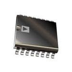
| 描述 | DGTL ISO 5KV RS422/RS485 16SOIC数字隔离器 5kV Sgnl Iso 16Mbps HiSpd Full/Hlf Duplx |
| 产品分类 | |
| 品牌 | Analog Devices Inc |
| 产品手册 | |
| 产品图片 |
|
| rohs | 符合RoHS无铅 / 符合限制有害物质指令(RoHS)规范要求 |
| 产品系列 | 接口 IC,数字隔离器,Analog Devices ADM2491EBRWZiCoupler® |
| 数据手册 | |
| 产品型号 | ADM2491EBRWZ |
| 上升/下降时间(典型值) | 20ns, 20ns (最小值) |
| 产品目录页面 | |
| 产品种类 | |
| 传播延迟tpLH/tpHL(最大值) | 60ns, 60ns |
| 供应商器件封装 | 16-SOIC |
| 共模瞬态抗扰度(最小值) | 25kV/µs |
| 关闭 | No Shutdown |
| 包装 | 管件 |
| 协议 | RS422,RS485 |
| 双工 | 全 |
| 商标 | Analog Devices |
| 安装类型 | 表面贴装 |
| 安装风格 | SMD/SMT |
| 封装 | Tube |
| 封装/外壳 | 16-SOIC(0.295",7.50mm 宽) |
| 封装/箱体 | SOIC-16 |
| 工作温度 | -40°C ~ 85°C |
| 工厂包装数量 | 47 |
| 技术 | 磁耦合 |
| 接收器滞后 | 30mV |
| 数据速率 | 16Mbps |
| 最大工作温度 | + 85 C |
| 最大数据速率 | 16 Mb/s |
| 最小工作温度 | - 40 C |
| 标准包装 | 47 |
| 电压-电源 | 3.3V,5V |
| 电压-隔离 | 5000Vrms |
| 电源电压-最大 | 5.5 V |
| 电源电压-最小 | 3 V |
| 电源电流 | 6 mA, 50 mA |
| 类型 | RS422, RS485 |
| 系列 | ADM2491E |
| 绝缘电压 | 5 kVrms |
| 脉宽失真(最大) | 7ns, 10ns |
| 输入-输入侧1/输入侧2 | 2/1 |
| 通道数 | 3 |
| 通道数量 | 3 Channel |
| 通道类型 | 单向 |
| 隔离式电源 | 是 |
| 驱动器/接收器数 | 1/1 |


- 商务部:美国ITC正式对集成电路等产品启动337调查
- 曝三星4nm工艺存在良率问题 高通将骁龙8 Gen1或转产台积电
- 太阳诱电将投资9.5亿元在常州建新厂生产MLCC 预计2023年完工
- 英特尔发布欧洲新工厂建设计划 深化IDM 2.0 战略
- 台积电先进制程称霸业界 有大客户加持明年业绩稳了
- 达到5530亿美元!SIA预计今年全球半导体销售额将创下新高
- 英特尔拟将自动驾驶子公司Mobileye上市 估值或超500亿美元
- 三星加码芯片和SET,合并消费电子和移动部门,撤换高东真等 CEO
- 三星电子宣布重大人事变动 还合并消费电子和移动部门
- 海关总署:前11个月进口集成电路产品价值2.52万亿元 增长14.8%


PDF Datasheet 数据手册内容提取
High Speed, ESD-Protected, Half-/Full-Duplex iCoupler Isolated RS-485 Transceiver Data Sheet ADM2491E FEATURES FUNCTIONAL BLOCK DIAGRAM Isolated, RS-485/RS-422 transceiver, configurable as half- or VDD1 VDD2 full-duplex ADM2491E ±8 kV ESD protection on RS-485 input/output pins DE 16 Mbps data rate N Complies with ANSI TIA/EIA RS-485-A-1998 and O TI Y ISO 8482: 1987(E) TxD OLA Suitable for 5 V or 3.3 V operation (VDD1) C IS Z High common-mode transient immunity: >25 kV/μs NI A V Receiver has open-circuit, fail-safe design L GA A 32 nodes on the bus RxD B Thermal shutdown protection RE Safety and regulatory approvals UL recognition: 5000 V rms isolation voltage GND1 GND2 06985-001 for 1 minute, per UL 1577 Figure 1. VDE certificate of conformity DIN V VDE V 0884-10 (VDE V 0884-10): 2006-12 Reinforced insulation, V = 849 V peak IORM Operating temperature range: −40°C to +85°C Wide body, 16-lead SOIC package APPLICATIONS Isolated RS-485/RS-422 interfaces Industrial field networks INTERBUS Multipoint data transmission systems GENERAL DESCRIPTION The ADM2491E is an isolated data transceiver with ±8 kV ESD The differential transmitter outputs and receiver inputs feature protection and is suitable for high speed, half- or full-duplex electrostatic discharge circuitry that provides protection to communication on multipoint transmission lines. For half- ±8 kV using the human body model (HBM). The logic side of duplex operation, the transmitter outputs and the receiver the device can be powered with either a 5 V or a 3.3 V supply, inputs share the same transmission line. Transmitter output whereas the bus side requires an isolated 5 V supply. Pin Y is linked externally to receiver input Pin A, and transmit- The device has current-limiting and thermal shutdown features ter output Pin Z is linked to receiver input Pin B. to protect against output short circuits and situations in which The ADM2491E is designed for balanced transmission lines bus contention could cause excessive power dissipation. and complies with ANSI TIA/EIA RS-485-A-1998 and ISO The ADM2491E is available in a wide body, 16-lead SOIC package 8482: 1987(E). The device employs Analog Devices, Inc., and operates over the −40°C to +85°C temperature range. iCoupler® technology to combine a 3-channel isolator, a three- state differential line driver, and a differential input receiver into a single package. Rev. C Document Feedback Information furnished by Analog Devices is believed to be accurate and reliable. However, no responsibility is assumed by Analog Devices for its use, nor for any infringements of patents or other One Technology Way, P.O. Box 9106, Norwood, MA 02062-9106, U.S.A. rights of third parties that may result from its use. Specifications subject to change without notice. No license is granted by implication or otherwise under any patent or patent rights of Analog Devices. Tel: 781.329.4700 ©2007–2014 Analog Devices, Inc. All rights reserved. Trademarks and registered trademarks are the property of their respective owners. Technical Support www.analog.com
ADM2491E Data Sheet TABLE OF CONTENTS Features .............................................................................................. 1 Switching Characteristics .................................................................9 Applications ....................................................................................... 1 Typical Performance Characteristics ........................................... 10 Functional Block Diagram .............................................................. 1 Circuit Description......................................................................... 12 General Description ......................................................................... 1 Electrical Isolation ...................................................................... 12 Revision History ............................................................................... 2 Truth Tables................................................................................. 12 Specifications ..................................................................................... 3 Thermal Shutdown .................................................................... 13 Timing Specifications .................................................................. 4 Fail-Safe Receiver Inputs ........................................................... 13 Package Characteristics ............................................................... 4 Magnetic Field Immunity .......................................................... 13 Regulatory Information ............................................................... 4 Applications Information .............................................................. 14 Insulation and Safety-Related Specifications ............................ 5 Isolated Power Supply Circuit .................................................. 14 VDE 0884 Insulation Characteristics ........................................ 5 PCB Layout ................................................................................. 14 Absolute Maximum Ratings ............................................................ 6 Typical Applications ................................................................... 15 ESD Caution .................................................................................. 6 Outline Dimensions ....................................................................... 16 Pin Configuration and Functional Descriptions .......................... 7 Ordering Guide .......................................................................... 16 Test Circuits ....................................................................................... 8 REVISION HISTORY 5/14—Rev. B to Rev. C Changed V from 848 V peak to 849 V peak (Throughout) . 1 IORM Changes to VDE 0884 Insulation Characteristics Conditions ... 5 Changes to Ordering Guide .......................................................... 16 12/10—Rev. A to Rev. B Changes to Figure 31 ...................................................................... 15 12/08—Rev. 0 to Rev. A Updated Regulatory Approval Status Throughout ...................... 1 Changes to Table 7 ............................................................................ 6 10/07—Revision 0: Initial Version Rev. C | Page 2 of 16
Data Sheet ADM2491E SPECIFICATIONS All voltages are relative to their respective ground; 3.0 V ≤ V ≤ 5.5 V, 4.5 V ≤ V ≤ 5.5 V. All minimum/maximum specifications DD1 DD2 apply over the entire recommended operation range, unless otherwise noted. All typical specifications are at T = 25°C, V = V = A DD1 DD2 5.0 V, unless otherwise noted. Table 1. Parameter Symbol Min Typ Max Unit Test Conditions SUPPLY CURRENT Power Supply Current, Logic Side TxD/RxD Data Rate = 2 Mbps I 3.0 mA Unloaded output DD1 TxD/RxD Data Rate = 16 Mbps I 6 mA Half-duplex configuration, DD1 R = 120 Ω, see Figure 5 TERMINATION Power Supply Current, Bus Side TxD/RxD Data Rate = 2 Mbps I 4.0 mA Unloaded output DD2 TxD/RxD Data Rate = 16 Mbps I 50 mA V = 5.5 V, half-duplex DD2 DD2 configuration, R = 120 Ω, see Figure 5 TERMINATION DRIVER Differential Outputs Differential Output Voltage, Loaded |V | 2.0 5.0 V R = 100 Ω (RS-422), see Figure 3 OD L 1.5 5.0 V R = 54 Ω (RS-485), see Figure 3 L 1.5 5.0 V −7 V ≤ V ≤ 12 V, see Figure 4 TEST1 ∆|V | for Complementary Output ∆|V | 0.2 V R = 54 Ω or 100 Ω, see Figure 3 OD OD L States Common-Mode Output Voltage V 3.0 V R = 54 Ω or 100 Ω, see Figure 3 OC L ∆|V | for Complementary Output ∆|V | 0.2 V R = 54 Ω or 100 Ω, see Figure 3 OC OC L States Output Leakage Current (Y, Z) I 100 μA DE = 0 V, V = 0 V or 5 V, V = 12 V O DD2 IN −100 μA DE = 0 V, V = 0 V or 5 V, V = −7 V DD2 IN Short-Circuit Output Current I 250 mA OS Logic Inputs DE, RE, TxD Input Threshold Low V 0.25 × V V IL DD1 Input Threshold High V 0.7 × V V IH DD1 Input Current I −10 +0.01 +10 μA TxD RECEIVER Differential Inputs Differential Input Threshold Voltage V −0.2 +0.2 V TH Input Voltage Hysteresis V 30 mV V = 0 V HYS OC Input Current (A, B) I +1.0 mA V = 12 V I OC −0.8 mA V = −7 V OC Line Input Resistance R 12 kΩ IN Logic Outputs Output Voltage Low V 0.2 0.4 V I = 1.5 mA, V − V = −0.2 V OLRxD ORxD A B Output Voltage High V V − 0.3 V − 0.2 V I = −1.5 mA, V − V = 0.2 V OHRxD DD1 DD1 ORxD A B Short-Circuit Current 100 mA Three-State Output Leakage Current I ±1 μA V = 5.5 V, 0 V < V < V OZR DD1 OUT DD1 COMMON-MODE TRANSIENT IMMUNITY1 25 kV/μs V = 1 kV, transient magnitude = CM 800 V 1 CM is the maximum common-mode voltage slew rate that can be sustained while maintaining specification-compliant operation. VCM is the common-mode potential difference between the logic and bus sides. The transient magnitude is the range over which the common mode is slewed. The common-mode voltage slew rates apply to both rising and falling common-mode voltage edges. Rev. C | Page 3 of 16
ADM2491E Data Sheet TIMING SPECIFICATIONS T = −40°C to +85°C. A Table 2. Parameter Symbol Min Typ Max Unit Test Conditions DRIVER Maximum Data Rate 16 Mbps Propagation Delay t , t 45 60 ns R = 54 Ω, C = C = 100 pF, PLH PHL L L1 L2 see Figure 6 and Figure 10 Pulse Width Distortion, t 7 ns R = 54 Ω, C = C = 100 pF, PWD L L1 L2 t = |t − t |, t = |t − t | see Figure 6 and Figure 10 PWD PYLH PYHL PWD PZLH PZHL Single-Ended Output Rise/Fall Times t, t 20 ns R = 54 Ω, C = C = 100 pF, R F L L1 L2 see Figure 6 and Figure 10 Enable Time 55 ns R = 110 Ω, C = 50 pF, see Figure 8 and L L Figure 11 Disable Time 55 ns R = 110 Ω, C = 50 pF, see Figure 8 and L L Figure 11 RECEIVER Propagation Delay t , t 60 ns C = 15 pF, see Figure 7 and Figure 12 PLH PHL L Pulse Width Distortion, t = |t − t | t 10 ns C = 15 pF, see Figure 7 and Figure 12 PWD PLH PHL PWD L Enable Time 13 ns R = 1 kΩ, C = 15 pF, see Figure 9 and L L Figure 13 Disable Time 13 ns R = 1 kΩ, C = 15 pF, see Figure 9 and L L Figure 13 PACKAGE CHARACTERISTICS Table 3. Parameter Symbol Min Typ Max Unit Test Conditions Resistance (Input to Output)1 R 1012 Ω I-O Capacitance (Input to Output)1 C 3 pF f = 1 MHz I-O Input Capacitance2 C 4 pF I Input IC Junction-to-Case Thermal Resistance θ 33 °C/W Thermocouple located at center JCI of package underside Output IC Junction-to-Case Thermal Resistance θ 28 °C/W JCO 1 Device considered a 2-terminal device: Pin 1, Pin 2, Pin 3, Pin 4, Pin 5, Pin 6, Pin 7, and Pin 8 are shorted together, and Pin 9, Pin 10, Pin 11, Pin 12, Pin 13, Pin 14, Pin 15, and Pin 16 are shorted together. 2 Input capacitance is from any input data pin to ground. REGULATORY INFORMATION Table 4. UL1 VDE2 Recognized under the 1577 component recognition program1 Certified according to DIN V VDE V 0884-10 (VDE V 0884-10): 2006-122 5000 V rms isolation voltage Reinforced insulation, 849 V peak 1 In accordance with UL 1577, each ADM2491E is proof tested by applying an insulation test voltage ≥ 6000 V rms for 1 second (current leakage detection limit = 10 μA). 2 In accordance with DIN V VDE V 0884-10, each ADM2491E is proof tested by applying an insulation test voltage ≥ 1590 V peak for 1 second (partial discharge detection limit = 5 pC). Rev. C | Page 4 of 16
Data Sheet ADM2491E INSULATION AND SAFETY-RELATED SPECIFICATIONS Table 5. Parameter Symbol Value Unit Conditions Rated Dielectric Insulation Voltage 5000 V rms 1 minute duration Minimum External Air Gap (Clearance) L(I01) 7.7 mm min Measured from input terminals to output terminals, shortest distance through air Minimum External Tracking (Creepage) L(I02) 8.1 mm min Measured from input terminals to output terminals, shortest distance along body Minimum Internal Gap (Internal Clearance) 0.017 mm min Insulation distance through insulation Tracking Resistance (Comparative Tracking Index) CTI >175 V DIN IEC 112/VDE 0303 Part 1 Isolation Group IIIa Material Group (DIN VDE 0110, 1/89) VDE 0884 INSULATION CHARACTERISTICS This isolator is suitable for reinforced electrical isolation only within the safety limit data. Maintenance of the safety data must be ensured by means of protective circuits. An asterisk (*) on a package denotes VDE 0884 approval for 849 V peak working voltage. Table 6. Description Symbol Characteristic Unit Installation Classification per DIN VDE 0110 for Rated Mains Voltage ≤300 V rms I to IV ≤450 V rms I to II ≤600 V rms I to II Climatic Classification 40/105/21 Pollution Degree (DIN VDE 0110, see Table 1) 2 Maximum Working Insulation Voltage V 849 V peak IORM Input-to-Output Test Voltage, Method b1 V 1590 V peak PR V × 1.875 = V , 100% Production Tested, t = 1 sec, Partial Discharge < 5 pC IORM PR m Input-to-Output Test Voltage, Method a V PR After Environmental Tests, Subgroup 1 1357 V peak V × 1.6 = V , t = 60 sec, Partial Discharge < 5 pC IORM PR m After Input and/or Safety Test, Subgroup 2/Subgroup 3 1018 V peak V × 1.2 = V , t = 60 sec, Partial Discharge < 5 pC IORM PR m Highest Allowable Overvoltage (Transient Overvoltage, t = 10 sec) V 6000 V peak TR TR Safety-Limiting Values (Maximum Value Allowed in the Event of a Failure, see Figure 20) Case Temperature T 150 °C S Input Current I 265 mA S, INPUT Output Current I 335 mA S, OUTPUT Insulation Resistance at T, V = 500 V R >109 Ω S IO S Rev. C | Page 5 of 16
ADM2491E Data Sheet ABSOLUTE MAXIMUM RATINGS T = 25 °C, unless otherwise noted. Each voltage is relative to its A Stresses above those listed under Absolute Maximum Ratings respective ground. may cause permanent damage to the device. This is a stress rating only; functional operation of the device at these or any Table 7. other conditions above those indicated in the operational Parameter Rating section of this specification is not implied. Exposure to absolute Storage Temperature −55°C to +150°C maximum rating conditions for extended periods may affect Ambient Operating Temperature −40°C to +85°C device reliability. V −0.5 V to +7 V DD1 V −0.5 V to +6 V Absolute maximum ratings apply individually only, not in DD2 Logic Input Voltages −0.5 V to V + 0.5 V combination. DD1 Bus Terminal Voltages −9 V to +14 V Logic Output Voltages −0.5 V to V + 0.5 V DD1 ESD CAUTION Average Output Current, per Pin ±35 mA ESD (Human Body Model) on A, B, Y, ±8 kV and Z Pins θ Thermal Impedance 60°C/W JA Rev. C | Page 6 of 16
Data Sheet ADM2491E PIN CONFIGURATION AND FUNCTIONAL DESCRIPTIONS VDD1 1 16 VDD2 GND1 2 15 GND2 RxD 3 ADM2491E 14 A RE 4 TOP VIEW 13 B DE 5 (Not to Scale) 12 Z TxD 6 11 Y NC 7 10 NC GND1 8NC = NO CONNECT9 GND2 06985-002 Figure 2. ADM2491E Pin Configuration Table 8. Pin Function Descriptions Pin No. Mnemonic Description 1 V Power Supply (Logic Side). Decoupling capacitor to GND required; capacitor value should be between DD1 1 0.01 μF and 0.1 μF. 2, 8 GND Ground (Logic Side). 1 3 RxD Receiver Output. 4 RE Receiver Enable Input. Active low logic input. When this pin is low, the receiver is enabled; when high, the receiver is disabled. 5 DE Driver Enable Input. Active high logic input. When this pin is high, the driver (transmitter) is enabled; when low, the driver is disabled. 6 TxD Transmit Data. 7, 10 NC No Connect. This pin must be left floating. 9, 15 GND Ground (Bus Side). 2 11 Y Driver Noninverting Output. 12 Z Driver Inverting Output. 13 B Receiver Inverting Input. 14 A Receiver Noninverting Input. 16 V Power Supply (Bus Side). Decoupling capacitor to GND is required; capacitor value should be between DD2 2 0.01 μF and 0.1 μF. Rev. C | Page 7 of 16
ADM2491E Data Sheet TEST CIRCUITS RL VOD 2 Y CL1 RL RLDIFF 2 VOC 06985-003 Z CL2 06985-006 Figure 3. Driver Voltage Measurement Figure 6. Driver Propagation Delay 375Ω A VOD 60Ω VTEST VOUT 375Ω 06985-004 B CL 06985-007 Figure 4. Driver Voltage Measurement Figure 7. Receiver Propagation Delay VDD1 VDD2 VOUT VCC Y ADM2491E RL 0V OR 3V S1 S2 DE TION Y DE Z CL 06985-008 A TxD OL Z RTERMINATION Figure 8. Driver Enable/Disable S C I NI A V L RxD GA AB +1.5V S1 VOUT VCC A RL RE –1.5V RE S2 GND1 GND2 06985-005 RE IN B CL 06985-009 Figure 5. Supply Current Measurement Test Circuit Figure 9. Receiver Enable/Disable Rev. C | Page 8 of 16
Data Sheet ADM2491E SWITCHING CHARACTERISTICS VDD1 TxD 1.5V 1.5V 0V A, B tPLH tPHL 0V 0V Z 1/2VOUT VOUT tPLH tPHL Y V OH tPWD = |tPLH –tPHL| VYVO,O HZL 10% P9O0%IN PTOINtTR t9F0% 1P0O%IN PTOINT 06985-010 RxD 1.5V 1.5V VOL 06985-012 Figure 10. Driver Propagation Delay, Rise/Fall Timing Figure 12. Receiver Propagation Delay VDD1 VDD1 DE 0.5VDD1 0.5VDD1 RE 0.5VDD1 0.5VDD1 0V 0V tZL tLZ tZL tLZ Y, Z 2.3V VOL + 0.5V RxD 1.5V OUTPUT LOW VOL + 0.5V VOL VOL tZH tHZ tZH OUTPUT HIGH tHZ VOH VOH Y, Z 2.3V VOH – 0.5V 0V 06985-011 Rx0DV 1.5V VOH – 0.5V 0V 06985-013 Figure 11. Driver Enable/Disable Delay Figure 13. Receiver Enable/Disable Delay Rev. C | Page 9 of 16
ADM2491E Data Sheet TYPICAL PERFORMANCE CHARACTERISTICS 2.58 60 NO LOAD 2.56 50 A) 2.54 m RENT ( 2.52 100Ω LOAD s) 40 ttPPLHHL Y CUR 2.50 LAY (n 30 PPL 2.48 DE SU 54ΩLOAD 20 DD1 2.46 I 10 2.44 2.42 0 –40 –20 0TEMPER20ATURE (°4C0) 60 80 06985-014 –40 –20 0TEMPER2A0TURE (°4C0) 60 80 06985-035 Figure 14. IDD1 Supply Current vs. Temperature Figure 17. Receiver Propagation Delay vs. Temperature 60 ∆: 2.12V @: 7.72V TxD 50 54ΩLOAD A) m T ( 40 N RE 100Ω LOAD 1 Z R CU 30 Y Y L P P SU 20 D2 3 RxD D I 10 NO LOAD 0–40 –20 0TEMPER2A0TURE (°4C0) 60 80 06985-015 4 CCHH13 22VV ΩΩ CCHH24 22VV ΩΩ MT 2 0 n s 48ns A CH1 2.32V 06985-032 Figure 15. IDD2 Supply Current vs. Temperature Figure 18. Driver/Receiver Propagation Delay, Low to High (RLDIFF = 54 Ω, CL1 = CL2 = 100 pF) 60 ∆: 2.12V tPZHL @: 7.72V t 50 PYLH t PZLH 40 TxD ns) tPYHL 1 Y ( 30 Z A L E D Y 20 3 10 0–40 –20 0TEMPER2A0TURE (°4C0) 60 80 06985-034 4 CCHH13 22VV ΩΩ CCHH24 22VV ΩΩ MT 2 0 n s 48ns AR xCDH1 3.24V 06985-033 Figure 16. Driver Propagation Delay vs. Temperature Figure 19. Driver/Receiver Propagation Delay, High to Low (RLDIFF = 54 Ω, CL1 = CL2 = 100 pF) Rev. C | Page 10 of 16
Data Sheet ADM2491E 350 4.76 4.75 300 A) 4.74 m T ( 250 4.73 N RE SIDE 2 4.72 CUR 200 E (V)4.71 G G N A TI 150 LT4.70 MI O LI SIDE 1 V4.69 ETY- 100 4.68 F A S 4.67 50 4.66 00 50CASE TEMP1E0R0ATURE (°C) 150 200 06985-020 4.65–40 –20 0TEMPER2A0TURE (°4C0) 60 80 06985-036 Figure 20. Thermal Derating Curve, Dependence of Safety-Limiting Values Figure 23. Receiver Output High Voltage vs. Temperature, with Case Temperature per VDE 0884 IRxD = −4 mA 0 0.35 –2 0.30 mA) –4 0.25 RENT ( –6 E (V) 0.20 R G U A UT C –8 OLT 0.15 P V T OU–10 0.10 –12 0.05 –144.0 4.2RECEIVE4R. 4OUTPUT V4O.6LTAGE (V)4.8 5.0 06985-021 0–40 –20 0TEMPER2A0TURE (°4C0) 60 80 06985-037 Figure 21. Output Current vs. Receiver Output High Voltage Figure 24. Receiver Output Low Voltage vs. Temperature, IRxD = –4 mA 16 14 A) m T ( 12 N E R 10 R U C T 8 U P T OU 6 4 2 0 0 0.2 RECE0I.V4ER OUT0P.6UT VOLTA0.G8E (V) 1.0 1.2 06985-022 Figure 22. Output Current vs. Receiver Output Low Voltage Rev. C | Page 11 of 16
ADM2491E Data Sheet CIRCUIT DESCRIPTION ELECTRICAL ISOLATION TRUTH TABLES In the ADM2491E, electrical isolation is implemented on the The truth tables in this section use the abbreviations shown in logic side of the interface. Therefore, the part has two main Table 9. sections: a digital isolation section and a transceiver section (see Figure 25). The driver input signal, which is applied to the Table 9. Truth Table Abbreviations TxD pin and referenced to logic ground (GND), is coupled Letter Description 1 across an isolation barrier to appear at the transceiver section H High level referenced to isolated ground (GND). Similarly, the receiver L Low level 2 input, which is referenced to isolated ground in the transceiver I Indeterminate section, is coupled across the isolation barrier to appear at the X Irrelevant RxD pin referenced to logic ground. Z High impedance (off) NC Disconnected iCoupler Technology The digital signals are transmitted across the isolation barrier using iCoupler technology. This technique uses chip scale Table 10. Transmitting transformer windings to couple the digital signals magnetically Supply Status Inputs Outputs from one side of the barrier to the other. Digital inputs are V V DE TxD Y Z encoded into waveforms that are capable of exciting the DD1 DD2 On On H H H L primary transformer winding. At the secondary winding, the On On H L L H induced waveforms are decoded into the binary value that was On On L X Z Z originally transmitted. On Off X X Z Z VDD1 VDD2 Off On L L Z Z Off Off X X Z Z ISOLATION BARRIER DE ENCODE DECODE Table 11. Receiving Supply Status Inputs Output Y VDD1 VDD2 A − B (V) RE RxD TxD ENCODE DECODE D Z On On >0.2 L or NC H On On <−0.2 L or NC L A On On −0.2 < A − B < +0.2 L or NC I RxD DECODE ENCODE R B On On Inputs open L or NC H RE On On X H Z DIGITAL ISOLATION TRANSCEIVER GND1 GND2 06985-025 OOnff OOffff XX LL oorr NNCC HL Figure 25. ADM2491E Digital Isolation and Transceiver Sections Rev. C | Page 12 of 16
Data Sheet ADM2491E 100 THERMAL SHUTDOWN The ADM2491E contains thermal shutdown circuitry that C protects the part from excessive power dissipation during fault ETI 10 csoounrdcieti ocnans. rSehsourltt iinng h tihgeh d drriviveerr o cuutrpruetnst sto. T ah leo wth iemrmpeadl asenncsei ng E MAGNGAUSS) 1 Lk ccdooifer ns1cidu5g0iintt°ireCoydn dit soae nr tdeedaci stcdashib stelhadebe .t l Ahienses c tdrthhereaie vs ddeerr eii vvnoeiu cdrte ipo ecuu ottteospm luwspt,h ste.eh rTnae th adui rsrdi eciv eiuer rtncesud maietrprre yet hr iaisst u re MUMALLOWABFLUX DENSITY ( 0.1 re-enabled at a temperature of 140°C. AXI 0.01 M FAIL-SAFE RECEIVER INPUTS Tlohgeic r hecigehiv eorn i nthpeu Rtsx iDnc pluind ew ah feanil t-hsaef eA f aeantdu rBe itnhpaut tgsu aarrea fnltoeaetsi nag 0.0011k 10kMAGNETI1C0 F0kIELD FREQ1MUENCY (Hz1)0M 100M 06985-026 Figure 26. Maximum Allowable External Magnetic Flux Density or open circuited. For example, at a magnetic field frequency of 1 MHz, the MAGNETIC FIELD IMMUNITY maximum allowable magnetic field of 0.2 kgauss induces a Because iCoupler devices use a coreless technology, no magnetic voltage of 0.25 V at the receiving coil. This is about 50% of the components are present and the problem of magnetic saturation sensing threshold and does not cause a faulty output transition. of the core material does not exist. Therefore, iCoupler devices Similarly, if such an event occurs during a transmitted pulse and have essentially infinite dc field immunity. The following analysis is the worst-case polarity, it reduces the received pulse from defines the conditions under which this may occur. The 3 V >1.0 V to 0.75 V—still well above the 0.5 V sensing threshold of operating condition of the ADM2491E is examined because it the decoder. represents the most susceptible mode of operation. Figure 27 shows the magnetic flux density values in terms of The limitation on the ac magnetic field immunity of the iCoupler more familiar quantities, such as maximum allowable current is set by the condition that induced an error voltage in the flow, at given distances away from the ADM2491E transformers. receiving coil (the bottom coil in this case) that was large to 1000 either falsely set or reset the decoder. The voltage induced across the bottom coil is given by A) DISTANCE = 1m T (k 100 V dβrn2 ; n1,2,...,N RREN DISTANCE = 5mm dt U C 10 E where (if the pulses at the transformer output are greater than BL 1.0 V in amplitude): WA DISTANCE = 100mm O 1 L β is the magnetic flux density (gauss). L A N is the number of turns in the receiving coil. UM rn is the radius of the nth turn in the receiving coil (cm). AXIM 0.1 M The decoder has a sensing threshold of about 0.5 V; therefore, ttohleerrea tise da. 0 .5 V margin in which induced voltages can be 0.011k 10kMAGNETI1C0 F0kIELD FREQ1MUENCY (Hz1)0M 100M 06985-027 Figure 27. Maximum Allowable Current for Given the geometry of the receiving coil and an imposed Various Current-to-ADM2491E Spacings requirement that the induced voltage is, at most, 50% of the With combinations of strong magnetic field and high frequency, 0.5 V margin at the decoder, a maximum allowable magnetic any loops formed by printed circuit board traces can induce field is calculated, as shown in Figure 26. error voltages large enough to trigger the thresholds of succeeding circuitry. Care should be taken in the layout of such traces to avoid this possibility. Rev. C | Page 13 of 16
ADM2491E Data Sheet APPLICATIONS INFORMATION ISOLATED POWER SUPPLY CIRCUIT PCB LAYOUT The ADM2491E requires isolated power capable of 5 V at up to The ADM2491E isolated RS-485 transceiver requires no external approximately 75 mA (this current is dependent on the data interface circuitry for the logic interfaces. Power supply bypass- rate and termination resistors used) to be supplied between the ing is required at the input and output supply pins (see Figure 29). V and the GND pins. A transformer driver circuit with a Bypass capacitors are conveniently connected between Pin 1 DD2 2 center-tapped transformer and LDO can be used to generate the and Pin 2 for V and between Pin 15 and Pin 16 for V . The DD1 DD2 isolated 5 V supply, as shown in Figure 28. The center-tapped capacitor value should be between 0.01 μF and 0.1 μF. The total transformer provides electrical isolation of the 5 V power lead length between both ends of the capacitor and the input supply. The primary winding of the transformer is excited with power supply pin should not exceed 20 mm. Bypassing between a pair of square waveforms that are 180° out of phase with each Pin 1 and Pin 8 and between Pin 9 and Pin 16 should also be other. A pair of Schottky diodes and a smoothing capacitor are considered unless the ground pair on each package side is used to create a rectified signal from the secondary winding. connected close to the package. The ADP3330 linear voltage regulator provides a regulated power supply to the bus-side circuitry (V ) of the VDD1 VDD2 DD2 GND1 GND2 ADM2491E. RxD A RE ADM2491E B ISOLATION DE Z VCC BARRIER TxD Y NC NC SD103C +22µF ISND ADP33O3U0T 5V+10µF GNFDig1ure 29. RecomNmCe =n dNeOd C POriNnNteEdC TCircuit Board LGaNyDou2t 06985-029 TRANSFORMER VCC ERR DRIVER NR In applications involving high common-mode transients, care GND should be taken to ensure that board coupling across the isola- 78253 SD103C tion barrier is minimized. Furthermore, the board layout should VCC be designed such that any coupling that does occur equally affects all pins on a given component side. Failure to ensure this could VDD1 VDD2 cause voltage differentials between pins exceeding the absolute maximum ratings of the device, thereby leading to latch-up or ADM2491E permanent damage. GND1 GND2 06985-028 Figure 28. Isolated Power Supply Circuit Rev. C | Page 14 of 16
Data Sheet ADM2491E TYPICAL APPLICATIONS at the receiving end in its characteristic impedance, and stub lengths off the main line must be kept as short as possible. For Figure 30 and Figure 31 show typical applications of the half-duplex operation, this means that both ends of the line ADM2491E in half-duplex and full-duplex RS-485 network must be terminated because either end can be the receiving end. configurations. Up to 32 transceivers can be connected to the RS-485 bus. To minimize reflections, the line must be terminated VCC MAXIMUM NUMBER OF TRANSCEIVERS ON BUS = 32 ADM2491E ADM2491E A R1 A RxD R B B R RxD RE RE RT RT DE DE Z Z TxD D Y R2 Y D TxD A B Z Y A B Z Y R R D D ADM2491E ADM2491E RxD RE DE TxD RxDRE DE TxD N1.O RTTE ISS EQUAL TO THE CHARACTERISTIC IMPEDANCE OF THE CABLE. 06985-030 2. ISOLATION NOT SHOWN. Figure 30. ADM2491E Typical Half-Duplex RS-485 Network MAXIMUMNUMBEROFNODES=32 MASTER VDD SLAVE R1 A Y RxD R B RT Z D TxD RE DE DE Z R2 R2 B RE TxD D Y RT A R RxD VDDR1 ADM2491E ADM2491E A B Z Y A B Z Y SLAVE SLAVE R R D D ADM2491E ADM2491E RxD RE DE TxD RxD RE DE TxD N1.ORTTEISSEQUALTOTHECHARACTERISTICIMPEDANCEOFTHECABLE. 06985-031 Figure 31. ADM2491E Typical Full -Duplex RS-485 Network Rev. C | Page 15 of 16
ADM2491E Data Sheet OUTLINE DIMENSIONS 10.50(0.4134) 10.10(0.3976) 16 9 7.60(0.2992) 7.40(0.2913) 1 10.65(0.4193) 8 10.00(0.3937) 1.27(0.0500) 0.75(0.0295) BSC 2.65(0.1043) 0.25(0.0098) 45° 0.30(0.0118) 2.35(0.0925) 8° 0.10(0.0039) 0° COPLANARITY 0.10 0.51(0.0201) SPELAATNIENG 0.33(0.0130) 1.27(0.0500) 0.31(0.0122) 0.20(0.0079) 0.40(0.0157) C(RINOEFNPEATRRREOENNLCLTEIHNCEOGOSNDMELISPYM)LAEAIANNRNDSETIOARTRNOOESUJNANEORDDETEEDAICN-POSMPFTRIFALONLMPIDMIRLAELIRATIMTDEEESRTFSMEO;SRIRN-0ECU1QH3SU-EADIVAIINMAELDENENSSTIIOGSNNFS.OR 03-27-2007-B Figure 32. 16-Lead Standard Small Outline Package [SOIC_W] Wide Body (RW-16) Dimensions shown in millimeters and (inches) ORDERING GUIDE Model1 Temperature Range Package Description Package Option ADM2491EBRWZ −40°C to +85°C 16-Lead Standard Small Outline Package, Wide Body [SOIC_W] RW-16 ADM2491EBRWZ–REEL7 −40°C to +85°C 16-Lead Standard Small Outline Package, Wide Body [SOIC_W] RW-16 EVAL-ADM2491EEBZ Evaluation Board 1 Z = RoHS Compliant Part. ©2007–2014 Analog Devices, Inc. All rights reserved. Trademarks and registered trademarks are the property of their respective owners. D06985-0-5/14(C) Rev. C | Page 16 of 16
Mouser Electronics Authorized Distributor Click to View Pricing, Inventory, Delivery & Lifecycle Information: A nalog Devices Inc.: ADM2491EBRWZ EVAL-ADM2491EEBZ ADM2491EBRWZ-REEL7