
 Datasheet下载
- 型号: ADM2490EBRWZ
- 制造商: Analog
- 库位|库存: xxxx|xxxx
- 要求:
| 数量阶梯 | 香港交货 | 国内含税 |
| +xxxx | $xxxx | ¥xxxx |
查看当月历史价格
查看今年历史价格
ADM2490EBRWZ产品简介:
ICGOO电子元器件商城为您提供ADM2490EBRWZ由Analog设计生产,在icgoo商城现货销售,并且可以通过原厂、代理商等渠道进行代购。 ADM2490EBRWZ价格参考。AnalogADM2490EBRWZ封装/规格:数字隔离器, RS422,RS485 数字隔离器 5000Vrms 2 通道 16Mbps 25kV/µs CMTI 16-SOIC(0.295",7.50mm 宽)。您可以下载ADM2490EBRWZ参考资料、Datasheet数据手册功能说明书,资料中有ADM2490EBRWZ 详细功能的应用电路图电压和使用方法及教程。
ADM2490EBRWZ 是由 Analog Devices Inc.(亚德诺半导体)生产的一款数字隔离器,属于 iCoupler 系列。它是一款高度集成的隔离式 RS-485/RS-422 收发器,广泛应用于需要电气隔离和高效数据传输的工业及通信领域。

 应用场景:

1. 工业自动化与控制
   ADM2490EBRWZ 适用于工业现场总线通信,例如 PLC(可编程逻辑控制器)、DCS(分布式控制系统)和远程 I/O 模块之间的数据交换。其高共模瞬变抗扰度和强大的电气隔离能力,确保在恶劣工业环境中可靠运行。

2. 楼宇自动化系统
   在楼宇自动化中,该器件可用于 HVAC(暖通空调)、照明控制和安防监控系统的通信链路。通过 RS-485 接口实现设备间的长距离、低功耗通信。

3. 电机驱动与逆变器控制
   用于电机驱动器和逆变器的通信接口,提供信号隔离以防止高压噪声干扰主控电路。其快速传播延迟和低脉宽失真特性,有助于提高系统的实时性和稳定性。

4. 医疗设备
   在医疗设备中,如监护仪、超声波设备或诊断仪器,该器件可以实现患者端与主机之间的安全隔离,同时保持精确的数据传输。

5. 电力能源管理
   适用于智能电网中的电表读取、配电自动化和能量管理系统。其 ±15kV ESD 保护功能增强了在复杂电磁环境下的可靠性。

6. 汽车电子
   在汽车应用中,如 CAN 至 RS-485 转换器或车载网络模块,ADM2490EBRWZ 提供了可靠的电气隔离,避免不同地电位引起的损坏。

7. 通信基础设施
   用于基站、路由器或其他通信设备中的数据链路隔离,支持多点通信网络并减少电磁干扰影响。

总结来说,ADM2490EBRWZ 的高性能隔离特性和坚固设计使其成为各种对安全性、可靠性和效率要求较高的应用场景的理想选择。
| 参数 | 数值 |
| 产品目录 | 集成电路 (IC)半导体 |
| 描述 | IC TXRX RS-485 ISOLATED 16-SOIC数字隔离器 5kV Sgnl Iso Hi Spd 16Mbps Full Duplex |
| 产品分类 | |
| 品牌 | Analog Devices |
| 产品手册 | |
| 产品图片 |
|
| rohs | 符合RoHS无铅 / 符合限制有害物质指令(RoHS)规范要求 |
| 产品系列 | 接口 IC,数字隔离器,Analog Devices ADM2490EBRWZiCoupler® |
| 数据手册 | |
| 产品型号 | ADM2490EBRWZ |
| 产品培训模块 | http://www.digikey.cn/PTM/IndividualPTM.page?site=cn&lang=zhs&ptm=25559 |
| 产品目录页面 | |
| 产品种类 | |
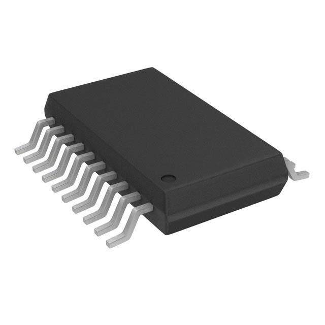
| 供应商器件封装 | 16-SOIC |
| 关闭 | No Shutdown |
| 包装 | 管件 |
| 协议 | RS422,RS485 |
| 双工 | 全 |
| 商标 | Analog Devices |
| 安装类型 | 表面贴装 |
| 安装风格 | SMD/SMT |
| 封装 | Tube |
| 封装/外壳 | 16-SOIC(0.295",7.50mm 宽) |
| 封装/箱体 | SOIC-16 |
| 工作温度 | -40°C ~ 105°C |
| 工厂包装数量 | 47 |
| 接收器滞后 | 70mV |
| 数据速率 | 16Mbps |
| 最大工作温度 | + 105 C |
| 最大数据速率 | 16 Mb/s |
| 最小工作温度 | - 40 C |
| 标准包装 | 47 |
| 电压-电源 | 3V,5V |
| 电源电压-最大 | 5.5 V |
| 电源电压-最小 | 2.7 V |
| 电源电流 | 4 mA |
| 类型 | RS-485 |
| 系列 | ADM2490E |
| 绝缘电压 | 5 kVrms |
| 视频文件 | http://www.digikey.cn/classic/video.aspx?PlayerID=1364138032001&width=640&height=505&videoID=2219593469001http://www.digikey.cn/classic/video.aspx?PlayerID=1364138032001&width=640&height=505&videoID=2219593470001http://www.digikey.cn/classic/video.aspx?PlayerID=1364138032001&width=640&height=505&videoID=2219614223001 |
| 通道数量 | 2 Channel |
| 驱动器/接收器数 | 1/1 |


- 商务部:美国ITC正式对集成电路等产品启动337调查
- 曝三星4nm工艺存在良率问题 高通将骁龙8 Gen1或转产台积电
- 太阳诱电将投资9.5亿元在常州建新厂生产MLCC 预计2023年完工
- 英特尔发布欧洲新工厂建设计划 深化IDM 2.0 战略
- 台积电先进制程称霸业界 有大客户加持明年业绩稳了
- 达到5530亿美元!SIA预计今年全球半导体销售额将创下新高
- 英特尔拟将自动驾驶子公司Mobileye上市 估值或超500亿美元
- 三星加码芯片和SET,合并消费电子和移动部门,撤换高东真等 CEO
- 三星电子宣布重大人事变动 还合并消费电子和移动部门
- 海关总署:前11个月进口集成电路产品价值2.52万亿元 增长14.8%


PDF Datasheet 数据手册内容提取
High Speed, ESD-Protected, Full-Duplex, iCoupler Isolated RS-485 Transceiver ADM2490E FEATURES FUNCTIONAL BLOCK DIAGRAM Isolated, full-duplex RS-485/RS-422 transceiver VDD1 VDD2 ±8 kV ESD protection on RS-485 input/output pins ADM2490E 16 Mbps data rate Complies with ANSI TIA/EIA-485-A-1998 and ISO 8482: 1987(E) ON Y TxD TI Suitable for 5 V or 3 V operation (V ) A Z DD1 L O High common-mode transient immunity: >25 kV/μs S C I Receiver has open-circuit, fail-safe design NI 32 nodes on the bus LVA A RxD A Thermal shutdown protection G B Safety and regulatory approvals ULf orerc 1o mgninituioten :p 5e0r0 U0L V 1 r5m77s isolation voltage GND1 GND2 05889-001 Figure 1. VDE certificate of conformity DIN EN 60747-5-2 (VDE 0884-10 Part 2): 2003-01 DIN EN 60950 (VDE 0805): 2001-12; EN 60950: 2000 V = 848 V peak IORM Operating temperature range: −40°C to +105°C Wide body, 16-lead SOIC package APPLICATIONS Isolated RS-485/RS-422 interfaces Industrial field networks INTERBUS Multipoint data transmission systems GENERAL DESCRIPTION The ADM2490E is an isolated data transceiver with ±8 kV ESD using the human body model (HBM). The logic side of the device protection that is suitable for high speed, full-duplex communi- can be powered with either a 5 V or a 3 V supply, whereas the cation on multipoint transmission lines. It is designed for balanced bus side requires an isolated 5 V supply. transmission lines and complies with ANSI TIA/EIA-485-A-1998 The device has current-limiting and thermal shutdown features and ISO 8482: 1987(E). The device employs Analog Devices, Inc., to protect against output short circuits and situations where bus iCoupler® technology to combine a 2-channel isolator, a three- contention could cause excessive power dissipation. state differential line driver, and a differential input receiver into The ADM2490E is available in a wide body, 16-lead SOIC package a single package. and operates over the −40°C to +105°C temperature range. The differential transmitter outputs and receiver inputs feature electrostatic discharge circuitry that provides protection to ±8 kV Rev. A Information furnished by Analog Devices is believed to be accurate and reliable. However, no responsibility is assumed by Analog Devices for its use, nor for any infringements of patents or other One Technology Way, P.O. Box 9106, Norwood, MA 02062-9106, U.S.A. rights of third parties that may result from its use. Specifications subject to change without notice. No license is granted by implication or otherwise under any patent or patent rights of Analog Devices. Tel: 781.329.4700 www.analog.com Trademarks and registered trademarks are the property of their respective owners. Fax: 781.461.3113 ©2006–2008 Analog Devices, Inc. All rights reserved.
ADM2490E TABLE OF CONTENTS Features .............................................................................................. 1 Switching Characteristics .................................................................9 Applications ....................................................................................... 1 Typical Performance Characteristics ........................................... 10 Functional Block Diagram .............................................................. 1 Circuit Description......................................................................... 12 General Description ......................................................................... 1 Electrical Isolation ...................................................................... 12 Revision History ............................................................................... 2 Truth Tables................................................................................. 12 Specifications ..................................................................................... 3 Thermal Shutdown .................................................................... 13 Timing Specifications .................................................................. 4 Fail-Safe Receiver Inputs ........................................................... 13 Package Characteristics ............................................................... 4 Magnetic Field Immunity .......................................................... 13 Regulatory Information ............................................................... 5 Applications Information .............................................................. 14 Insulation and Safety-Related Specifications ............................ 5 Isolated Power Supply Circuit .................................................. 14 VDE 0884-10 Insulation Characteristics ................................... 5 PCB Layout ................................................................................. 14 Absolute Maximum Ratings ............................................................ 6 Typical Applications ................................................................... 15 ESD Caution .................................................................................. 6 Outline Dimensions ....................................................................... 16 Pin Configuration and Function Descriptions ............................. 7 Ordering Guide .......................................................................... 16 Test Circuits ....................................................................................... 8 REVISION HISTORY 8/08—Rev. 0 to Rev. A Changes to Regulatory Approval Status Throughout .................. 1 Changed VDE 0884 to VDE 0884-10 Throughout ...................... 1 Changes to Table 5 ............................................................................ 5 Changes to Table 8 ............................................................................ 6 Changes to Figure 9 .......................................................................... 9 Changes to iCoupler Technology Section ................................... 12 Changes to Magnetic Field Immunity Section ........................... 13 Changes to Isolated Power Supply Circuit Section .................... 14 Changes to Figure 25 ...................................................................... 14 Added Typical Applications Section ............................................ 15 Updated Outline Dimensions ....................................................... 16 Changes to Ordering Guide .......................................................... 16 10/06—Revision 0: Initial Version Rev. A | Page 2 of 16
ADM2490E SPECIFICATIONS All voltages are relative to their respective ground; 2.7 ≤ V ≤ 5.5 V, 4.5 V ≤ V ≤ 5.5 V. All minimum/maximum specifications apply DD1 DD2 over the entire recommended operation range, unless otherwise noted. All typical specifications are at T = 25°C, V = V = 5.0 V, A DD1 DD2 unless otherwise noted. Table 1. Parameter Symbol Min Typ Max Unit Test Conditions SUPPLY CURRENT Power Supply Current, Logic Side TxD/RxD Data Rate < 2 Mbps I 3.0 mA 2.7 V ≤ V ≤ 5.5 V, unloaded DD1 DD1 TxD/RxD Data Rate = 16 Mbps I 6 mA 100 Ω load between Y and Z DD1 Power Supply Current, Bus Side TxD/RxD Data Rate < 2 Mbps I 4.0 mA 2.7 V ≤ V ≤ 5.5 V, unloaded DD2 DD1 TxD/RxD Data Rate = 16 Mbps I 60 mA 100 Ω load between Y and Z DD2 DRIVER Differential Outputs Differential Output Voltage, Loaded |V | 2.0 5.0 V R = 50 Ω (RS-422), see Figure 3 OD2 L 1.5 5.0 V R = 27 Ω (RS-485), see Figure 3 L |V | 1.5 5.0 V −7 V ≤ V ≤ +12 V, see Figure 4 OD4 TEST1 ∆|V | for Complementary Output States ∆|V | 0.2 V R = 54 Ω or 100 Ω, see Figure 3 OD OD L Common-Mode Output Voltage V 3.0 V R = 54 Ω or 100 Ω, see Figure 3 OC L ∆|V | for Complementary Output States ∆|V | 0.2 V R = 54 Ω or 100 Ω, see Figure 3 OC OC L Short-Circuit Output Current I 200 mA OS Logic Inputs Input Threshold Low V 0.25 × V V IL DD1 Input Threshold High V 0.7 × V V IH DD1 TxD Input Current I −10 +0.01 +10 μA TxD RECEIVER Differential Inputs Differential Input Threshold Voltage V −0.2 +0.2 V TH Input Voltage Hysteresis V 70 mV V = 0 V HYS OC Input Current (A, B) I 1.0 mA V = 12 V I OC −0.8 mA V = −7 V OC Line Input Resistance R 12 kΩ IN Logic Outputs Output Voltage Low V 0.2 0.4 V I = 1.5 mA, V − V = −0.2 V OLRxD ORxD A B Output Voltage High V V − 0.3 V − 0.2 V I = −1.5 mA, V − V = 0.2 V OHRxD DD1 DD1 ORxD A B Short-Circuit Current 100 mA COMMON-MODE TRANSIENT IMMUNITY1 25 kV/μs V = 1 kV, transient CM magnitude = 800 V 1 CM is the maximum common-mode voltage slew rate that can be sustained while maintaining specification-compliant operation. VCM is the common-mode potential difference between the logic and bus sides. The transient magnitude is the range over which the common-mode is slewed. The common-mode voltage slew rates apply to both rising and falling common-mode voltage edges. Rev. A | Page 3 of 16
ADM2490E TIMING SPECIFICATIONS T = −40°C to +85°C. A Table 2. Parameter Symbol Min Typ Max Unit Test Conditions DRIVER Maximum Data Rate 16 Mbps Propagation Delay t , t 45 60 ns R = 54 Ω, C = C = 100 pF, PLH PHL L L1 L2 see Figure 6 and Figure 8 Pulse Width Distortion, t , t 7 ns R = 54 Ω, C = C = 100 pF, PWD PWD L L1 L2 PWD = |t − t |, PWD = |t − t | see Figure 6 and Figure 8 PYLH PYHL PZLH PZHL Single-Ended Output Rise/Fall Times t, t 20 ns R = 54 Ω, C = C = 100 pF, R F L L1 L2 see Figure 6 and Figure 8 RECEIVER Propagation Delay t , t 60 ns C = 15 pF, see Figure 7 and Figure 9 PLH PHL L Pulse Width Distortion, PWD = |t − t | t 10 ns C = 15 pF, see Figure 7 and Figure 9 PLH PHL PWD L T = −40°C to +105°C. A Table 3. Parameter Symbol Min Typ Max Unit Test Conditions DRIVER Maximum Data Rate 10 Mbps Propagation Delay t , t , 45 60 ns R = 54 Ω, C = C = 100 pF, PYLH PYHL L L1 L2 t , t see Figure 6 and Figure 8 PZLH PZHL Pulse Width Distortion, t , t 9 ns R = 54 Ω, C = C = 100 pF, PWD PWD L L1 L2 PWD = |t − t |, PWD = |t − t | see Figure 6 and Figure 8 PYLH PYHL PZLH PZHL Single-Ended Output Rise/Fall Time t, t 27 ns R = 54 Ω, C = C = 100 pF, R F L L1 L2 see Figure 6 and Figure 8 RECEIVER Propagation Delay t , t 60 ns C = 15 pF, see Figure 7 and PLH PHL L Figure 9 Pulse Width Distortion, PWD = |t − t | t 10 ns C = 15 pF, see Figure 7 and PLH PHL PWD L Figure 9 PACKAGE CHARACTERISTICS Table 4. Parameter Symbol Min Typ Max Unit Test Conditions Resistance (Input to Output)1 R 1012 Ω I-O Capacitance (Input to Output)1 C 3 pF f = 1 MHz I-O Input Capacitance2 C 4 pF I Input IC Junction-to-Case Thermal Resistance θ 33 °C/W Thermocouple located at center JCI of package underside Output IC Junction-to-Case Thermal Resistance θ 28 °C/W JCO 1 Device considered a 2-terminal device: Pin 1, Pin 2, Pin 3, Pin 4, Pin 5, Pin 6, Pin 7, and Pin 8 are shorted together and Pin 9, Pin 10, Pin 11, Pin 12, Pin 13, Pin 14, Pin 15, and Pin 16 are shorted together. 2 Input capacitance is from any input data pin to ground. Rev. A | Page 4 of 16
ADM2490E REGULATORY INFORMATION Table 5. ADM2490E Approvals Organization Approval Type Notes UL Recognized under the Component Recognition In accordance with UL 1577, each ADM2490E is proof tested by Program of Underwriters Laboratories, Inc. applying an insulation test voltage ≥ 6000 V rms for 1 second (current leakage detection limit = 10 μA). VDE Certified according to DIN EN 60747-5-2 In accordance with DIN EN 60747-5-2, each ADM2490E is proof (VDE 0884-10 Part 2): 2003-01, tested by applying an insulation test voltage ≥ 1590 V peak for DIN EN 60950 (VDE 0805): 2001-12; EN 60950: 2000 1 second (partial discharge detection limit = 5 pC). INSULATION AND SAFETY-RELATED SPECIFICATIONS Table 6. Parameter Symbol Value Unit Conditions Rated Dielectric Insulation Voltage 5000 V rms 1 minute duration Minimum External Air Gap (Clearance) L(I01) 7.45 mm min Measured from input terminals to output terminals, shortest distance through air Minimum External Tracking (Creepage) L(I02) 8.1 mm min Measured from input terminals to output terminals, shortest distance along body Minimum Internal Gap (Internal Clearance) 0.017 mm min Insulation distance through insulation Tracking Resistance (Comparative Tracking Index) CTI >175 V DIN IEC 112/VDE 0303 Part 1 Isolation Group IIIa Material Group (DIN VDE 0110, 1/89) VDE 0884-10 INSULATION CHARACTERISTICS This isolator is suitable for basic electrical isolation only within the safety limit data. Maintenance of the safety data must be ensured by means of protective circuits. An asterisk (*) on a package denotes VDE 0884-10 approval for 848 V peak working voltage. Table 7. Description Symbol Characteristic Unit Installation Classification per DIN VDE 0110 for Rated Mains Voltage ≤300 V rms I to IV ≤450 V rms I to II ≤600 V rms I to II Climatic Classification 40/105/21 Pollution Degree (DIN VDE 0110, see Table 1) 2 Maximum Working Insulation Voltage V 848 V peak IORM Input-to-Output Test Voltage, Method b1 V 1590 V peak PR V × 1.875 = V , 100% Production Tested, t = 1 sec, Partial Discharge < 5 pC IORM PR m Input-to-Output Test Voltage, Method a After Environmental Tests, Subgroup 1 V × 1.6 = V , t = 60 sec, Partial Discharge < 5 pC 1357 V peak IORM PR m After Input and/or Safety Test, Subgroup 2/3 V × 1.2 = V , t = 60 sec, Partial Discharge < 5 pC V 1018 V peak IORM PR m PR Highest Allowable Overvoltage (Transient Overvoltage, t = 10 sec) V 6000 V peak TR TR Safety-Limiting Values (Maximum Value Allowed in the Event of a Failure; see Figure 16) Case Temperature T 150 °C S Input Current I 265 mA S, INPUT Output Current I 335 mA S, OUTPUT Insulation Resistance at T, V = 500 V R >109 Ω S IO S Rev. A | Page 5 of 16
ADM2490E ABSOLUTE MAXIMUM RATINGS T = 25°C, unless otherwise noted. Each voltage is relative to its A Stresses above those listed under Absolute Maximum Ratings respective ground. may cause permanent damage to the device. This is a stress rating only; functional operation of the device at these or any Table 8. other conditions above those indicated in the operational Parameter Rating section of this specification is not implied. Exposure to absolute Storage Temperature Range −55°C to +150°C maximum rating conditions for extended periods may affect Ambient Operating Temperature Range −40°C to +105°C device reliability. V −0.5 V to +7 V DD1 V −0.5 V to +6 V Absolute maximum ratings apply individually only, not in DD2 Logic Input Voltages −0.5 V to V + 0.5 V combination. DD1 Bus Terminal Voltages −9 V to +14 V Logic Output Voltages −0.5 V to V + 0.5 V DD1 ESD CAUTION Average Output Current, per Pin ±35 mA ESD (Human Body Model) ±8 kV on A, B, Y, and Z Pins θ Thermal Impedance 60°C/W JA Rev. A | Page 6 of 16
ADM2490E PIN CONFIGURATION AND FUNCTION DESCRIPTIONS VDD1 1 16 VDD2 GND1 2 15 GND2 RxD 3 ADM2490E 14 A NC 4 TOP VIEW 13 B GND1 5 (Not to Scale) 12 NC TxD 6 11 Z NC 7 10 Y GND1 8 9 GND2 NC = NO CONNECT 05889-002 Figure 2. Pin Configuration Table 9. Pin Function Descriptions Pin No. Mnemonic Description 1 V Power Supply (Logic Side). Decoupling capacitor to GND required; capacitor value should be between DD1 1 0.01 μF and 0.1 μF. 2, 5, 8 GND Ground (Logic Side). 1 3 RxD Receiver Output. 4, 7, 12 NC No Connect. These pins must be left floating. 6 TxD Transmit Data. 9, 15 GND Ground (Bus Side). 2 10 Y Driver Noninverting Output. 11 Z Driver Inverting Output. 13 B Receiver Inverting Input. 14 A Receiver Noninverting Input. 16 V Power Supply (Bus Side). Decoupling capacitor to GND required; capacitor value should be between DD2 2 0.01 μF and 0.1 μF. Rev. A | Page 7 of 16
ADM2490E TEST CIRCUITS RL VOD Y CL1 RL VOC 05889-003 Z RLDIFF CL2 05889-005 Figure 3. Driver Voltage Measurement Figure 6. Driver Propagation Delay 375Ω A VOD3 60Ω VTEST VOUT 375Ω 05889-004 B CL 05889-006 Figure 4. Driver Voltage Measurement Figure 7. Receiver Propagation Delay VDD2 VDD1 VDD2 220Ω Y N TxD TIO Z 100Ω A L SO 220Ω C I NI VA A RxD AL G B GND1 GND2 GND2 05889-014 Figure 5. Supply-Current Measurement Test Circuit (See Figure 10 and Figure 11) Rev. A | Page 8 of 16
ADM2490E SWITCHING CHARACTERISTICS 3V 1.5V 1.5V 0V t t PLH PHL Z VO 1/2VO Y tPWD= |tPLH –tPHL| VOH 90% POINT 90% POINT A, B VOL 10% POINT tR tF 10% POINT 05889-007 Figure 8. Driver Propagation Delay, Rise/Fall Timing A, B 0V 0V tPLH tPHL V OH RxD 1.5V 1.5V VOL 05889-008 Figure 9. Receiver Propagation Delay Rev. A | Page 9 of 16
ADM2490E TYPICAL PERFORMANCE CHARACTERISTICS 3.00 60 2.95 50 t PLH t PHL 2.90 40 A) N10O0 ΩL OLAODAD ns) (mDD1 2.85 220Ω-100Ω-220Ω LOAD ELAY( 30 I D 2.80 20 2.75 10 2.70–40 –20 0 TEM20PERATU4R0E (°C)60 80 100 05889-015 0–40 –20 0 TEM20PERATU4R0E (°C)60 80 100 05889-018 Figure 10. IDD1 Supply Current vs. Temperature (See Figure 5) Figure 13. Receiver Propagation Delay vs. Temperature 70 60 220Ω-100Ω-220Ω LOAD TxD 50 1 A) 40 m 100Ω LOAD (D2 Y AND Z OUTPUTS D 30 I 2 20 RxD 10 NO LOAD 0–40 –20 0 TEM20PERATU4R0E (°C)60 80 100 05889-016 4 CCHH13 22VV CCHH42 22VV MT 2 0 n s 44.2% A CH2 2.84V 05889-019 Figure 11. IDD2 Supply Current vs. Temperature (See Figure 5) Figure 14. Driver/Receiver Propagation Delay, Low to High (RLDIFF = 54 Ω, CL1 = CL2 = 100 pF) 60 t tPZHL tPYLH 50 tPPYZLHHL TxD 40 1 s) n AY ( 30 Y AND Z OUTPUTS L E D 20 2 10 RxD 0–40 –20 0 TEM2P0ERATU4R0E (°C)60 80 100 05889-017 4 CCHH13 22VV CCHH42 22VV MT 2 0 n s 44.2% A CH2 2.84V 05889-020 Figure 12. Driver Propagation Delay vs. Temperature Figure 15. Driver/Receiver Propagation Delay, High to Low (RLDIFF = 54 Ω, CL1 = CL2 = 100 pF) Rev. A | Page 10 of 16
ADM2490E 350 4.77 4.76 300 4.75 A) T (m 250 4.74 TING CURREN 210500 SIDE 2 VOLTAGE (V) 444...777213 MI SIDE 1 4.70 LI Y- 100 4.69 T E AF 4.68 S 50 4.67 00 50CASE TEMP1E0R0ATURE (°C) 150 200 05889-021 4.66–40 –20 0 TEM2P0ERATU4R0E (°C)60 80 100 05889-024 Figure 16. Thermal Derating Curve, Dependence of Safety-Limiting Values Figure 19. Receiver Output High Voltage vs. Temperature, with Case Temperature per VDE 0884-10 IRxD = −4 mA 0 0.35 –2 0.30 –4 0.25 NT (mA) –6 TAGE (V) 0.20 E L RR –8 VO 0.15 U C –10 0.10 –12 0.05 –144.0 4.2 4.V4OLTAGE (V4.)6 4.8 5.0 05889-022 0–40 –20 0 TEM20PERATU4R0E (°C)60 80 100 05889-025 Figure 17. Output Current vs. Receiver Output High Voltage Figure 20. Receiver Output Low Voltage vs. Temperature, IRxD = –4 mA 16 14 12 A) 10 m T ( N 8 E R R CU 6 4 2 0 0 0.2 0.4 VOLTA0.G6E (V) 0.8 1.0 1.2 05889-023 Figure 18. Output Current vs. Receiver Output Low Voltage Rev. A | Page 11 of 16
ADM2490E CIRCUIT DESCRIPTION ELECTRICAL ISOLATION TRUTH TABLES In the ADM2490E, electrical isolation is implemented on the The truth tables in this section use the abbreviations shown in Table 10. logic side of the interface. Therefore, the part has two main sections: a digital isolation section and a transceiver section Table 10. Truth Table Abbreviations (see Figure 21). The driver input signal, which is applied to the Abbreviation Description TxD pin and referenced to logic ground (GND), is coupled 1 H High level across an isolation barrier to appear at the transceiver section I Indeterminate referenced to isolated ground (GND). Similarly, the receiver 2 L Low level input, which is referenced to isolated ground in the transceiver X Irrelevant section, is coupled across the isolation barrier to appear at the RxD pin referenced to logic ground. iCoupler Technology Table 11. Transmitting The digital signals transmit across the isolation barrier using Supply Status Input Outputs iCoupler technology. This technique uses chip scale transformer VDD1 V DD2 TxD Y Z windings to couple the digital signals magnetically from one On On H H L side of the barrier to the other. Digital inputs are encoded into On On L L H waveforms that are capable of exciting the primary transformer winding. At the secondary winding, the induced waveforms are decoded into the binary value that was originally transmitted. Table 12. Receiving Positive and negative logic transitions at the input cause narrow Supply Status Inputs Output pulses (~1 ns) to be sent to the decoder via the transformer. The VDD1 V DD2 A − B (V) RxD decoder is bistable and is, therefore, either set or reset by the On On >0.2 H pulses, indicating input logic transitions. In the absence of logic On On <−0.2 L transitions at the input for more than ~1 μs, a periodic set of On On −0.2 < A − B < +0.2 I refresh pulses indicative of the correct input state are sent to On On Inputs open H ensure dc correctness at the output. If the decoder receives no On Off X H internal pulses for more than about 5 μs, the input side is Off On X H assumed to be unpowered or nonfunctional, in which case the Off Off X L output is forced to a default state (see Table 12). VDD1 VDD2 ISOLATION BARRIER Y TxD ENCODE DECODE D Z A RxD DECODE ENCODE R B DIGITALISOLATION TRANSCEIVER GND1 GND2 05889-009 Figure 21. ADM2490E Digital Isolation and Transceiver Sections Rev. A | Page 12 of 16
ADM2490E THERMAL SHUTDOWN 100 The ADM2490E contains thermal-shutdown circuitry that protects C the part from excessive power dissipation during fault conditions. TI 10 E Shhigohrt dinrgiv tehre c durrivreenr tosu. tTphuets t thoe ar mloawl simenpseidnagn ccier csuoiutrrcye d ceatne crtess uthlte i n MAGNAUSS) E G 1 itonhuect rpdeuratisvse ew ri hnoe udntip eau tdtesime. Ttpehemirsap cteiurrrcaeutu iutrrney do iefs r 1d 5teh0si°isgC nc ieosdn r detoait cdihoiesnad ba. lAned st htdheie sd adrbievlveeisrc e ALLOWABLDENSITY (k 0.1 cools, the drivers are re-enabled at a temperature of 140°C. MUMFLUX XI 0.01 FAIL-SAFE RECEIVER INPUTS A M The receiver inputs include a fail-safe feature that guarantees a loorg oicp ehnig-hci rocnu titheed R. xD pin when the A and B inputs are floating 0.0011k 10kMAGNETI1C0 F0kIELD FREQ1MUENCY (Hz1)0M 100M 05889-010 Figure 22. Maximum Allowable External Magnetic Flux Density MAGNETIC FIELD IMMUNITY For example, at a magnetic field frequency of 1 MHz, the The limitation on the magnetic field immunity of the iCoupler maximum allowable magnetic field of 0.2 kgauss induces a is set by the condition in which an induced voltage in the receiv- voltage of 0.25 V at the receiving coil. This is about 50% of the ing coil of the transformer is large enough to either falsely set or sensing threshold and does not cause a faulty output transition. reset the decoder. The following analysis defines the conditions Similarly, if such an event occurs during a transmitted pulse and under which this may occur. The 3 V operating condition of is the worst-case polarity, it reduces the received pulse from the ADM2490E is examined because it represents the most >1.0 V to 0.75 V, still well above the 0.5 V sensing threshold susceptible mode of operation. of the decoder. The pulses at the transformer output have an amplitude greater Figure 23 shows the magnetic flux density values in terms of than 1 V. The decoder has a sensing threshold of about 0.5 V, more familiar quantities, such as maximum allowable current thus establishing a 0.5 V margin in which induced voltages can flow at given distances away from the ADM2490E transformers. be tolerated. 1000 The voltage induced across the receiving coil is given by A) DISTANCE = 1m V =⎜⎝⎛−ddtβ⎟⎠⎞∑πrn2;n=1,2,K,N ENT (k 100 RR DISTANCE = 5mm U where: C 10 E β is the magnetic flux density (gauss). BL N is the number of turns in the receiving coil. OWA 1 DISTANCE = 100mm L rn is the radius of the nth turn in the receiving coil (cm). AL M Given the geometry of the receiving coil and an imposed XIMU 0.1 requirement that the induced voltage is, at most, 50% of the A M 0.5 V margin at the decoder, a maximum allowable magnetic field can be determined using Figure 22. 0.011k 10kMAGNETI1C0 F0kIELD FREQ1MUENCY (Hz1)0M 100M 05889-011 Figure 23. Maximum Allowable Current for Various Current-to-ADM2490E Spacings With combinations of strong magnetic field and high frequency, any loops formed by PCB traces can induce error voltages large enough to trigger the thresholds of succeeding circuitry. Care should be taken in the layout of such traces to avoid this possibility. Rev. A | Page 13 of 16
ADM2490E APPLICATIONS INFORMATION ISOLATED POWER SUPPLY CIRCUIT lead length between both ends of the capacitor and the input power-supply pin should not exceed 20 mm. Bypassing between The ADM2490E requires isolated power capable of 5 V at up Pin 1 and Pin 8 and between Pin 9 and Pin 16 should also be to approximately 65 mA (this current is dependent on the data considered unless the ground pair on each package side is rate and termination resistors used) to be supplied between the connected close to the package. V and the GND pins. A transformer driver circuit with a DD2 2 center-tapped transformer and LDO can be used to generate the VDD1 VDD2 isolated 5 V supply, as shown in Figure 25. The center-tapped GND1 GND2 RxD A transformer provides electrical isolation of the 5 V power supply. NC ADM2490E B The primary winding of the transformer is excited with a pair of GTNxDD1 NZC square waveforms that are 180° out of phase with each other. A NC Y pcraeiart oe fa S rcehctoiftitekdy sdigiondael sfr aonmd tah es mseocoonthdianrgy cwaipnadciintog.r Tahree uAsDedP 3to33 0 GNFDig1ure 24. RecomNmCe =n dNeOd C POriNnNteEdC TCircuit Board LGaNyDou2t 05889-013 linear voltage regulator provides a regulated power supply to the In applications involving high common-mode transients, care bus-side circuitry (V ) of the ADM2490E. DD2 should be taken to ensure that board coupling across the isola- PCB LAYOUT tion barrier is minimized. Furthermore, the board layout should The ADM2490E isolated RS-485 transceiver requires no external be designed such that any coupling that does occur equally affects interface circuitry for the logic interfaces. Power supply bypass- all pins on a given component side. Failure to ensure this could ing is required at the input and output supply pins (see Figure 24). cause voltage differentials between pins exceeding the absolute Bypass capacitors are conveniently connected between Pin 1 maximum ratings of the device, thereby leading to latch-up or and Pin 2 for V and between Pin 15 and Pin 16 for V . The permanent damage. DD1 DD2 capacitor value should be between 0.01 μF and 0.1 μF. The total ISOLATION VCC BARRIER SD103C 5V IN OUT VCC 22µF 10µF ADP3330 TRANSFORMER DRIVER SD GND ERR 78253 SD103C VCC VDD1 VDD2 ADM2490E GND1 GND2 05889-012 Figure 25. Isolated Power-Supply Circuit Rev. A | Page 14 of 16
ADM2490E TYPICAL APPLICATIONS The ADM2490E transceiver is designed for point-to-point transmission lines. Figure 26 shows a full-duplex point-to-point application. To minimize reflections, terminate the line at the receiver end with a termination resistor. The value of the termination resistor should be equal to the characteristic impedance of the cable. A Y RxO R B RT Z D TxD Z B TxD D Y RT A R RxD ADM2490E ADM2490E N1.O RTTE ISS EQUAL TO THE CHARACTERISTIC IMPEDANCE OF THE CABLE. 05889-026 Figure 26. Full-Duplex Point-to-Point Application Rev. A | Page 15 of 16
ADM2490E OUTLINE DIMENSIONS 10.50 (0.4134) 10.10 (0.3976) 16 9 7.60 (0.2992) 7.40 (0.2913) 1 10.65 (0.4193) 8 10.00 (0.3937) 1.27 (0.0500) 0.75 (0.0295) BSC 2.65 (0.1043) 0.25 (0.0098) 45° 0.30 (0.0118) 2.35 (0.0925) 8° 0.10 (0.0039) 0° COPLANARITY 0.10 0.51 (0.0201) SPLEAATNIENG 0.33 (0.0130) 1.27 (0.0500) 0.31 (0.0122) 0.20 (0.0079) 0.40 (0.0157) COMPLIANTTO JEDEC STANDARDS MS-013-AA C(RINOEFNPEATRRREOENNLCLTEIHN EOGSN EDLSIYM)AEANNRDSEI AORRNOESU NANORDEET DAIN-PO MPFRIFLO LMPIIMRLELIATIMTEEER TFSEO; RIRN ECUQHSU EDI VIINMA LEDENENSSTIIOGSN NFS.OR 032707-B Figure 27. 16-Lead Standard Small Outline Package [SOIC_W] Wide Body (RW-16) Dimensions shown in millimeters and (inches) ORDERING GUIDE Model Temperature Range Package Description Package Option ADM2490EBRWZ1 −40°C to +105°C 16-Lead Standard Small Outline Package [SOIC_W] RW-16 ADM2490EBRWZ-REEL71 −40°C to +105°C 16-Lead Standard Small Outline Package [SOIC_W] RW-16 1 Z = RoHS Compliant Part. ©2006–2008 Analog Devices, Inc. All rights reserved. Trademarks and registered trademarks are the property of their respective owners. D05889-0-8/08(A) Rev. A | Page 16 of 16