 Datasheet下载
- 型号: ADM2485BRWZ
- 制造商: Analog
- 库位|库存: xxxx|xxxx
- 要求:
| 数量阶梯 | 香港交货 | 国内含税 |
| +xxxx | $xxxx | ¥xxxx |
查看当月历史价格
查看今年历史价格
ADM2485BRWZ产品简介:
ICGOO电子元器件商城为您提供ADM2485BRWZ由Analog设计生产,在icgoo商城现货销售,并且可以通过原厂、代理商等渠道进行代购。 ADM2485BRWZ价格参考。AnalogADM2485BRWZ封装/规格:数字隔离器, RS422,RS485 数字隔离器 2500Vrms 3 通道 16Mbps 25kV/µs CMTI 16-SOIC(0.295",7.50mm 宽)。您可以下载ADM2485BRWZ参考资料、Datasheet数据手册功能说明书,资料中有ADM2485BRWZ 详细功能的应用电路图电压和使用方法及教程。
ADM2485BRWZ 是由 Analog Devices Inc.(现为 ADI 公司)生产的一款数字隔离器,属于 RS-485/RS-422 收发器系列。该型号具有高共模瞬态抗扰度、低辐射和卓越的电磁兼容性(EMC)性能,适用于工业通信和其他需要可靠数据传输的应用场景。以下是其主要应用场景:

1. 工业自动化与控制
   - 在工厂自动化中,ADM2485BRWZ 可用于实现 PLC(可编程逻辑控制器)、DCS(分布式控制系统)和传感器之间的长距离通信。其高隔离电压特性(2.5 kV rms)能够有效防止噪声干扰和地电位差对系统的影响。

2. 楼宇自动化
   - 用于 HVAC(暖通空调)、照明控制和安防系统中的数据通信。其 RS-485 接口支持多点连接,适合楼宇自动化网络中的节点间通信需求。

3. 电机驱动与电源管理
   - 在电机驱动器和变频器中,该芯片可用于隔离主控板与功率级之间的信号传输,确保系统的安全性和稳定性。

4. 医疗设备
   - 在医疗设备中,如监护仪、超声设备或患者监测系统,ADM2485BRWZ 提供可靠的隔离功能,保护患者和操作人员免受电气危险。

5. 能源管理与计量
   - 用于智能电表、太阳能逆变器和电网监控设备中,提供稳定的数据通信能力,同时满足高隔离要求。

6. 交通运输
   - 在轨道交通、汽车电子和航空电子领域,该器件可用于车载网络、列车控制系统和导航设备中的数据传输,适应复杂电磁环境下的应用需求。

7. 通信基础设施
   - 在基站、路由器和交换机等通信设备中,作为接口隔离器使用,增强系统的抗干扰能力和可靠性。

总结来说,ADM2485BRWZ 的高性能隔离特性和稳健的 EMC 表现使其非常适合需要高可靠性和长距离数据传输的各种工业和商业应用。
| 参数 | 数值 |
| 产品目录 | |
| 描述 | IC TXRX ISOLATED RS-485 16-SOIC数字隔离器 2.5kV Sgnl Iso HiSpd 16Mbps Half Duplex |
| 产品分类 | |
| 品牌 | Analog Devices Inc |
| 产品手册 | |
| 产品图片 |
|
| rohs | 符合RoHS无铅 / 符合限制有害物质指令(RoHS)规范要求 |
| 产品系列 | 接口 IC,数字隔离器,Analog Devices ADM2485BRWZiCoupler® |
| 数据手册 | |
| 产品型号 | ADM2485BRWZ |
| 上升/下降时间(典型值) | 5ns, 5ns |
| 产品培训模块 | http://www.digikey.cn/PTM/IndividualPTM.page?site=cn&lang=zhs&ptm=25559 |
| 产品目录页面 | |
| 产品种类 | |
| 传播延迟tpLH/tpHL(最大值) | 55ns, 55ns |
| 供应商器件封装 | 16-SOIC |
| 共模瞬态抗扰度(最小值) | 25kV/µs |
| 关闭 | No Shutdown |
| 包装 | 管件 |
| 协议 | RS422,RS485 |
| 双工 | 全 |
| 商标 | Analog Devices |
| 安装类型 | 表面贴装 |
| 安装风格 | SMD/SMT |
| 封装 | Tube |
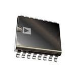
| 封装/外壳 | 16-SOIC(0.295",7.50mm 宽) |
| 封装/箱体 | SOIC-16 |
| 工作温度 | -40°C ~ 85°C |
| 工厂包装数量 | 47 |
| 技术 | 磁耦合 |
| 接收器滞后 | 15mV |
| 数据速率 | 16Mbps |
| 最大工作温度 | + 85 C |
| 最大数据速率 | 16 Mb/s |
| 最小工作温度 | - 40 C |
| 标准包装 | 47 |
| 电压-电源 | 3.3V,5V |
| 电压-隔离 | 2500Vrms |
| 电源电压-最大 | 5.5 V |
| 电源电压-最小 | 2.7 V |
| 电源电流 | 75 mA |
| 类型 | RS422, RS485 |
| 系列 | ADM2485 |
| 绝缘电压 | 2.5 kVrms |
| 脉宽失真(最大) | - |
| 视频文件 | http://www.digikey.cn/classic/video.aspx?PlayerID=1364138032001&width=640&height=505&videoID=2219593469001http://www.digikey.cn/classic/video.aspx?PlayerID=1364138032001&width=640&height=505&videoID=2219593470001http://www.digikey.cn/classic/video.aspx?PlayerID=1364138032001&width=640&height=505&videoID=2219614223001 |
| 设计资源 | |
| 输入-输入侧1/输入侧2 | 2/1 |
| 通道数 | 3 |
| 通道数量 | 1 Channel |
| 通道类型 | 单向 |
| 隔离式电源 | 是 |
| 驱动器/接收器数 | 1/1 |


- 商务部:美国ITC正式对集成电路等产品启动337调查
- 曝三星4nm工艺存在良率问题 高通将骁龙8 Gen1或转产台积电
- 太阳诱电将投资9.5亿元在常州建新厂生产MLCC 预计2023年完工
- 英特尔发布欧洲新工厂建设计划 深化IDM 2.0 战略
- 台积电先进制程称霸业界 有大客户加持明年业绩稳了
- 达到5530亿美元!SIA预计今年全球半导体销售额将创下新高
- 英特尔拟将自动驾驶子公司Mobileye上市 估值或超500亿美元
- 三星加码芯片和SET,合并消费电子和移动部门,撤换高东真等 CEO
- 三星电子宣布重大人事变动 还合并消费电子和移动部门
- 海关总署:前11个月进口集成电路产品价值2.52万亿元 增长14.8%


PDF Datasheet 数据手册内容提取
High Speed, Isolated RS-485 Transceiver with Integrated Transformer Driver ADM2485 FEATURES FUNCTIONAL BLOCK DIAGRAM Half-duplex, isolated RS-485 transceiver VDD1 D1 D2 VDD2 Integrated oscillator driver for external transformer PROFIBUS® compliant OSC ADM2485 Complies with ANSI/TIA/EIA RS-485-A-98 and N ISO 8482:1987(E) RTS O DE OUT TI Data rate: 16 Mbps LA O 5 V or 3.3 V operation (VDD1) TxD C IS 50 nodes on bus NI A V High common-mode transient immunity: >25 kV/μs AL A G Isolated DE OUT status output RxD B Thermal shutdown protection RE Safety and regulatory approvals VUDL Er eCceorgtinfiictiaotne: o 2f5 C0o0n Vfo rrmmsi tfyo r 1 minute per UL 1577 GND1 GND2 06021-001 Figure 1. DIN V VDE V 0884-10 (VDE V 0884-10):2006-12 Reinforced insulation, V = 560 V peak IORM Operating temperature range: –40°C to +85°C Wide-body, 16-lead SOIC package APPLICATIONS Isolated RS-485/RS-422 interfaces PROFIBUS networks Industrial field networks Multipoint data transmission systems GENERAL DESCRIPTION The ADM2485 differential bus transceiver is an integrated, The ADM2485 driver has an active high enable. The driver galvanically isolated component designed for bidirectional data differential outputs and the receiver differential inputs are communication on multipoint bus transmission lines. It is connected internally to form a differential input/output port designed for balanced transmission lines and complies with that imposes minimal loading on the bus when the driver is ANSI/TIA/EIA RS-485-A-98 and ISO 8482:1987(E). disabled or when V or V = 0 V. Also provided is an active DD1 DD2 high receiver disable that causes the receive output to enter a The device employs Analog Devices, Inc., iCoupler® technology high impedance state. to combine a 3-channel isolator, a three-state differential line driver, and a differential input receiver into a single package. An The device has current-limiting and thermal shutdown features on-chip oscillator outputs a pair of square waveforms that drive to protect against output short circuits and situations where bus an external transformer to provide isolated power with an external contention might cause excessive power dissipation. The part is transformer. The logic side of the device can be powered with fully specified over the industrial temperature range and is available either a 5 V or a 3.3 V supply, and the bus side is powered with in a 16-lead, wide-body SOIC package. an isolated 5 V supply. Rev. A Information furnished by Analog Devices is believed to be accurate and reliable. However, no responsibility is assumed by Analog Devices for its use, nor for any infringements of patents or other One Technology Way, P.O. Box 9106, Norwood, MA 02062-9106, U.S.A. rights of third parties that may result from its use. Specifications subject to change without notice. No license is granted by implication or otherwise under any patent or patent rights of Analog Devices. Tel: 781.329.4700 www.analog.com Trademarks and registered trademarks are the property of their respective owners. Fax: 781.461.3113 ©2007 Analog Devices, Inc. All rights reserved.
ADM2485 TABLE OF CONTENTS Features..............................................................................................1 Typical Performance Characteristics...........................................10 Applications.......................................................................................1 Test Circuits.....................................................................................13 Functional Block Diagram..............................................................1 Circuit Description.........................................................................14 General Description.........................................................................1 Electrical Isolation......................................................................14 Revision History...............................................................................2 Truth Tables.................................................................................14 Specifications.....................................................................................3 Thermal Shutdown....................................................................14 Timing Specifications..................................................................5 Receiver Fail-Safe Inputs...........................................................14 Package Characteristics...............................................................6 Magnetic Field Immunity..........................................................15 Regulatory Information...............................................................6 Applications Information..............................................................16 Insulation and Safety-Related Specifications............................6 PCB Layout.................................................................................16 VDE 0884-2 Insulation Characteristics.....................................7 Transformer Suppliers...............................................................16 Absolute Maximum Ratings............................................................8 Applications Diagram................................................................16 ESD Caution..................................................................................8 Outline Dimensions.......................................................................17 Pin Configuration and Function Descriptions.............................9 Ordering Guide..........................................................................17 REVISION HISTORY 12/07—Rev. 0 to Rev. A Updated Format..................................................................Universal Changes to Features Section............................................................1 Changes to Table 4............................................................................6 Changes to VDE 0884-2 Insulation Characteristics Section......7 Changes to PCB Section and Figure 34.......................................16 Updated Outline Dimensions.......................................................17 1/07—Revision 0: Initial Version Rev. A | Page 2 of 20
ADM2485 SPECIFICATIONS 2.7 V ≤ V ≤ 5.5 V, 4.75 V ≤ V ≤ 5.25 V, T = T to T , unless otherwise noted. DD1 DD2 A MIN MAX Table 1. Parameter Min Typ Max Unit Test Conditions/Comments DRIVER Differential Outputs Differential Output Voltage, V 5 V R = ∞, see Figure 21 OD 2.1 5 V R = 50 Ω (RS-422), see Figure 21 2.1 5 V R = 27 Ω (RS-485), see Figure 21 2.1 5 V V = –7 V to +12 V, V ≥ 4.75 V, see Figure 22 TST DD1 Δ|V | for Complementary Output States 0.2 V R = 27 Ω or 50 Ω, see Figure 21 OD Common-Mode Output Voltage, V 3 V R = 27 Ω or 50 Ω, see Figure 21 OC Δ|V | for Complementary Output States 0.2 V R = 27 Ω or 50 Ω, see Figure 21 OC Output Short-Circuit Current, V = High 60 200 mA −7 V ≤ V ≤ +12 V OUT OUT Output Short-Circuit Current, V = Low 60 200 mA −7 V ≤ V ≤ +12 V OUT OUT Bus Enable Output Output High Voltage V − 0.1 V I = 20 μA DD2 ODE V − 0.3 V − 0.1 V I = 1.6 mA DD2 DD2 ODE V − 0.4 V − 0.2 V I = 4 mA DD2 DD2 ODE Output Low Voltage 0.1 V I = −20 μA ODE 0.1 0.3 V I = −1.6 mA ODE 0.2 0.4 V I = −4 mA ODE Logic Inputs Input High Voltage 0.7 V V TxD, RTS, RE DD1 Input Low Voltage 0.25 V V TxD, RTS, RE DD1 CMOS Logic Input Current (TxD, RTS, RE) −10 +0.01 +10 μA TxD, RTS, RE = V or 0 V DD1 RECEIVER Differential Inputs Differential Input Threshold Voltage, V −200 +200 mV −7 V ≤ V ≤ +12V TH CM Input Hysteresis 70 mV −7 V ≤ V ≤ +12V CM Input Resistance (A, B) 20 30 kΩ −7 V ≤ V ≤ +12V CM Input Current (A, B) 0.6 mA V = +12 V IN −0.35 mA V = −7 V IN RxD Logic Output Output High Voltage V − 0.1 V I = +20 μA, V − V = +0.2 V DD1 OUT A B V − 0.4 V − 0.2 V I = +1.5 mA, V − V = +0.2 V DD1 DD1 OUT A B Output Low Voltage 0.1 V I = −20 μA, V − V = −0.2 V OUT A B 0.2 0.4 V I = −4 mA, V − V = −0.2 V OUT A B Output Short-Circuit Current 7 85 mA V = GND or V OUT CC Tristate Output Leakage Current ±1 μA 0.4 V ≤ V ≤ 2.4 V OUT TRANSFORMER DRIVER Oscillator Frequency 400 500 600 kHz V = 5.5 V DD1 230 330 430 kHz V = 3.3 V DD1 Switch-On Resistance 0.5 1.5 Ω Start-Up Voltage 2.2 2.5 V Rev. A | Page 3 of 20
ADM2485 Parameter Min Typ Max Unit Test Conditions/Comments POWER SUPPLY CURRENT Logic Side 2.5 mA RTS = 0 V, V = 5.5 V DD1 2.3 mA 2.5 Mbps, V = 5.5 V, see Figure 23 DD1 5.0 6.5 mA 16 Mbps, V = 5.5 V, see Figure 23 DD1 1.26 mA RTS = 0 V, V = 3.3 V DD1 1.5 mA 2.5 Mbps, V = 3.3 V, see Figure 23 DD1 2.9 mA 16 Mbps, V = 3.3 V, see Figure 23 DD1 Bus Side 1.7 2.5 mA RTS = 0 V 49.0 mA 2.5 Mbps, RTS = V , see Figure 23 for DD1 load conditions 55.0 75.0 mA 16 Mbps, RTS = V , see Figure 23 for DD1 load conditions COMMON-MODE TRANSIENT IMMUNITY1 25 kV/μs Transient magnitude = 800 V, V = 1 kV CM HIGH FREQUENCY COMMON-MODE 100 mV V = +5 V, −2 V < V < +7 V, HF TEST2 NOISE IMMUNITY 1 MHz < f < 50 MHz, see Figure 24 TEST 1 CM is the maximum common-mode voltage slew rate that can be sustained while maintaining specification-compliant operation. VCM is the common-mode potential difference between the logic and bus sides. The transient magnitude is the range over which the common mode is slewed. The common-mode voltage slew rates apply to both rising and falling common-mode voltage edges. Rev. A | Page 4 of 20
ADM2485 TIMING SPECIFICATIONS 2.7 V ≤ V ≤ 5.5 V, 4.75 V ≤ V ≤ 5.25 V, T = T to T , unless otherwise noted. DD1 DD2 A MIN MAX Table 2. Parameter Min Typ Max Unit Test Conditions/Comments DRIVER Maximum Data Rate 16 Mbps Propagation Delay Input-to-Output t , t 25 45 55 ns R = 54 Ω, C = C = 100 pF, see Figure 25 PLH PHL LDIFF L1 L2 RTS-to-DE OUT Propagation Delay 20 35 55 ns See Figure 26 Driver Output-to-Output, tSKEW 2 5 ns RLDIFF = 54 Ω, CL1 = CL2 = 100 pF, see Figure 2 and Figure 25 Rise/Fall Time, t, t 5 15 ns R = 54 Ω, C = C = 100 pF, see Figure 2 and Figure 25 R F LDIFF L1 L2 Enable Time 43 53 ns See Figure 4 and Figure 27 Disable Time 43 55 ns See Figure 4 and Figure 27 Enable Skew, |t − t |, |t − t | 1 3 ns See Figure 4 and Figure 27 AZH BZL AZL BZH Disable Skew, |t − t |, |t − t | 2 5 ns See Figure 4 and Figure 27 AHZ BLZ ALZ BHZ RECEIVER Propagation Delay, t , t 25 45 55 ns C = 15 pF, see Figure 3 and Figure 28 PLH PHL L Differential Skew, t 5 ns C = 15 pF, see Figure 3 and Figure 28 SKEW L Enable Time 3 13 ns R = 1 kΩ, C = 15 pF, see Figure 5 and Figure 29 L L Disable Time 3 13 ns R = 1 kΩ, C = 15 pF, see Figure 5 and Figure 29 L L Timing Diagrams 3V 1.5V 1.5V 0V 0.7VDD1 tPLH tPHL B RTS 0.5VDD1 0.5VDD1 VOUT 1/2VOUT tZL tLZ 0.3VDD1 A tSKEW = |tPLH – tPHL| 2.3V +VOUT 90% POINT 90% POINT A – B VOH + 0.5V VOL 0V 10% POINT 10% POINT tZH tHZ VOH –VOUT tR tF 06021-012 A – B 2.3V VOH – 0.5V 0V 06021-014 Figure 2. Driver Propagation Delay, Rise/Fall Timing Figure 4. Driver Enable/Disable Timing 0.7VDD1 RE 0.5VDD1 0.5VDD1 0.3VDD1 A – B 0V 0V tZL tLZ 1.5V tPLH tPHL RxD OUTPUT LOW VOH + 0.5V VOL VOH tZH tHZ OUTPUT HIGH RxD 1.5V tSKEW= |tPLH – tPHL| 1.5V VOL 06021-013 Rx0DV 1.5V VOH – 0.5V VOH 06021-015 Figure 3. Receiver Propagation Delay Figure 5. Receiver Enable/Disable Timing Rev. A | Page 5 of 20
ADM2485 PACKAGE CHARACTERISTICS Table 3. Parameter Symbol Min Typ Max Unit Test Conditions Resistance (Input-to-Output)1 R 1012 Ω I-O Capacitance (Input-to-Output)1 C 3 pF f = 1 MHz I-O Input Capacitance2 C 4 pF I Input IC Junction-to-Case Thermal Resistance θ 33 °C/W Thermocouple located at center of JCI package underside Output IC Junction-to-Case Thermal Resistance θ 28 °C/W Thermocouple located at center of JCO package underside 1 Device considered a 2-terminal device: Pin 1 to Pin 8 are shorted together and Pin 9 to Pin 16 are shorted together. 2 Input capacitance is from any input data pin to ground. REGULATORY INFORMATION Table 4. ADM2485 Approvals Organization Approval Type Notes UL Recognized under the Component Recognition In accordance with UL 1577, each ADM2485 is proof tested by Program of Underwriters Laboratories, Inc. applying an insulation test voltage ≥3000 V rms for 1 second (current leakage detection limit = 5 μA). VDE Certified according to DIN V VDE V 0884-10 In accordance with DIN V VDE V 0884-10, each ADM2485 is proof (VDE V 0884-10): 2006-12 tested by applying an insulation test voltage ≥1050 V peak for 1 second (partial discharge detection limit = 5 pC). INSULATION AND SAFETY-RELATED SPECIFICATIONS Table 5. Parameter Symbol Value Unit Conditions Rated Dielectric Insulation Voltage 2500 V rms 1-minute duration Minimum External Air Gap (External Clearance) L(I01) 5.15 min mm Measured from input terminals to output terminals, shortest distance through air Minimum External Tracking (Creepage) L(I02) 5.5 min mm Measured from input terminals to output terminals, shortest distance along body Minimum Internal Gap (Internal Clearance) 0.017 min mm Insulation distance through insulation Tracking Resistance (Comparative Tracking Index) CTI >175 V DIN IEC 112/VDE 0303-1 Isolation Group IIIa Material Group (DIN VDE 0110: 1989-01, Table 1) Rev. A | Page 6 of 20
ADM2485 VDE 0884-2 INSULATION CHARACTERISTICS This isolator is suitable for basic electrical isolation only within the safety limit data. Maintenance of the safety data must be ensured by means of protective circuits. An asterisk (*) on packages denotes DIN V VDE V 0884-10 approval. Table 6. Description Symbol Characteristic Unit Installation Classification per DIN VDE 0110 for Rated Mains Voltage ≤150 V rms I to IV ≤300 V rms I to III ≤400 V rms I to II Climatic Classification 40/85/21 Pollution Degree (DIN VDE 0110: 1989-01, Table 1) 2 Maximum Working Insulation Voltage V 560 V peak IORM Input-to-Output Test Voltage V PR Method B1: V × 1.875 = V , 100% Production Tested, t = 1 sec, Partial Discharge < 5 pC 1050 V peak IORM PR m Method A (After Environmental Tests, Subgroup 1): V × 1.6 = V , t = 60 sec, IORM PR m Partial Discharge <5 pC 896 V peak Method A (After Input and/or Safety Test, Subgroup 2/3): V × 1.2 = V , t = 60 sec, IORM PR m Partial Discharge <5 pC 672 V peak Highest Allowable Overvoltage1 V 4000 V peak TR Safety-Limiting Values2 Case Temperature T 150 °C S Input Current I 265 mA S, INPUT Output Current I 335 mA S, OUTPUT Insulation Resistance at T 3 R >109 Ω S S 1 Transient overvoltage, tTR = 10 sec. 2 The safety-limiting value is the maximum value allowed in the event of a failure. See Figure 14 for the thermal derating curve. 3 VIO = 500 V. Rev. A | Page 7 of 20
ADM2485 ABSOLUTE MAXIMUM RATINGS T = 25°C, unless otherwise noted. All voltages are relative to Stresses above those listed under Absolute Maximum Ratings A their respective grounds. may cause permanent damage to the device. This is a stress rating only; functional operation of the device at these or any Table 7. other conditions above those indicated in the operational Parameter Rating section of this specification is not implied. Exposure to absolute VDD1 −0.5 V to +6 V maximum rating conditions for extended periods may affect VDD2 −0.5 V to +6 V device reliability. Digital Input Voltage (RTS, RE, TxD) −0.5 V to V + 0.5 V DD1 Digital Output Voltage RxD −0.5 V to V + 0.5 V ESD CAUTION DD1 DE OUT −0.5 V to V + 0.5 V DD2 D1, D2 13 V Driver Output/Receiver Input Voltage −9 V to +14 V Operating Temperature Range −40°C to +85°C Storage Temperature Range −55°C to +150°C Average Output Current per Pin −35 mA to +35 mA θ Thermal Impedance 73°C/W JA Lead Temperature Soldering (10 sec) 300°C Vapor Phase (60 sec) 215°C Infrared (15 sec) 220°C Rev. A | Page 8 of 20
ADM2485 PIN CONFIGURATION AND FUNCTION DESCRIPTIONS D1 1 16 VDD2 D2 2 15 GND2 GND1 3 ADM2485 14 GND2 VDD1 4 TOP VIEW 13 B RxD 5 (Not to Scale) 12 A RE 6 11 GND2 RTTxDS 78 190 DGEN DO2UT 06021-002 Figure 6. Pin Configuration Table 8. Pin Function Description Pin No. Mnemonic Function 1 D1 Transformer Driver Terminal 1. 2 D2 Transformer Driver Terminal 2. 3 GND Ground, Logic Side. 1 4 V Power Supply, Logic Side (3.3 V or 5 V). Decoupling capacitor to GND required; capacitor value should be DD1 1 between 0.01 μF and 0.1 μF. 5 RxD Receiver Output Data. This output is high when (A − B) > 200 mV and low when (A − B) < −200 mV. The output is tristated when the receiver is disabled, that is, when RE is driven high. 6 RE Receiver Enable Input. This is an active-low input. Driving this input low enables the receiver; driving it high disables the receiver. 7 RTS Driver Enable Input. Driving this input high enables the driver; driving it low disables the driver. 8 TxD Driver Input. Data to be transmitted by the driver is applied to this input. 9, 11, 14, 15 GND Ground, Bus Side. 2 10 DE OUT Driver Enable Status Output. 12 A Noninverting Driver Output/Receiver Input. When the driver is disabled or V or V is powered down, DD1 DD2 Pin A is put in a high impedance state to avoid overloading the bus. 13 B Inverting Driver Output/Receiver Input. When the driver is disabled or V or V is powered down, DD1 DD2 Pin B is put in a high impedance state to avoid overloading the bus. 16 V Power Supply, Bus Side (Isolated 5 V Supply). Decoupling capacitor to GND required; capacitor value DD2 2 should be between 0.01 μF and 0.1 μF. Rev. A | Page 9 of 20
ADM2485 TYPICAL PERFORMANCE CHARACTERISTICS 2.40 60 2.35 2.30 IDD1_RE_ENABLE_VDD1 = 5.5V Y (ns) 50 tPLHA tPHLB mA) ELA 40 RRENT ( 22..2250 ATION D 30 tPLHB tPHLA U G C A Y P L 2.15 O PP PR 20 SU 2.10 ER IDD2_DE_ENABLE_VDD1 = 5.5V DRIV 10 2.05 2.00 0 –40 –20 0TEMPER20ATURE (°4C0) 60 80 06021-016 –40 –20 0TEMPER20ATURE (°4C0) 60 80 06021-019 Figure 7. Unloaded Supply Current vs. Temperature Figure 10. Driver Propagation Delay vs. Temperature 5.0 60 4.5 IDD1_PROFIBUS LOAD_TxD = 16Mbps_VDD1 = 5.00V s) Rx PROP DELAY,tPLH_VDD2 = 5.00V n 50 A) 4.0 AY ( m L URRENT ( 33..05 IIDDDD11__NPROO LFOIBAUDS_T LxODA =D 1_6TMxDb p=s 2_MVDbDp1s _=V 5D.0D01V = 5.00V ATION DE 40 Rx PROP DELAY,tPHL_VDD2 = 5.00V C 2.5 G 30 PLY 2.0 OPA P R I SUDD1 11..05 IDD1_NO LOAD_TxD = 2Mbps_VDD1 = 5.00V EIVER P 20 EC 10 0.5 R 0 0 –40 –20 0TEMPER20ATURE (°4C0) 60 80 06021-017 –40 –20 0TEMPER20ATURE (°4C0) 60 80 06021-020 Figure 8. Logic Side Supply Current (IDD1 = 1 mA) vs. Temperature Figure 11. Receiver Propagation Delay vs. Temperature 60 IDD2_ PROFIBUS LOAD_TxD = 16Mbps_VDD2 = 5.00V 50 A) m NT ( 40 IDD2_PROFIBUS LOAD_TxD = 2Mbps_VDD2 = 5.00V DI RE 3 R U C 30 Y L PP B U 20 S D2 ID IDD2_NO LOAD_TxD = 16Mbps_VDD2 = 5.00V 10 A IDD2_NO LOAD_TxD = 2Mbps_VDD2 = 5.00V 2 0 –40 –20 0TEMPER20ATURE (°4C0) 60 80 06021-018 CCHH31 22..00VV ΩΩ CH2 2.0V Ω MIT2 80..00pnss/ p1t.25GS/s A CH3 2.60V 06021-021 Figure 9. Bus Side Supply Current (IDD2 = 2 mA) vs. Temperature Figure 12. Driver/Receiver Propagation Delay, Low to High (RLDIFF = 54 Ω, CL1 = CL2 = 100 pF) Rev. A | Page 10 of 20
ADM2485 60 50 A) 1 NT (m 40 E R R 30 U C T U TP 20 U O 10 3 0 CCHH31 21..00VV ΩΩ CH2 1.0V Ω MT 1 0 . 0 n1s9.8000nAs CH1 120mV 06021-022 0 1 OUTP2UT VOLTAG3E (V) 4 5 06021-025 Figure 13. Driver/Receiver Propagation Delay, High to Low Figure 16. Output Current vs. Receiver Output Low Voltage (RLDIFF = 54 Ω, CL1 = CL2 = 100 pF) 350 4.75 4.74 300 A) m 4.73 G CURRENT ( 225000 SIDE 2 VOLTAGE (V) 44..7721 MITIN 150 SIDE 1 TPUT 4.70 LI U TY- 100 O 4.69 E F A S 50 4.68 00 50CASE TEMP1E0R0ATURE (°C)150 200 06021-023 4.67–40 –20 0TEMPER20ATURE (°4C0) 60 80 06021-031 Figure 14. Thermal Derating Curve, Dependence of Safety-Limiting Values Figure 17. Receiver Output High Voltage vs. Temperature (IDD2 = –4 mA) with Case Temperature per VDE 0884-2 0 0.32 –10 0.30 OUTPUT CURRENT (mA) ––––23450000 OUTPUT VOLTAGE (V) 000...222864 0.22 –60 –70 0.20 0 1 OUTP2UT VOLTAG3E (V) 4 5 06021-024 –40 –20 0TEMPER20ATURE (°4C0) 60 80 06021-032 Figure 15. Output Current vs. Receiver Output High Voltage Figure 18. Receiver Output Low Voltage vs. Temperature (IDD2 = –4 mA) Rev. A | Page 11 of 20
ADM2485 D1 D1 D2 1 1 D2 2 CH1 2.0V Ω CH2 2.0V Ω M8.400n0sn/pst 125MS/s A CH2 1.52V 06021-033 CH1 2.0V Ω CH2 2.0V Ω M1.860nnss/p 6t25MS/s A CH2 1.52V 06021-034 Figure 19. Switching Waveforms Figure 20. Switching Waveforms (50 Ω Pull-Up to VDD1 on D1 and D2) (Break-Before-Make, 50 Ω Pull-Up to VDD1 on D1 and D2) Rev. A | Page 12 of 20
ADM2485 TEST CIRCUITS R A CL1 VOD RLDIFF R VOC 06021-003 B CL2 06021-007 Figure 21. Driver Voltage Measurement Figure 25. Driver Propagation Delay 375Ω DE OUT VOD3 60Ω VTEST RTS N 150Ω O 50pF Figure 22. Driver Voltage3 7M5Ωeasurement 06021-004 TxD NIC ISOLATI A LV A A RxD G B DE OUT RE RTS ATION 150Ω VDD1FigurGe N2D61. RTS to DE OUVTD DP2ropGaNgDa2tion Delay 06021-008 L O TxD C IS VDD2 ANI A 195Ω VCC V RxD GAL B 110Ω TxD A S1 110Ω S2 RE 195Ω B 50pF VOUT VDD1 GND1 VDD2 GND2 GND2 06021-005 RTS 06021-009 Figure 23. Supply-Current Measurement Test Circuit Figure 27. Driver Enable/Disable A RTS DE OUT VOUT ATION B RE CL 06021-010 TxD SOL VDD2 Figure 28. Receiver Propagation Delay VCM (HF)RxD ALVANIC I BA 111905ΩΩ 4705n0FΩ FTVEHSFT, +1.5V VCC 2.2kΩ G 110nF S1 GND2 RVEDD1 100nFGND1 VDD2 100nF GND2GND1295Ω 50VΩTES2T22kΩ 06021-006 –1.5VRE IN RE CL VORULT S2 06021-011 Figure 24. High Frequency, Common-Mode Noise Test Circuit Figure 29. Receiver Enable/Disable Rev. A | Page 13 of 20
ADM2485 CIRCUIT DESCRIPTION ELECTRICAL ISOLATION Table 10. Transmitting In the ADM2485, electrical isolation is implemented on the Supply Status Inputs Outputs logic side of the interface. Therefore, the part has two main V V RTS TxD A B DE OUT DD1 DD2 sections: a digital isolation section and a transceiver section On On H H H L H (see Figure 30). Driver input and data enable, applied to the On On H L L H H TxD and RTS pins, respectively, and referenced to logic ground On On L X Z Z L (GND1), are coupled across an isolation barrier to appear at the On Off X X Z Z L transceiver section referenced to isolated ground (GND2). Off On X X Z Z L Similarly, the receiver output, referenced to isolated ground in Off Off X X Z Z L the transceiver section, is coupled across the isolation barrier to appear at the RxD pin referenced to logic ground. Table 11. Receiving iCoupler Technology Supply Status Input Outputs The digital signals are transmitted across the isolation barrier VDD1 VDD2 A − B RE RxD using iCoupler technology. This technique uses chip-scale On On >+0.2 V L or NC H transformer windings to couple the digital signals magnetically On On <–0.2 V L or NC L from one side of the barrier to the other. Digital inputs are On On −0.2 V < A − B < +0.2 V L or NC I encoded into waveforms that are capable of exciting the On On Inputs open L or NC H primary transformer winding. At the secondary winding, the On On X H Z induced waveforms are then decoded into the binary value that On Off X L or NC H was originally transmitted. Off On X L or NC H VDD1 D1 D2 VDD2 Off Off X L or NC L ISOLATION OSC BARRIER THERMAL SHUTDOWN A TxD ENCODE DECODE D The ADM2485 contains thermal shutdown circuitry that B protects the part from excessive power dissipation during fault RTS ENCODE DECODE DE OUT conditions. Shorting the driver outputs to a low impedance source can result in high driver currents. The thermal sensing circuitry detects the increase in die temperature under this RxD DECODE ENCODE R condition and disables the driver outputs. This circuitry is RE DIGITAL ISOLATION TRANSCEIVER designed to disable the driver outputs when a die temperature GND1 GND2 06021-026 oatf a1 5t0em°Cp iesr raetaucrhee odf. A14s 0t°hCe .d evice cools, the drivers are re-enabled Figure 30. ADM2485 Digital Isolation and Transceiver Sections RECEIVER FAIL-SAFE INPUTS TRUTH TABLES The receiver input includes a fail-safe feature that guarantees a Table 10 and Table 11 use the abbreviations found in Table 9. Logic high RxD output when the A and B inputs are floating or open-circuited. Table 9. Truth Table Abbreviations Letter Description H High level I Indeterminate L Low level X Irrelevant Z High impedance (off) NC Disconnected Rev. A | Page 14 of 20
ADM2485 MAGNETIC FIELD IMMUNITY For example, at a magnetic field frequency of 1 MHz, the maximum allowable magnetic field of 0.2 kGauss induces a Because iCouplers use a coreless technology, no magnetic voltage of 0.25 V at the receiving coil, which is about 50% of the components are present and the problem of magnetic saturation sensing threshold and does not cause a faulty output transition. of the core material does not exist. Therefore, iCouplers have Similarly, if such an event occurs during a transmitted pulse and essentially infinite dc field immunity. The following analysis it is the worst-case polarity, it reduces the received pulse from defines the conditions under which this can occur. The ADM2485 >1.0 V to 0.75 V, still well above the 0.5 V sensing threshold of 3.3 V operating condition is examined because it represents the the decoder. most susceptible mode of operation. Figure 32 shows the magnetic flux density values in terms of The limitation on the iCoupler ac magnetic field immunity is more familiar quantities, such as maximum allowable current set by the condition in which the induced error voltage in the flow at given distances from the ADM2485 transformers. receiving coil (the bottom coil, in this case) is made sufficiently large, either to falsely set or reset the decoder. The voltage 1000 induced across the bottom coil is given by A) DISTANCE = 1m k V=⎜⎛−dβ⎟⎞∑πr2; n = 1, 2 … N (1) NT ( 100 ⎝ dt ⎠ n RE UR DISTANCE = 5mm where, if the pulses at the transformer output are greater than C 10 E L 1.0 V in amplitude: B A W DISTANCE = 100mm β is the magnetic flux density (gauss). O 0 L N is the number of turns in the receiving coil. AL M rn is the radius of nth turn in the receiving coil (cm). XIMU 0.1 The decoder has a sensing threshold of about 0.5 V; therefore, A M there is a 0.5 V margin where induced voltages can be tolerated. Greiqvueinr etmhee nget othmaet ttrhye o ifn tdhuec reedc eviovlitnagg ec oisi,l aatn md oasnt ,i m50p%o soefd t he 0.011k 10kMAGNETI1C0 F0kIELD FREQ1MUENCY (Hz1)0M 100M 06021-028 Figure 32. Maximum Allowable Current for 0.5 V margin at the decoder, a maximum allowable magnetic Various Current-to-ADM2485 Spacings field is calculated, as shown in Figure 31. At combinations of strong magnetic field and high frequency, 100 any loops formed by printed circuit board (PCB) traces could induce sufficiently large error voltages to trigger the thresholds TIC 10 of succeeding circuitry. Care must be taken in the layout of such E E MAGNGAUSS) 1 t races to avoid this possibility. Lk ALLOWABDENSITY ( 0.1 MUM FLUX XI 0.01 A M 0.0011k 10kMAGNETIC10 F0kIELD FREQ1MUENCY (Hz1)0M 100M 06021-027 Figure 31. Maximum Allowable External Magnetic Flux Density vs. Magnetic Field Frequency Rev. A | Page 15 of 20
ADM2485 APPLICATIONS INFORMATION PCB LAYOUT APPLICATIONS DIAGRAM The ADM2485 isolated RS-485 transceiver requires no external The ADM2485 integrates a transformer driver that, when used interface circuitry for the logic interfaces. Power supply bypassing with an external transformer and LDO, generates an isolated is required at the input and output supply pins (see Figure 33). 5 V power supply, to be supplied between V and GND. DD2 2 Bypass capacitors are most conveniently connected between D1 and D2 of the ADM2485 drive the center-tapped Pin 3 and Pin 4 for VDD1 and between Pin 15 and Pin 16 for Transformer T1. A pair of Schottky diodes and a smoothing VDD2. The capacitor value must be between 0.01 μF and 0.1 μF. capacitor is used to create a rectified signal from the secondary The total lead length between both ends of the capacitor and winding. The ADP3330 linear voltage regulator provides a the input power supply pin must not exceed 20 mm. regulated 5 V power supply to the ADM2485 bus-side circuitry Bypassing between Pin 9 and Pin 16 is also recommended (VDD2), as shown in Figure 34. unless the ground wires on the VDD2 side are connected close to When the ADM2485 is powered by 3.3 V on the logic side, a the package. 1CT:2.2CT Transformer T1 is required to step up the 3.3 V to D1 VDD2 6 V, ensuring enough headroom for the ADP3330 LDO to D2 GND2 output a regulated 5 V output. GND1 GND2 VDD1 ADM2485 B If ADM2485 is powered by 5 V on the logic side, a 1CT:1.5CT RxD A RE GND2 Transformer T1 is required, ensuring enough headroom for the RTTxDS DGEN DO2UT 06021-029 ADP3330 LDO to output a regulated 5 V output. Figure 33. Recommended Printed Circuit Board Layout ISOLATION BARRIER In applications involving high common-mode transients, care 1N5817 ERR NR 5V IN OUT must be taken to ensure that board coupling across the isolation VCC 22µF ADP3330 10µF barrier is minimized. Furthermore, the board layout must be 10µF SD MLC GND designed such that any coupling that does occur equally affects T11N5817 all pins on a given component side. VCC ISO 5V Failure to ensure this can cause voltage differentials between pins exceeding the device absolute maximum ratings, thereby 100nF 100nF leading to latch-up or permanent damage. VDD1 D1 D2 VDD2 TRANSFORMER SUPPLIERS ADM2485 The transformer primarily used with the ADM2485 must be a GND1 GND2 ctreanntsefro-trampepre dm tursatn bsefo sremt teor pwrionvdiidneg t. hTeh me tinurimnsu rmat iroe qouf itrheed 06021-030 Figure 34. Applications Diagram output voltage at the maximum anticipated load with the minimum input voltage. Table 12 shows ADM2485 transformer suppliers. Table 12. Transformer Suppliers Manufacturer Primary Voltage 3.3 V Primary Voltage 5 V Coilcraft DA2304-AL DA2303-AL C&D Technologies 782485/35C 782485/55C Rev. A | Page 16 of 20
ADM2485 OUTLINE DIMENSIONS 10.50 (0.4134) 10.10 (0.3976) 16 9 7.60 (0.2992) 7.40 (0.2913) 1 10.65 (0.4193) 8 10.00 (0.3937) 1.27 (0.0500) 0.75 (0.0295) BSC 2.65 (0.1043) 0.25 (0.0098) 45° 0.30 (0.0118) 2.35 (0.0925) 8° 0.10 (0.0039) 0° COPLANARITY 0.10 0.51 (0.0201) SPLEAATNIENG 0.33 (0.0130) 1.27 (0.0500) 0.31 (0.0122) 0.20 (0.0079) 0.40 (0.0157) COMPLIANTTO JEDEC STANDARDS MS-013-AA C(RINOEFNPEATRRREOENNLCLTEIHN EOGSN EDLSIYM)AEANNRDSEI AORRNOESU NANORDEET DAIN-PO MPFRIFLO LMPIIMRLELIATIMTEEER TFSEO; RIRN ECUQHSU EDI VIINMA LEDENENSSTIIOGSN NFS.OR 032707-B Figure 35. 16-Lead Standard Small Outline Package [SOIC_W] Wide Body (RW-16) Dimensions shown in millimeters and (inches) ORDERING GUIDE Model Data Rate (Mbps) Temperature Range Package Description Package Option ADM2485BRWZ1 16 −40°C to +85°C 16-Lead SOIC_W RW-16 ADM2485BRWZ-REEL71 16 −40°C to +85°C 16-Lead SOIC_W RW-16 1 Z = RoHS Compliant Part. Rev. A | Page 17 of 20
ADM2485 NOTES Rev. A | Page 18 of 20
ADM2485 NOTES Rev. A | Page 19 of 20
ADM2485 NOTES ©2007 Analog Devices, Inc. All rights reserved. Trademarks and registered trademarks are the property of their respective owners. D06021-0-12/07(A) Rev. A | Page 20 of 20
Mouser Electronics Authorized Distributor Click to View Pricing, Inventory, Delivery & Lifecycle Information: A nalog Devices Inc.: EVAL-ADM2485EB3Z EVAL-ADM2485EB5Z ADM2485BRWZ-REEL7 ADM2485BRWZ