 Datasheet下载
- 型号: ADM2487EBRWZ
- 制造商: Analog
- 库位|库存: xxxx|xxxx
- 要求:
| 数量阶梯 | 香港交货 | 国内含税 |
| +xxxx | $xxxx | ¥xxxx |
查看当月历史价格
查看今年历史价格
ADM2487EBRWZ产品简介:
ICGOO电子元器件商城为您提供ADM2487EBRWZ由Analog设计生产,在icgoo商城现货销售,并且可以通过原厂、代理商等渠道进行代购。 ADM2487EBRWZ价格参考。AnalogADM2487EBRWZ封装/规格:数字隔离器, RS422,RS485 数字隔离器 2500Vrms 3 通道 500kbps 25kV/µs CMTI 16-SOIC(0.295",7.50mm 宽)。您可以下载ADM2487EBRWZ参考资料、Datasheet数据手册功能说明书,资料中有ADM2487EBRWZ 详细功能的应用电路图电压和使用方法及教程。
ADM2487EBRWZ 是 Analog Devices Inc. 生产的一款数字隔离器,广泛应用于需要电气隔离的通信接口场景中。以下是其主要应用场景:

1. 工业自动化与控制:
   - 在工业环境中,设备之间通常需要通过 RS-485 或 CAN 总线进行通信。ADM2487E 提供了必要的隔离功能,防止不同设备之间的地电位差导致的损坏或干扰。它适用于 PLC(可编程逻辑控制器)、DCS(分布式控制系统)和 SCADA(数据采集与监控系统)等。

2. 楼宇自动化:
   - 楼宇自动化系统中的传感器、执行器和控制器之间需要可靠的通信。该芯片可以确保信号传输的稳定性和安全性,避免因长距离布线带来的噪声和干扰问题。

3. 电力系统与能源管理:
   - 电力系统中,变电站、智能电表和其他电力设备之间的通信要求高可靠性。ADM2487E 的隔离特性有助于保护敏感电路免受高压浪涌的影响,同时保证数据的准确传输。

4. 医疗设备:
   - 医疗设备如监护仪、心电图机等需要在患者和设备之间提供安全隔离,以防止电流泄漏对患者造成伤害。这款数字隔离器能够满足医疗行业严格的电气安全标准。

5. 汽车电子:
   - 现代汽车内部有多个电子控制单元(ECU),它们通过车载网络相互通信。ADM2487E 可用于隔离这些网络连接,提高系统的抗噪能力和可靠性,特别是在恶劣的工作环境下。

6. 通信基础设施:
   - 在通信基站、服务器机房等场合,设备间的数据交换频繁且复杂。使用 ADM2487E 进行隔离可以有效减少电磁干扰(EMI),提升系统的整体性能。

总之,ADM2487EBRWZ 凭借其卓越的隔离性能和低功耗设计,在各种需要可靠、安全通信接口的应用领域发挥着重要作用。
| 参数 | 数值 |
| 产品目录 | 集成电路 (IC)半导体 |
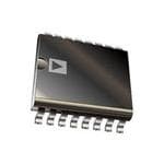
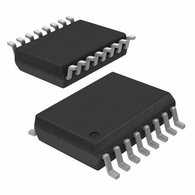
| 描述 | IC TXRX RS485 ISO W/ESD 16SOIC数字隔离器 2.5kV Sgnl Iso Full/Half Duplex |
| 产品分类 | |
| 品牌 | Analog Devices |
| 产品手册 | |
| 产品图片 |
|
| rohs | 符合RoHS无铅 / 符合限制有害物质指令(RoHS)规范要求 |
| 产品系列 | 接口 IC,数字隔离器,Analog Devices ADM2487EBRWZiCoupler® |
| 数据手册 | |
| 产品型号 | ADM2487EBRWZ |
| 产品目录页面 | |
| 产品种类 | |
| 传播延迟时间 | 700 ns |
| 供应商器件封装 | 16-SOIC W |
| 关闭 | No Shutdown |
| 功率耗散 | 152 mW |
| 包装 | 管件 |
| 协议 | RS422,RS485 |
| 双工 | 全 |
| 商标 | Analog Devices |
| 安装类型 | 表面贴装 |
| 安装风格 | SMD/SMT |
| 封装 | Tube |
| 封装/外壳 | 16-SOIC(0.295",7.50mm 宽) |
| 封装/箱体 | SOIC-16 |
| 工作温度 | -40°C ~ 85°C |
| 工厂包装数量 | 47 |
| 接收器滞后 | 15mV |
| 数据速率 | 500kbps |
| 最大工作温度 | + 85 C |
| 最大数据速率 | 500 kb/s |
| 最小工作温度 | - 40 C |
| 标准包装 | 47 |
| 电压-电源 | 3V,5V |
| 电源电压-最大 | 5.5 V |
| 电源电压-最小 | 3 V |
| 电源电流 | 4 mA |
| 类型 | RS-485 |
| 系列 | ADM2487E |
| 绝缘电压 | 2.5 kVrms |
| 通道数量 | 3 Channel |
| 驱动器/接收器数 | 1/1 |


- 商务部:美国ITC正式对集成电路等产品启动337调查
- 曝三星4nm工艺存在良率问题 高通将骁龙8 Gen1或转产台积电
- 太阳诱电将投资9.5亿元在常州建新厂生产MLCC 预计2023年完工
- 英特尔发布欧洲新工厂建设计划 深化IDM 2.0 战略
- 台积电先进制程称霸业界 有大客户加持明年业绩稳了
- 达到5530亿美元!SIA预计今年全球半导体销售额将创下新高
- 英特尔拟将自动驾驶子公司Mobileye上市 估值或超500亿美元
- 三星加码芯片和SET,合并消费电子和移动部门,撤换高东真等 CEO
- 三星电子宣布重大人事变动 还合并消费电子和移动部门
- 海关总署:前11个月进口集成电路产品价值2.52万亿元 增长14.8%

PDF Datasheet 数据手册内容提取
2.5 kV Isolated RS-485 Transceivers with Integrated Transformer Driver ADM2482E/ADM2487E FEATURES FUNCTIONAL BLOCK DIAGRAM Isolated RS-485/RS-422 transceivers, configurable as half VDD1 D1 D2 VDD2 duplex or full duplex OSC Integrated oscillator driver for external transformer DE ±15 kV ESD protection on RS-485 input/output pins N O Complies with TIA/EIA-485-A-98 and ISO 8482:1987(E) TI A Y L Data rate: 500 kbps/16 Mbps TxD O 5 V or 3.3 V operation (VDD1) NIC IS Z 256 nodes on bus VA True fail-safe receiver inputs RxD GAL A Safety and regulatory approvals B RE UL recognition: 2500 V rms for 1 minute per UL 1577 VDDEI cNe VrtVifDicEa Vte 0s 8o8f 4c-o1n0f o(VrmDEit Vy 0884-10):2006-12 GND1 GND2 07379-001 Figure 1. V = 560 V peak IORM Thermal shutdown protection Operating temperature range: −40°C to +85°C Wide-body, 16-lead SOIC package APPLICATIONS Isolated RS-485/RS-422 interfaces Industrial field networks Multipoint data transmission systems GENERAL DESCRIPTION The ADM2482E/ADM2487E are isolated data transceivers with power. The logic side of the device is powered with either a 5 V ±15 kV ESD protection and are suitable for high speed, half- or a 3.3 V supply, and the bus side is powered with an isolated duplex or full-duplex communication on multipoint transmission 3.3 V supply. lines. For half-duplex operation, the transmitter outputs and The ADM2482E/ADM2487E driver has an active high enable, receiver inputs share the same transmission line. Transmitter and the receiver has an active low enable. The driver output Output Pin Y is linked externally to Receiver Input Pin A, and enters a high impedance state when the driver enable signal Transmitter Output Pin Z to Receiver Input Pin B. The parts are is low. The receiver output enters a high impedance state when designed for balanced transmission lines and comply with the receiver enable signal is high. TIA/EIA-485-A-98 and ISO 8482:1987(E). The device has current-limiting and thermal shutdown features The devices employ the Analog Devices, Inc., iCoupler® to protect against output short circuits and situations where bus technology to combine a 3-channel isolator, a three-state contention might cause excessive power dissipation. The part is differential line driver, and a differential input receiver into a fully specified over the industrial temperature range of −40°C to single package. An on-chip oscillator outputs a pair of square +85°C and is available in a 16-lead, wide-body SOIC package. waveforms that drive an external transformer to provide isolated Rev. A Information furnished by Analog Devices is believed to be accurate and reliable. However, no responsibility is assumed by Analog Devices for its use, nor for any infringements of patents or other One Technology Way, P.O. Box 9106, Norwood, MA 02062-9106, U.S.A. rights of third parties that may result from its use. Specifications subject to change without notice. No license is granted by implication or otherwise under any patent or patent rights of Analog Devices. Tel: 781.329.4700 www.analog.com Trademarks and registered trademarks are the property of their respective owners. Fax: 781.461.3113 ©2008–2009 Analog Devices, Inc. All rights reserved.
ADM2482E/ADM2487E TABLE OF CONTENTS Features .............................................................................................. 1 Test Circuits ..................................................................................... 12 Applications ....................................................................................... 1 Switching Characteristics .............................................................. 13 Functional Block Diagram .............................................................. 1 Circuit Description......................................................................... 14 General Description ......................................................................... 1 Electrical Isolation ...................................................................... 14 Revision History ............................................................................... 2 Truth Tables................................................................................. 14 Specifications ..................................................................................... 3 Thermal Shutdown .................................................................... 15 Timing Specifications .................................................................. 4 True Fail-Safe Receiver Inputs .................................................. 15 Package Characteristics ............................................................... 5 Magnetic Field Immunity .......................................................... 15 Regulatory Information ............................................................... 5 Applications Information .............................................................. 16 Insulation and Safety-Related Specifications ............................ 5 Printed Circuit Board Layout ................................................... 16 VDE 0884-2 Insulation Characteristics ..................................... 6 Transformer Suppliers ............................................................... 16 Absolute Maximum Ratings ............................................................ 7 Isolated Power Supply Circuit .................................................. 16 ESD Caution .................................................................................. 7 Typical Applications ................................................................... 17 Pin Configuration and Function Descriptions ............................. 8 Outline Dimensions ....................................................................... 18 Typical Performance Characteristics ............................................. 9 Ordering Guide .......................................................................... 18 REVISION HISTORY 2/09—Rev. 0 to Rev. A Edits to Features ................................................................................ 1 Added Table 5 .................................................................................... 5 Changes to Table 6 ............................................................................ 5 Added Table 7 .................................................................................... 6 Changes to Figure 9 ........................................................................ 13 Added Table 13 ............................................................................... 16 Changes to Ordering Guide .......................................................... 18 5/08—Revision 0: Initial Version Rev. A | Page 2 of 20
ADM2482E/ADM2487E SPECIFICATIONS Each voltage is relative to its respective ground; 3.0 V ≤ V ≤ 5.5 V, 3.0 V ≤ V ≤ 3.6 V. All minimum/maximum specifications apply DD1 DD2 over the entire recommended operation range, unless otherwise noted. All typical specifications are at T = 25°C, V = 5 V, V = 3.3 V, A DD1 DD2 unless otherwise noted. Table 1. Parameter Symbol Min Typ Max Unit Test Conditions SUPPLY CURRENT Power Supply Current, Logic Side I DD1 TxD/RxD Data Rate < 500 kbps 3.5 mA Unloaded output ADM2487E TxD/RxD Data Rate = 500 kbps 4 mA Half-duplex configuration, R = 120 Ω, see Figure 25 TERMINATION ADM2482E TxD/RxD Data Rate = 16 Mbps 6.0 mA Half-duplex configuration, R = 120 Ω, see Figure 25 TERMINATION Power Supply Current, Bus Side I DD2 TxD/RxD Data Rate < 500 kbps 17 mA Unloaded output ADM2487E TxD/RxD Data Rate = 500 kbps 40 mA V = 3.6 V, half-duplex DD2 configuration, R = 120 Ω, TERMINATION see Figure 25 ADM2482E TxD/RxD Data Rate = 16 Mbps 50 mA V = 3.6 V, half-duplex DD2 configuration, R = 120 Ω, TERMINATION see Figure 25 DRIVER Differential Outputs Differential Output Voltage, Loaded |VOD2| 2.0 5.0 V RL = 100 Ω (RS-422), see Figure 19 1.5 5.0 V R = 54 Ω (RS-485), see Figure 19 L |VOD3| 1.5 5.0 V −7 V ≤ VTEST ≤ +12 V, see Figure 20 ∆|VOD| for Complementary Output States ∆|VOD| 0.2 V RL = 54 Ω or 100 Ω, see Figure 19 Common-Mode Output Voltage VOC 3.0 V RL = 54 Ω or 100 Ω, see Figure 19 ∆|VOC| for Complementary Output States ∆|VOC| 0.2 V RL = 54 Ω or 100 Ω, see Figure 19 Short-Circuit Output Current I 250 mA OS Output Leakage Current (Y, Z) I 125 μA DE = 0 V, RE = 0 V, V = 0 V or O CC 3.6 V, V = 12 V IN −100 μA DE = 0 V, RE = 0 V, V = 0 V or CC 3.6 V, V = −7 V IN Logic Inputs Input Threshold Low V 0.25 × V V DE, RE, TxD IL DD1 Input Threshold High V 0.7 × V V DE, RE, TxD IH DD1 Input Current I −10 +0.01 +10 μA DE, RE, TxD I RECEIVER Differential Inputs Differential Input Threshold Voltage V −200 −125 −30 mV −7 V < V < +12 V TH CM Input Voltage Hysteresis V 15 mV V = 0 V HYS OC Input Current (A, B) I 125 μA DE = 0 V, V = 0 V or 3.6 V, I DD V = 12 V IN −125 μA DE = 0 V, V = 0 V or 3.6 V, DD V = −7 V IN Line Input Resistance R 96 kΩ −7 V < V < +12 V IN CM Logic Outputs Output Voltage Low V 0.2 0.4 V I = 1.5 mA, V − V = −0.2 V OLRxD ORxD A B Output Voltage High V V − 0.3 V − 0.2 V I = −1.5 mA, V − V = 0.2 V OHRxD DD1 DD1 ORxD A B Short-Circuit Current I 100 mA OS Tristate Output Leakage Current I ±1 μA V = 5.0 V, 0 V < V < V OZR DD1 O DD1 Rev. A | Page 3 of 20
ADM2482E/ADM2487E Parameter Symbol Min Typ Max Unit Test Conditions TRANSFORMER DRIVER Oscillator Frequency f 400 500 600 kHz V = 5.0 V OSC DD1 230 330 430 kHz V = 3.3 V DD1 Switch-On Resistance R 0.5 1.5 Ω ON Start-Up Voltage V 2.2 2.5 V START COMMON-MODE TRANSIENT IMMUNITY1 25 kV/μs V = 1 kV, transient CM magnitude = 800 V 1 CM is the maximum common-mode voltage slew rate that can be sustained while maintaining specification-compliant operation. VCM is the common-mode potential difference between the logic and bus sides. The transient magnitude is the range over which the common-mode is slewed. The common-mode voltage slew rates apply to both rising and falling common-mode voltage edges. TIMING SPECIFICATIONS T = −40°C to +85°C, unless otherwise noted. A Table 2. ADM2482E Parameter Symbol Min Typ Max Unit Test Conditions DRIVER Propagation Delay t , t 100 ns R = 54 Ω, C = 100 pF, see Figure 21 and Figure 26 DPLH DPHL DIFF L Output Skew t 8 ns R = 54 Ω, C = 100 pF, see Figure 21 and Figure 26 DSKEW DIFF L Rise Time/Fall Time t , t 15 ns R = 54 Ω, C = 100 pF, see Figure 21 and Figure 26 DR DF DIFF L Enable Time t , t 120 ns R = 110 Ω, C = 50 pF, see Figure 22 and Figure 28 ZL ZH L L Disable Time t , t 150 ns R = 110 Ω, C = 50 pF, see Figure 22 and Figure 28 LZ HZ L L RECEIVER Propagation Delay t , t 110 ns C = 15 pF, see Figure 23 and Figure 27 PLH PHL L Output Skew t 8 ns C = 15 pF, see Figure 23 and Figure 27 SKEW L Enable Time t , t 13 ns R = 1 kΩ, C = 15 pF, see Figure 24 and Figure 29 ZL ZH L L Disable Time t , t 13 ns R = 1 kΩ, C = 15 pF, see Figure 24 and Figure 29 LZ HZ L L Table 3. ADM2487E Parameter Symbol Min Typ Max Unit Test Conditions DRIVER Propagation Delay t , t 250 700 ns R = 54 Ω, C = 100 pF, see Figure 21 and Figure 26 DPLH DPHL DIFF L Output Skew t 100 ns R = 54 Ω, C = 100 pF, see Figure 21 and Figure 26 DSKEW DIFF L Rise Time/Fall Time t , t 200 1100 ns R = 54 Ω, C = 100 pF, see Figure 21 and Figure 26 DR DF DIFF L Enable Time t , t 2.5 μs R = 110 Ω, C = 50 pF, see Figure 22 and Figure 28 ZL ZH L L Disable Time t , t 200 ns R = 110 Ω, C = 50 pF, see Figure 22 and Figure 28 LZ HZ L L RECEIVER Propagation Delay t , t 200 ns C = 15 pF, see Figure 23 and Figure 27 PLH PHL L Output Skew t 30 ns C = 15 pF, see Figure 23 and Figure 27 SKEW L Enable Time t , t 13 ns R = 1 kΩ, C = 15 pF, see Figure 24 and Figure 29 ZL ZH L L Disable Time t , t 13 ns R = 1 kΩ, C = 15 pF, see Figure 24 and Figure 29 LZ HZ L L Rev. A | Page 4 of 20
ADM2482E/ADM2487E PACKAGE CHARACTERISTICS Table 4. Parameter Symbol Min Typ Max Unit Test Conditions Resistance (Input-to-Output)1 R 1012 Ω I-O Capacitance (Input-to-Output)1 C 3 pF f = 1 MHz I-O Input Capacitance2 C 4 pF I Input IC Junction-to-Case Thermal Resistance θ 33 °C/W Thermocouple located at center of JCI package underside Output IC Junction-to-Case Thermal Resistance θ 28 °C/W Thermocouple located at center of JCO package underside 1 Device considered a 2-terminal device: Pin 1 to Pin 8 are shorted together, and Pin 9 to Pin 16 are shorted together. 2 Input capacitance is from any input data pin to ground. REGULATORY INFORMATION Table 5. ADM2482E/ADM2487E Approvals Organization Approval Type Notes UL Recognized under the component recognition In accordance with UL 1577, each ADM2482E/ADM2487E is proof program of underwriters laboratories, Inc. tested by applying an insulation test voltage ≥3000 V rms for 1 second (current leakage detection limit = 5 μA) VDE Certified according to DIN V VDE V 0884-10 In accordance with DIN V VDE V 0884-10, each ADM2482E/ADM2487E (VDE V 0884-10):2006-12 is proof tested by applying an insulation test voltage ≥1050 V peak for 1 second (partial discharge detection limit = 5 pC) INSULATION AND SAFETY-RELATED SPECIFICATIONS Table 6. Parameter Symbol Value Unit Conditions Rated Dielectric Insulation Voltage 2500 V rms 1-minute duration Minimum External Air Gap (External Clearance) L(I01) 5.15 min mm Measured from input terminals to output terminals, shortest distance through air Minimum External Tracking (Creepage) L(I02) 5.5 min mm Measured from input terminals to output terminals, shortest distance along body Minimum Internal Gap (Internal Clearance) 0.017 min mm Insulation distance through insulation Tracking Resistance (Comparative Tracking Index) CTI >175 V DIN IEC 112/VDE 0303-1 Isolation Group IIIa Material group (DIN VDE 0110: 1989-01, Table 1) Rev. A | Page 5 of 20
ADM2482E/ADM2487E VDE 0884-2 INSULATION CHARACTERISTICS This isolator is suitable for basic electrical isolation only within the safety limit data. Maintenance of the safety data must be ensured by means of protective circuits. An asterisk (*) on packages denotes DIN V VDE V 0884-10 approval. Table 7. Description Conditions Symbol Characteristic Unit CLASSIFICATIONS Installation Classification per DIN VDE 0110 for Rated Mains Voltage ≤150 V rms I to IV ≤300 V rms I to III ≤400 V rms I to II Climatic Classification 40/85/21 Pollution Degree (DIN VDE 0110: 1989-01, see Table 1) 2 VOLTAGE Maximum Working Insulation Voltage V 560 V peak IORM Input-to-Output Test Voltage V PR V × 1.875 = V , 100% production tested, t = IORM PR m Method b1 1 sec, partial discharge < 5 pC 1050 V peak Method a: 896 V peak After Environmental Tests, Subgroup 1 V × 1.6 = V , t = 60 sec, partial discharge <5 pC IORM PR m Method a 672 V peak After Input and/or Safety Test, V × 1.2 = V , t = 60 sec, partial discharge <5 pC IORM PR m Subgroup 2/3): Highest Allowable Overvoltage1 V 4000 V peak TR SAFETY-LIMITING VALUES2 Case Temperature T 150 °C S Input Current I 265 mA S, INPUT Output Current I 335 mA S, OUTPUT Insulation Resistance at T 3 R >109 Ω S S 1 Transient overvoltage, tTR = 10 sec. 2 The safety-limiting value is the maximum value allowed in the event of a failure. See Figure 3 for the thermal derating curve. 3 VIO = 500 V. Rev. A | Page 6 of 20
ADM2482E/ADM2487E ABSOLUTE MAXIMUM RATINGS Each voltage is relative to its respective ground; T = 25°C, A Stresses above those listed under Absolute Maximum Ratings unless otherwise noted. may cause permanent damage to the device. This is a stress rating only; functional operation of the device at these or any Table 8. other conditions above those indicated in the operational Parameter Rating section of this specification is not implied. Exposure to absolute V −0.5 V to +6 V DD1 maximum rating conditions for extended periods may affect V −0.5 V to +6 V DD2 device reliability. Digital Input Voltages (DE, RE, TxD) −0.5 V to V + 0.5 V DD1 Digital Output Voltages RxD −0.5 V to VDD1 + 0.5 V ESD CAUTION D1, D2 13 V Driver Output/Receiver Input Voltage Range −9 V to +14 V Average Output Current per Pin −35 mA to +35 mA ESD (Human Body Model) on A, B, Y, and ±15 kV Z pins Operating Temperature Range −40°C to +85°C Storage Temperature Range −55°C to +150°C Lead Temperature Soldering (10 sec) 300°C Vapor Phase (60 sec) 215°C Infrared (15 sec) 220°C Rev. A | Page 7 of 20
ADM2482E/ADM2487E PIN CONFIGURATION AND FUNCTION DESCRIPTIONS D1 1 16 VDD2 D2 2 15 GND2 GND1 3 ADM2482E/ 14 A ADM2487E VDD1 4 13 B TOP VIEW RxD 5 (Not to Scale) 12 Z RE 6 11 Y DE 7 10 NC TxD 8NC = NO CONNECT9 GND2 07379-002 Figure 2. Pin Configuration Table 9. Pin Function Descriptions Pin No. Mnemonic Description 1 D1 Transformer Driver Terminal 1. 2 D2 Transformer Driver Terminal 2. 3 GND Ground, Logic Side. 1 4 V Power Supply, Logic Side (3.3 V or 5 V). Decoupling capacitor to GND required; capacitor value should be DD1 1 between 0.01 μF and 0.1 μF. 5 RxD Receiver Output Data. This output is high when (A – B) > +200 mV and low when (A – B) < –200 mV. The output is tristated when the receiver is disabled, that is, when RE is driven high. 6 RE Receiver Enable Input. This is an active low input. Driving this input low enables the receiver; driving it high disables the receiver. 7 DE Driver Enable Input. Driving this input high enables the driver; driving it low disables the driver. 8 TxD Transmit Data. 9 GND Ground, Bus Side. 2 10 NC No Connect. This pin must be left floating. 11 Y Driver Noninverting Output. 12 Z Driver Inverting Output. 13 B Receiver Inverting Input. 14 A Receiver Noninverting Input. 15 GND Ground, Bus Side. 2 16 V Power Supply, Bus Side (Isolated 3.3 V Supply). Decoupling capacitor to GND required; capacitor value should be DD2 2 between 0.01 μF and 0.1 μF. Rev. A | Page 8 of 20
ADM2482E/ADM2487E TYPICAL PERFORMANCE CHARACTERISTICS 2.30 60 NO LOAD NO LOAD 54Ω LOAD 54Ω LOAD 2.25 120Ω LOAD 50 120Ω LOAD A) A) m 2.20 m (D1 (D140 D D T I 2.15 T I N N RE RE 30 R R U 2.10 U C C LY LY 20 PP 2.05 PP U U S S 10 2.00 1.95–40 –15 TE1M0PERATURE3 (5°C) 60 8507379-029 0–40 –15 TE1M0PERATURE3 (5°C) 60 8507379-032 Figure 3. ADM2487E IDD1 Supply Current vs. Temperature Figure 6. ADM2482E Supply Current vs. Temperature (See Figure 25) (Data Rate = 500 kbps, VDD1 = 5 V, VDD2 = 3.3 V, DE = 1 V, RE = 0 V) (Data Rate = 16 Mbps, VDD1 = 5 V, VDD2 = 3.3 V, DE = 1, RE = 0 V) 40 600 t 35 DPLH mA) 30 N5142O0Ω ΩL L OLOAOADADD AY (ns) 500 tDPHL T I (DD225 ON DEL 400 LY CURREN 2105 PROPAGATI 320000 SUPP 10 DRIVER 100 5 0–40 –15 TE1M0PERATURE3 (5°C) 60 8507379-030 0–40 –20 0TEMPER2A0TURE (°4C0) 60 80 07379-033 Figure 4. ADM2487E IDD2 Supply Current vs. Temperature (See Figure 25) Figure 7. ADM2487E Driver Propagation Delay vs. Temperature (Data Rate = 500 kbps, VDD1 = 5 V, VDD2 = 3.3 V, DE = 1 V, RE = 0 V) 4.0 70 NO LOAD 3.9 54Ω LOAD 65 (mA)D133..87 120Ω LOAD DELAY (ns) 6505 tDPtLDHPHL PPLY CURRENT ID333...654 R PROPAGATION 54430505 U E S 3.3 RIV 30 D 3.2 25 3.1–40 –15 TE1M0PERATURE3 5(°C) 60 8507379-031 20–40 –15 TE1M0PERATURE3 (5°C) 60 8507379-034 Figure 5. ADM2482E IDD1 Supply Current vs. Temperature (Data Rate = Figure 8. ADM2482E Driver Propagation Delay vs. Temperature 16 Mbps, VDD1 = 5 V, VDD2 = 3.3 V, DE = 1 V, RE = 0 V) Rev. A | Page 9 of 20
ADM2482E/ADM2487E 0 0.32 –10 0.30 RRENT (mA) ––2300 OLTAGE (V) 00..2286 T CU –40 UT V U P TP UT 0.24 U –50 O O 0.22 –60 –70 0.20 0 1 OUTP2UT VOLTAG3E (V) 4 5 07379-016 –40 –20 0TEMPER20ATURE (°4C0) 60 80 07379-019 Figure 9. Output Current vs. Receiver Output High Voltage Figure 12. Receiver Output Low Voltage vs. Temperature (IDD2 = 4 mA) 60 50 D1 A) T (m 40 N E R UR 30 1 C T U TP 20 U O 10 D2 2 0 0 1 OUTP2UT VOLTAG3E (V) 4 5 07379-017 CH1 2.0V Ω CH2 2.0V Ω M8.400n0sn/pst 125MS/s A CH2 1.52V 07379-020 Figure 10. Output Current vs. Receiver Output Low Voltage Figure 13. Switching Waveforms (50 Ω Pull-Up to VDD1 on D1 and D2) 4.75 4.74 D1 4.73 V) GE ( 4.72 TA D2 OL 4.71 1 V T U P 4.70 T U O 4.69 4.68 4.67 –40 –20 0TEMPER20ATURE (°4C0) 60 80 07379-018 CH1 2.0V Ω CH2 2.0V Ω M1.860nnss/p 6t25MS/s A CH2 1.52V 07379-021 Figure 11. Receiver Output High Voltage vs. Temperature Figure 14. Switching Waveforms (IDD2 = −4 mA) (Break-Before-Make, 50 Ω Pull-Up to VDD1 on D1 and D2) Rev. A | Page 10 of 20
ADM2482E/ADM2487E T TxD 1 TxD Z, B 1 Z, B 2 Y, A 2 Y, A RxD 4 RxD 4 CCHH13 22..0000VV CCHH24 22..0000VV MT 2 0 0 n4s7.80% A CH2 1.72V07379-035 CCHH13 22..00VV ΩΩ CCHH24 22..00VV ΩΩ AM 4C0H.02n s 11..2658GVS/s IT16.0ps/pt07379-037 Figure 15. ADM2487E Driver/Receiver Propagation Delay, Low to High Figure 17. ADM2482E Driver/Receiver Propagation Delay, High to Low (RDIFF = 54 Ω, CL1 = CL2 = 100 pF) (RDIFF = 54 Ω, CL1 = CL2 = 100 pF) T TxD 1 TxD Z, B 1 Z, B 2 Y, A 2 Y, A RxD 4 RxD 4 CCHH13 22..0000VV CCHH24 22..0000VV MT 2 0 0 n4s8.60% A CH2 1.72V07379-036 CCHH13 22..00VV ΩΩ CCHH24 22..00VV ΩΩ AM 4C0H.02n s 11..2658GVS/s IT16.0ps/pt07379-038 Figure 16. ADM2487E Driver/Receiver Propagation Delay, High to Low Figure 18. ADM2482E Driver/Receiver Propagation Delay, Low to High (RDIFF = 54 Ω, CL1 = CL2 = 100 pF) (RDIFF = 54 Ω, CL1 = CL2 = 100 pF) Rev. A | Page 11 of 20
ADM2482E/ADM2487E TEST CIRCUITS Y RL 2 TxD VOD2 VOUT VCC Z R2L Y RL VOC 110Ω TxD S1 S2 07379-003 DE Z 5C0LpF 07379-007 Figure 19. Driver Voltage Measurement Figure 22. Driver Enable/Disable Y 375Ω A TxD VOD3 60Ω Z 375Ω VTEST 07379-004 B RE CL VOUT 07379-008 Figure 20. Driver Voltage Measurement Figure 23. Receiver Propagation Delay +1.5V VCC S1 Y CL –1.5V RL S2 TxD RDIFF RE CL VOUT Z CL 07379-006 RE IN 07379-009 Figure 21. Driver Propagation Delay Figure 24. Receiver Enable/Disable VDD2 VDD1 VDD2 DE N O TI LA Y O TxD C IS Z 120Ω NI A V AL A G RxD B RE GND1 GND2 07379-005 Figure 25. Supply Current Measurement Test Circuit Rev. A | Page 12 of 20
ADM2482E/ADM2487E SWITCHING CHARACTERISTICS VDD1 VDD1/2 VDD1/2 0V VDD1 tDPLH tDPHL DE 0.5VDD1 0.5VDD1 Z 1/2VO 0V VO tZL 2.3V tLZ Y tDSKEW = |tDPLH –tDPHL| Y, Z VOL+ 0.5V V+DVIFOF 90% POINT VDIFF= V(Y)– V(Z) 90% POINT tZH 2.3V tHZ VVOOLH –VO 10% POINT tDR tDF 10% POINT 07379-010 Y, Z VOH– 0.5V 0V 07379-012 Figure 26. Driver Propagation Delay, Rise/Fall Timing Figure 28. Driver Enable/Disable Timing 0.7VDD1 RE 0.5VDD1 0.5VDD1 0.3VDD1 A–B 0V 0V tZL tLZ 1.5V tPLH tPHL RxD OUTPUTLOW VOL+ 0.5V VOL VOH tZH tHZ OUTPUTHIGH RxD 1.5V tSKEW= |tPLH–tPHL| 1.5V VOL 07379-011 R0xVD 1.5V VOH– 0.5V VOH 07379-013 Figure 27. Receiver Propagation Delay Figure 29. Receiver Enable/Disable Timing Rev. A | Page 13 of 20
ADM2482E/ADM2487E CIRCUIT DESCRIPTION ELECTRICAL ISOLATION TRUTH TABLES In the ADM2482E/ADM2487E, electrical isolation is imple- The truth tables in this section use the abbreviations found in mented on the logic side of the interface. Therefore, the part Table 10. has two main sections: a digital isolation section and a transceiver Table 10. Truth Table Abbreviations section (see Figure 30). Driver input and data enable applied to Letter Description the TxD and DE pins, respectively, and referenced to logic ground (GND) are coupled across an isolation barrier to appear at the H High level 1 transceiver section referenced to isolated ground (GND). Simi- I Indeterminate 2 larly, the receiver output, referenced to isolated ground in the L Low level transceiver section, is coupled across the isolation barrier to X Irrelevant appear at the RxD pin referenced to logic ground. Z High impedance (off) NC Disconnected iCoupler Technology The digital signals transmit across the isolation barrier using Table 11. Transmitting iCoupler technology. This technique uses chip scale transformer Supply Status Inputs Outputs windings to couple the digital signals magnetically from one VDD1 V DD2 DE TxD Y Z side of the barrier to the other. Digital inputs are encoded into On On H H H L waveforms that are capable of exciting the primary transformer On On H L L H winding. At the secondary winding, the induced waveforms are On On L X Z Z decoded into the binary value that was originally transmitted. On Off X X Z Z Off On L X Z Z Positive and negative logic transitions at the input cause narrow Off Off X X Z Z pulses (~1 ns) to be sent to the decoder, via the transformer. The decoder is bistable and is, therefore, either set or reset by Table 12. Receiving the pulses, indicating input logic transitions. In the absence of Supply Status Inputs Outputs logic transitions at the input for more than ~1 μs, a periodic set V V A − B RE RxD of refresh pulses indicative of the correct input state are sent to DD1 DD2 On On >−0.03 V L or NC H ensure dc correctness at the output. If the decoder receives no On On <−0.2 V L or NC L internal pulses for more than about 5 μs, then the input side is On On −0.2 V < A − B < −0.03 V L or NC I assumed to be unpowered or nonfunctional, in which case the On On Inputs open L or NC H output is forced to a default state (see Table 10). On On X H Z VDD1 D1 D2 VDD2 On Off X L or NC H Off Off X L or NC L OSC ISOLATION BARRIER DE ENCODE DECODE Y TxD ENCODE DECODE D Z A RxD ENCODE DECODE R B RE DIGITAL ISOLATION TRANSCEIVER GND1 GND2 07379-022 Figure 30. ADM2482E/ADM2487E Digital Isolation and Transceiver Sections Rev. A | Page 14 of 20
ADM2482E/ADM2487E THERMAL SHUTDOWN Given the geometry of the receiving coil and an imposed requirement that the induced voltage is, at most, 50% of the The ADM2482E/ADM2487E contain thermal shutdown 0.5 V margin at the decoder, a maximum allowable magnetic circuitry that protects the parts from excessive power dissipa- field can be determined using Figure 31. tion during fault conditions. Shorting the driver outputs to a 100 low impedance source can result in high driver currents. The thermal sensing circuitry detects the increase in die temperature C under this condition and disables the driver outputs. This TI 10 E cteirmcupietrrayt uisr ed eosfi 1g5n0e°dC t ois dreisaacbhleed t. hAes dthriev dere voiucetp cuotosl sw, thheen d ar idvieer s MAGNAUSS) E G 1 are re-enabled at a temperature of 140°C. ABLY (k TRUE FAIL-SAFE RECEIVER INPUTS ALLOWDENSIT 0.1 Tthhaet trhecee rievceeri ivnepr uotus thpauvt ei sa htirguhe wfahile-nsa tfhe ef eiantpuurtes t ahraet oepnesunr oers MUM FLUX XI 0.01 A shorted. During line idle conditions, when no driver on the M bus is enabled, the voltage across a terminating resistance at trhecee rievceeri ivnepr uint pthurte dshecoaldyss tsop e0c Vif.i eWd ibthet twraedenit i−o2n0a0l tmraVns acneidv ers, 0.0011k 10kMAGNETI1C0 F0kIELD FREQ1MUENCY (Hz1)0M 100M07379-023 +200 mV mean that external bias resistors are required on the Figure 31. Maximum Allowable External Magnetic Flux Density A and B pins to ensure that the receiver outputs are in a known For example, at a magnetic field frequency of 1 MHz, the state. The true fail-safe receiver input feature eliminates the maximum allowable magnetic field of 0.2 kgauss induces a need for bias resistors by specifying the receiver input threshold voltage of 0.25 V at the receiving coil. This is about 50% of the between −30 mV and −200 mV. The guaranteed negative thre- sensing threshold and does not cause a faulty output transition. shold means that when the voltage between A and B decays to Similarly, if such an event occurs during a transmitted pulse and 0 V, the receiver output is guaranteed to be high. is the worst-case polarity, it reduces the received pulse from MAGNETIC FIELD IMMUNITY >1.0 V to 0.75 V, still well above the 0.5 V sensing threshold of the decoder. The limitation on the magnetic field immunity of the iCoupler is set by the condition in which an induced voltage in the Figure 32 shows the magnetic flux density values in terms of receiving coil of the transformer is large enough to either more familiar quantities, such as maximum allowable current falsely set or reset the decoder. The following analysis defines flow at given distances away from the ADM2482E/ADM2487E the conditions under which this may occur. The 3 V operating transformers. condition of the ADM2482E/ADM2487E is examined because 1000 it represents the most susceptible mode of operation. A) DISTANCE = 1m The pulses at the transformer output have an amplitude greater T (k 100 N than 1 V. The decoder has a sensing threshold of about 0.5 V, E RR DISTANCE = 5mm thus establishing a 0.5 V margin in which induced voltages can U C 10 be tolerated. LE B A The voltage induced across the receiving coil is given by W DISTANCE = 100mm O 1 L L V =⎜⎝⎛−ddtβ⎟⎠⎞∑πrn2;n=1,2,K,N XIMUM A 0.1 A where: M βN iiss tthhee mnuagmnbeetric o ffl utuxr dnesn isni ttyh (eg raeucsesi)v.i ng coil. 0.011k 10kMAGNETIC10 F0kIELD FREQ1MUENCY (Hz1)0M 100M 07379-024 rn is the radius of the nth turn in the receiving coil (cm). Figure 32. Maximum Allowable Current for Various Current-to-ADM2482E/ADM2487E Spacings With combinations of strong magnetic field and high frequency, any loops formed by PCB traces can induce error voltages large enough to trigger the thresholds of succeeding circuitry. Care should be taken in the layout of such traces to avoid this possibility. Rev. A | Page 15 of 20
ADM2482E/ADM2487E APPLICATIONS INFORMATION PRINTED CIRCUIT BOARD LAYOUT ISOLATED POWER SUPPLY CIRCUIT The isolated RS-485 transceiver of the ADM2482E/ADM2487E The ADM2482E/ADM2487E integrate a transformer driver requires no external interface circuitry for the logic interfaces. that, when used with an external transformer and linear voltage Power supply bypassing is required at the input and output supply regulator (LDO), generates an isolated 3.3 V power supply to be pins (see Figure 33). supplied between V and GND, as shown in Figure 34. DD2 2 Bypass capacitors are most conveniently connected between Pin D1 and Pin D2 of the ADM2482E/ADM2487E drive a Pin 3 and Pin 4 for V and between Pin 15 and Pin 16 for center-tapped Transformer T1. A pair of Schottky diodes and a DD1 V . The capacitor value must be between 0.01 μF and 0.1 μF. smoothing capacitor are used to create a rectified signal from the DD2 The total lead length between both ends of the capacitor and secondary winding. The ADP3330 LDO provides a regulated the input power supply pin must not exceed 20 mm. 3.3 V power supply to the ADM2482E/ADM2487E bus side circuitry (V ). Bypassing Pin 9 and Pin 16 is also recommended unless the DD2 ground pair on each package side is connected close to the When the ADM2482E/ADM2487E are powered by 3.3 V on the package. logic side, a step-up transformer is required to compensate for the forward voltage drop of the Schottky diodes and the voltage D1 VDD2 drop across the regulator. The transformer turns ratio should be D2 ADM2482E GND2 GND1 OR A chosen to ensure just enough headroom for the ADP3330 LDO VDD1 ADM2487E B to output a regulated 3.3 V output under all operating conditions. RxD Z RE TOP VIEW Y If the ADM2482E/ADM2487E are powered by 5 V on the logic (Not to Scale) TDxDE NC = NO CONNECT NGCND2 07379-025 sejuifdfsitec ,ei etnhnoecunyg, aht h shetee tpard-adnrooswfoomnrm tfroearrn ttshufoern rAms DreaPrt i3soh3 os3hu0o lLduD lbdOe b u etso ec dohu.o Ftspeounr t ot aop rteeinmgsuuulmraete d Figure 33. Recommended Printed Circuit Board Layout 3.3 V output under all operating conditions. In applications involving high common-mode transients, care ISOLATION must be taken to ensure that board coupling across the isolation BARRIER 1N5817 ADP3330 barrier is minimized. Furthermore, the board layout must be 3.3V IN OUT designed such that any coupling that does occur equally affects VCC 22µF SD 10µF all pins on a given component side. 10µF ERR Failure to ensure this can cause voltage differentials between MLC T1 1N5817 NRGND pins exceeding the absolute maximum ratings of the device, VCC thereby leading to latch-up or permanent damage. ISOLATED 3.3V 100nF VDD1 D1 D2 VDD2 TRANSFORMER SUPPLIERS ADM2482E/ 100nF The transformer primarily used with the ADM2482E/ADM2487E ADM2487E mof utshte b ter aan csefonrtmere-tra mppuesdt btrea snest ftoor pmreorv iwdein tdhien mg.i nTihmeu tmur nresq ruaitrieod GND1 GND2 07379-026 Figure 34. Applications Diagram output voltage at the maximum anticipated load with the mini- mum input voltage. Table 13 shows ADM2482E/ADM2487E transformer suppliers. Table 13. Transformer Supplies Manufacturer Primary Voltage 3.3 V Primary Voltage 5 V Coilcraft DA2303-AL GA3157 Murata 782482/33VC 782482/53VC Rev. A | Page 16 of 20
ADM2482E/ADM2487E TYPICAL APPLICATIONS line must be terminated at the receiving end in its characteristic impedance, and stub lengths off the main line must be kept as Figure 35 and Figure 36 show typical applications of the short as possible. For a half-duplex operation, this means that ADM2482E/ADM2487E in half-duplex and full-duplex both ends of the line must be terminated, because either end can RS-485 network configurations. Up to 256 transceivers can be the receiving end. be connected to the RS-485 bus. To minimize reflections, the MAXIMUM NUMBER OF TRANSCEIVERS ON BUS = 256 ADM2482E/ ADM2482E/ ADM2487E ADM2487E A A RxD R B B R RxD RE RE RT RT DE DE Z Z TxD D Y Y D TxD A B Z Y A B Z Y R R ADM2482E/ D ADM2482E/ D ADM2487E ADM2487E RxD RE DE TxD RxD RE DE TxD N12..O RISTTOE ISLSA ETQIOUNA LNOTOT STHHOE WCHNA.RACTERISTIC IMPEDANCE OF THE CABLE. 07379-027 Figure 35. ADM2482E/ADM2487E Typical Half-Duplex RS-485 Network MAXIMUM NUMBER OF NODES = 256 MASTER SLAVE A Y RxD R RT D TxD B Z RE DE DE Z B RE TxD D Y RT A R RxD ADM2482E/ ADM2482E/ ADM2487E ADM2487E A B Z Y A B Z Y SLAVE SLAVE R R D D ADM2482E/ ADM2482E/ ADM2487E ADM2487E RxD RE DE TxD RxD RE DE TxD N1.O RTTE ISS EQUALTO THE CHARACTERISTIC IMPEDANCE OF THE CABLE. 07379-028 Figure 36. ADM2482E/ADM2487E Typical Full-Duplex RS-485 Network Rev. A | Page 17 of 20
ADM2482E/ADM2487E OUTLINE DIMENSIONS 10.50 (0.4134) 10.10 (0.3976) 16 9 7.60 (0.2992) 7.40 (0.2913) 1 10.65 (0.4193) 8 10.00 (0.3937) 1.27 (0.0500) 0.75 (0.0295) BSC 2.65 (0.1043) 0.25 (0.0098) 45° 0.30 (0.0118) 2.35 (0.0925) 8° 0.10 (0.0039) 0° COPLANARITY 0.10 0.51 (0.0201) SPLEAATNIENG 0.33 (0.0130) 1.27 (0.0500) 0.31 (0.0122) 0.20 (0.0079) 0.40 (0.0157) COMPLIANTTO JEDEC STANDARDS MS-013-AA C(RINOEFNPEATRRREOENNLCLTEIHN EOGSN EDLSIYM)AEANNRDSEI AORRNOESU NANORDEET DAIN-PO MPFRIFLO LMPIIMRLELIATIMTEEER TFSEO; RIRN ECUQHSU EDI VIINMA LEDENENSSTIIOGSN NFS.OR 032707-B Figure 37. 16-Lead Standard Small Outline Package [SOIC_W] Wide Body (RW-16) Dimensions shown in millimeters and (inches) ORDERING GUIDE Model Data Rate (Mbps) Temperature Range Package Description Package Option ADM2482EBRWZ1 16 −40°C to +85°C 16-Lead SOIC_W RW-16 ADM2482EBRWZ-REEL71 16 −40°C to +85°C 16-Lead SOIC_W RW-16 ADM2487EBRWZ1 0.5 −40°C to +85°C 16-Lead SOIC_W RW-16 ADM2487EBRWZ-REEL71 0.5 −40°C to +85°C 16-Lead SOIC_W RW-16 EVAL-ADM2482EEB3Z Evaluation Board, 3.3 V Supply EVAL2482EEB5Z Evaluation Board, 5 V Supply EVAL-ADM2487EEB3Z Evaluation Board, 3.3 V Supply EVAL2487EEB5Z Evaluation Board, 5 V Supply 1 Z = RoHS Compliant Part. Rev. A | Page 18 of 20
ADM2482E/ADM2487E NOTES Rev. A | Page 19 of 20
ADM2482E/ADM2487E NOTES ©2008–2009 Analog Devices, Inc. All rights reserved. Trademarks and registered trademarks are the property of their respective owners. D07379-0-2/09(A) Rev. A | Page 20 of 20
Mouser Electronics Authorized Distributor Click to View Pricing, Inventory, Delivery & Lifecycle Information: A nalog Devices Inc.: EVAL-ADM2482EEB3Z EVAL-ADM2482EEB5Z EVAL-ADM2487EEB5Z ADM2482EBRWZ-REEL7 EVAL- ADM2487EEB3Z ADM2487EBRWZ-REEL7 ADM2487EBRWZ ADM2482EBRWZ