ICGOO在线商城 > 射频/IF 和 RFID > RF 放大器 > ADL5201ACPZ-R7
 Datasheet下载
- 型号: ADL5201ACPZ-R7
- 制造商: Analog
- 库位|库存: xxxx|xxxx
- 要求:
| 数量阶梯 | 香港交货 | 国内含税 |
| +xxxx | $xxxx | ¥xxxx |
查看当月历史价格
查看今年历史价格
ADL5201ACPZ-R7产品简介:
ICGOO电子元器件商城为您提供ADL5201ACPZ-R7由Analog设计生产,在icgoo商城现货销售,并且可以通过原厂、代理商等渠道进行代购。 ADL5201ACPZ-R7价格参考¥82.54-¥99.05。AnalogADL5201ACPZ-R7封装/规格:RF 放大器, 射频放大器 IC 700MHz 24-LFCSP-WQ(4x4)。您可以下载ADL5201ACPZ-R7参考资料、Datasheet数据手册功能说明书,资料中有ADL5201ACPZ-R7 详细功能的应用电路图电压和使用方法及教程。
ADL5201ACPZ-R7 是由 Analog Devices Inc.(亚德诺半导体公司)生产的一款 RF(射频)放大器,属于低噪声放大器(LNA,Low Noise Amplifier)类别。其主要应用场景包括:

1. 无线通信系统
   ADL5201ACPZ-R7 适用于各种无线通信设备,例如蜂窝基站、中继器和小型蜂窝网络。它能够以低噪声和高增益特性增强接收信号的质量,确保通信的稳定性和可靠性。

2. 雷达与传感器系统
   在雷达和传感器应用中,该放大器可用于提升弱信号的强度,同时保持较低的噪声水平。这在天气雷达、汽车雷达以及工业传感领域尤为重要。

3. 测试与测量设备
   由于其出色的线性度和宽频率范围(支持高达 1 GHz 的频率),ADL5201ACPZ-R7 广泛应用于信号分析仪、频谱分析仪和其他高性能测试设备中,用于精确测量射频信号。

4. 卫星通信与广播
   在卫星地面站或广播系统中,这款放大器可以用来提高接收到的微弱信号的功率,从而改善系统的整体性能。

5. 物联网(IoT)设备
   对于需要长距离传输的 IoT 设备,ADL5201ACPZ-R7 可以帮助增强信号覆盖范围,尤其是在 LoRa 或其他低功耗广域网(LPWAN)技术中。

6. 医疗电子设备
   在某些医疗成像或监测设备中,射频信号处理是关键环节。ADL5201ACPZ-R7 的高精度和低噪声特性使其成为这些应用的理想选择。

总结来说,ADL5201ACPZ-R7 凭借其卓越的低噪声性能、高增益和宽带操作能力,在需要高质量射频信号放大的各种场景中表现出色。
| 参数 | 数值 |
| 产品目录 | |
| 描述 | IC AMP DGTL VGA LN 24LFCSP |
| 产品分类 | |
| 品牌 | Analog Devices Inc |
| 数据手册 | |
| 产品图片 |
|
| 产品型号 | ADL5201ACPZ-R7 |
| PCN组件/产地 | |
| PCN设计/规格 | |
| RF类型 | 通用 |
| rohs | 无铅 / 符合限制有害物质指令(RoHS)规范要求 |
| 产品系列 | - |
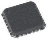
| 供应商器件封装 | 24-LFCSP-WQ(4x4) |
| 其它名称 | ADL5201ACPZ-R7TR |
| 功能 | 数控 VGA |
| 包装 | 带卷 (TR) |
| 封装/外壳 | 24-WFQFN 裸露焊盘,CSP |
| 标准包装 | 1,500 |
| 视频文件 | http://www.digikey.cn/classic/video.aspx?PlayerID=1364138032001&width=640&height=505&videoID=2245193150001 |
| 辅助属性 | SPI 接口 |
| 配用 | /product-detail/zh/ADL5201-EVALZ/ADL5201-EVALZ-ND/4866712 |
| 频率 | 700MHz |


- 商务部:美国ITC正式对集成电路等产品启动337调查
- 曝三星4nm工艺存在良率问题 高通将骁龙8 Gen1或转产台积电
- 太阳诱电将投资9.5亿元在常州建新厂生产MLCC 预计2023年完工
- 英特尔发布欧洲新工厂建设计划 深化IDM 2.0 战略
- 台积电先进制程称霸业界 有大客户加持明年业绩稳了
- 达到5530亿美元!SIA预计今年全球半导体销售额将创下新高
- 英特尔拟将自动驾驶子公司Mobileye上市 估值或超500亿美元
- 三星加码芯片和SET,合并消费电子和移动部门,撤换高东真等 CEO
- 三星电子宣布重大人事变动 还合并消费电子和移动部门
- 海关总署:前11个月进口集成电路产品价值2.52万亿元 增长14.8%


PDF Datasheet 数据手册内容提取
Wide Dynamic Range, High Speed, Digitally Controlled VGA Data Sheet ADL5201 FEATURES FUNCTIONAL BLOCK DIAGRAM −11.5 dB to +20 dB gain range SPI WITH FA, PARALLEL WITH LATCH, 0.5 dB ± 0.1 dB step size UP/DOWN INTERFACE VPOS GND PWUP 150 Ω differential input and output 7.5 dB noise figure at maximum gain MODE0, OIP3 > 50 dBm at 200 MHz MODE1 LOGIC −3 dB upper frequency bandwidth of 700 MHz Multiple control interface options VIN+ 0dB TO 31.5dB VOUT+ Parallel 6-bit control interface (with latch) 150Ω +20dB 150Ω VIN– VOUT– Serial peripheral interface (SPI) (with fast attack) Gain up/down mode WLoiwde p ionwpuert mdyondaem oipc triaonng e PM ADL5201 09388-001 Figure 1. Power-down control Single 5 V supply operation 24-lead, 4 mm × 4 mm LFCSP package APPLICATIONS Differential ADC drivers High IF sampling receivers High output power IF amplification Instrumentation GENERAL DESCRIPTION The ADL5201 is a digitally controlled, variable gain, wide band- The ADL5201 is powered on by applying the appropriate logic width amplifier that provides precise gain control, high IP3, and level to the PWUP pin. The quiescent current of the ADL5201 low noise figure. The excellent distortion performance and high is typically 80 mA in low power mode. When configured in high signal bandwidth make the ADL5201 an excellent gain control performance mode for more demanding applications, the quiescent device for a variety of receiver applications. The ADL5201 also current is 110 mA. When powered down, the ADL5201 consumes incorporates a low power mode option that lowers the supply less than 7 mA and offers excellent input-to-output isolation. current. The gain setting is preserved during power-down. For wide input dynamic range applications, the ADL5201 provides Fabricated on an Analog Devices, Inc., high speed SiGe process, a broad 31.5 dB gain range with 0.5 dB resolution. The gain is the ADL5201 provides precise gain adjustment capabilities with adjustable through multiple gain control interface options: parallel, good distortion performance and low phase error. The ADL5201 serial peripheral interface, and up/down. amplifier comes in a compact, thermally enhanced, 24-lead, 4 mm × 4 mm LFCSP package and operates over the temperature Incorporating proprietary distortion cancellation techniques, range of −40°C to +85°C. the ADL5201 achieves an output IP3 of greater than 47 dBm at frequencies approaching 200 MHz for most gain settings. Rev. C Document Feedback Information furnished by Analog Devices is believed to be accurate and reliable. However, no responsibility is assumed by Analog Devices for its use, nor for any infringements of patents or other One Technology Way, P.O. Box 9106, Norwood, MA 02062-9106, U.S.A. rights of third parties that may result from its use. Specifications subject to change without notice. No license is granted by implication or otherwise under any patent or patent rights of Analog Devices. Tel: 781.329.4700 ©2011–2015 Analog Devices, Inc. All rights reserved. Trademarks and registered trademarks are the property of their respective owners. Technical Support www.analog.com
ADL5201 Data Sheet TABLE OF CONTENTS Features .............................................................................................. 1 Logic Timing ............................................................................... 16 Applications ....................................................................................... 1 Circuit Description......................................................................... 17 Functional Block Diagram .............................................................. 1 Basic Structure ............................................................................ 17 General Description ......................................................................... 1 Input System ............................................................................... 17 Revision History ............................................................................... 2 Output Amplifier ........................................................................ 17 Specifications ..................................................................................... 3 Gain Control ............................................................................... 17 Timing Diagrams .......................................................................... 4 Applications Information .............................................................. 18 Absolute Maximum Ratings ............................................................ 5 Basic Connections ...................................................................... 18 ESD Caution .................................................................................. 5 ADC Driving ............................................................................... 18 Pin Configuration and Function Descriptions ............................. 6 Layout Considerations ............................................................... 20 Typical Performance Characteristics ............................................. 7 Evaluation Board ............................................................................ 21 Characterization and Test Circuits ............................................... 14 Evaluation Board Control Software ......................................... 21 Theory of Operation ...................................................................... 15 Schematics and Artwork ........................................................... 22 Digital Interface Overview ........................................................ 15 Evaluation Board Configuration Options ............................... 24 Parallel Digital Interface ............................................................ 15 Outline Dimensions ....................................................................... 26 Serial Peripheral Interface (SPI) ............................................... 15 Ordering Guide .......................................................................... 26 Up/Down Interface .................................................................... 15 REVISION HISTORY 1/15—Rev. B to Rev. C Changes to Table 1 ............................................................................ 4 Change to Table 3 ............................................................................. 6 9/13—Rev. A to Rev. B Changed Logic Pins Absolute Maximum Rating from 3.6 V to −0.3 V to +3.6 V (not to exceed |VPOS − 0.5 V| at any time) .... 5 12/12—Rev. 0 to Rev. A Changes to Layout Consideration Section .................................. 20 Updated Outline Dimensions ....................................................... 26 10/11—Revision 0: Initial Version Rev. C | Page 2 of 26
Data Sheet ADL5201 SPECIFICATIONS V = 5 V, T = 25°C, R = R = 150 Ω at 100 MHz, high performance mode, 2 V p-p differential output, unless otherwise noted. S A S L Table 1. Parameter Test Conditions/Comments Min Typ Max Unit DYNAMIC PERFORMANCE −3 dB Bandwidth V < 2 V p-p (5.2 dBm) 700 MHz OUT Slew Rate 5.5 V/ns Input Return Loss (S11) 100 MHz −18.73 dB Output Return Loss (S22) 100 MHz −18.8 dB INPUT STAGE VIN+ and VIN− pins Maximum Input Swing (Differential) Gain code = 111111 10.8 V p-p Differential Input Resistance 150 Ω Common-Mode Input Voltage 1.5 V CMRR Gain code = 000000 51.44 dB GAIN Maximum Voltage Gain Gain code = 000000 20 dB Minimum Voltage Gain Gain code = 111111 −11.5 dB Gain Step Size 0.5 dB Gain Flatness 30 MHz < f < 200 MHz 0.285 dB C Gain Temperature Sensitivity Gain code = 000000 0.0089 dB/°C Gain Step Response For V = 0.2 V, gain code = 111111 to 000000 15 ns IN Gain Conformance Error Over 10 dB gain range ±0.03 dB Phase Conformance Error Over 10 dB gain range 1.0 Degrees OUTPUT STAGE VOUT+ and VOUT− pins Output Voltage Swing At P1dB, gain code = 000000 10 V p-p Differential Output Resistance Differential 150 Ω NOISE/HARMONIC PERFORMANCE 46 MHz Gain code = 000000, high performance mode Second Harmonic V = 2 V p-p −86 dBc OUT Third Harmonic V = 2 V p-p −104 dBc OUT Output IP3 (OIP3) V = 2 V p-p composite 50 dBm OUT 70 MHz Gain code = 000000, high performance mode Second Harmonic V = 2 V p-p −91 dBc OUT Third Harmonic V = 2 V p-p −103 dBc OUT Output IP3 (OIP3) V = 2 V p-p composite 51 dBm OUT 140 MHz Gain code = 000000, high performance mode Noise Figure 7.5 dB Second Harmonic V = 2 V p-p −89 dBc OUT Third Harmonic V = 2 V p-p −97 dBc OUT Output IP3 (OIP3) V = 2 V p-p composite 51 dBm OUT Output 1 dB Compression Point (OIP1dB) 19.8 dBm 300 MHz Gain code = 000000, high performance mode Second Harmonic V = 2 V p-p −85 dBc OUT Third Harmonic V = 2 V p-p −90 dBc OUT Output IP3 (OIP3) V = 2 V p-p composite 50 dBm OUT Rev. C | Page 3 of 26
ADL5201 Data Sheet Parameter Test Conditions/Comments Min Typ Max Unit POWER-UP INTERFACE PWUP pin Power-Up Threshold Minimum voltage to enable the device 1.4 V Maximum voltage to enable the device 3.3 V PWUP Input Bias Current 1 μA GAIN CONTROL INTERFACE V Minimum/maximum voltage for a logic high 1.41 3.3 V IH V Maximum voltage for a logic low 0.8 IL Maximum Input Bias Current 1 μA SPI TIMING LATCH, SCLK, SDIO, data pins f 1/t 20 MHz SCLK SCLK t Data hold time 5 ns DH t Data setup time 5 ns DS t SCLK high pulse width 5 ns PW POWER INTERFACE Supply Voltage 4.5 5.5 V Quiescent Current High performance mode 110 mA 85°C 120 mA Low power mode 80 mA 85°C 95 mA Power-Down Current PWUP low 7 mA 1 The minimum value for a logic high on the PM pin is 2.8 V. TIMING DIAGRAMS tSCLK tPW SCLK t DH t DS CS t t DS DH SDIO DNC DNC DNC DNC DNC DNC DNC R/W FA1 FA0 D5 D4 D3 D2 D1 D0 09388-002 Figure 2. SPI Interface Read/Write Mode Timing Diagram t t DS DS UPDN_DAT tPW UPDN_CLK tDS UP DN tDRHESET 09388-003 Figure 3. Up/Down Mode Timing Diagram LATCH A5 TO A0 tDH 09388-104 Figure 4. Parallel Mode Timing Diagram Rev. C | Page 4 of 26
Data Sheet ADL5201 ABSOLUTE MAXIMUM RATINGS Stresses at or above those listed under Absolute Maximum Table 2. Ratings may cause permanent damage to the product. This is a Parameter Rating stress rating only; functional operation of the product at these Supply Voltage, VPOS 5.5 V or any other conditions above those indicated in the operational PWUP, A0 to A5, MODE0, MODE1, PM, LATCH −0.3 V to +3.6 V section of this specification is not implied. Operation beyond (not to exceed |VPOS − 0.5 V| at the maximum operating conditions for extended periods may any time) affect product reliability. Input Voltage, VIN+ and VIN− +3.6 V to −1.2 V ESD CAUTION Internal Power Dissipation 676.5 mW θ (Exposed Paddle Soldered Down) 37.16°C/W JA θ (at Exposed Paddle) 2.29°C/W JC Maximum Junction Temperature 140°C Operating Temperature Range –40°C to +85°C Storage Temperature Range –65°C to +150°C Lead Temperature (Soldering, 60 sec) 240°C Rev. C | Page 5 of 26
ADL5201 Data Sheet PIN CONFIGURATION AND FUNCTION DESCRIPTIONS SOP SOP SOP SOP M WUP V V V V P P 42 32 22 12 02 91 GND1 18VPOS VIN+2 17VOUT– VIN–3 ADL5201 16VOUT+ GND4 TOP VIEW 15VOUT– (Not to Scale) MODE15 14VOUT+ MODE06 13LATCH 7 8 9 01 11 21 5A 4A 3A 2A 1A 0A /ODIS /KLCS /SC/1SG A/F/0SG K/LC_ND /TAD_ND P P U U N1 . O TATH ELESO EWX PIMOPSEEDDA PNACDED GLREO (EUPN)D M PUASDT. BE CONNECTED TO 09388-004 Figure 5. Pin Configuration Table 3. Pin Function Descriptions Pin No. Mnemonic Description 1, 4, EP GND Ground. The exposed paddle (EP) must be connected to a low impedance ground pad. 2 VIN+ Positive Input. 3 VIN− Negative Input. 5 MODE1 MSB for Mode Control. With the MODE0 pin, selects parallel, SPI, or up/down interface mode. 6 MODE0 LSB for Mode Control. With the MODE1 pin, selects parallel, SPI, or up/down interface mode. 7 SDIO/A5 Serial Data Input/Output (SDIO). When CS is pulled low, SDIO is used for reading and writing to the SPI port. Bit 5 for Parallel Gain Control Interface (A5). 8 SCLK/A4 Serial Clock Input in SPI Mode (SCLK). Bit 4 for Parallel Gain Control Interface (A4). 9 GS1/CS/A3 MSB for Gain Step Size Control in Up/Down Mode (GS1). SPI Interface Select (CS). When serial mode is enabled, a logic low (0 V ≤ CS ≤ 0.8 V) enables the SPI interface. Bit 3 for Parallel Gain Control Interface (A3). 10 GS0/FA/A2 LSB for Gain Step Size Control in Up/Down Mode (GS0). Fast Attack (FA). In serial mode, a logic high (1.4 V ≤ FA ≤ 3.3 V) attenuates according to the FA setting in the SPI word. Bit 2 for Parallel Gain Control Interface (A2). 11 UPDN_CLK/A1 Clock Interface for Up/Down Function (UPDN_CLK). Bit 1 for Parallel Gain Control Interface (A1). 12 UPDN_DAT/A0 Data Pin for Up/Down Function (UPDN_DAT). Bit 0 for Parallel Gain Control Interface (A0). 13 LATCH A logic low (0 V ≤ LATCH ≤ 0.8 V) allows gain changes. A logic high (1.4 V ≤ LATCH ≤ 3.3 V) disallows gain changes. 14, 16 VOUT+ Positive Output. 15, 17 VOUT− Negative Output. 18, 21, VPOS Positive Power Supply. 22, 23, 24 19 PWUP Power-Up Pin. A logic high (1.4 V ≤ PWUP ≤ 3.3 V) enables the part. 20 PM Performance Mode. A logic low (0 V ≤ PM ≤ 0.8 V) enables high performance mode. A logic high (2.8 V ≤ PM ≤ 3.3 V) enables low power mode. Rev. C | Page 6 of 26
Data Sheet ADL5201 TYPICAL PERFORMANCE CHARACTERISTICS V = 5 V, T = 25°C, R = R = 150 Ω at 200 MHz, high performance mode, 2 V p-p differential output, unless otherwise noted. S A S L 25 25 46MHz 20dB 18dB 16dB 14dB 12dB 10dB 8dB 6dB 140MHz 19dB 17dB 15dB 13dB 11dB 9dB 7dB 5dB 20 300MHz 20 15 15 10 10 N (dB) 5 N (dB) 5 AI AI 0 G G 0 –5 –5 –10 –10 –15 4dB 2dB 0dB –2dB –4dB –6dB –8dB –10dB –150 10 20 G30AIN COD4E0 50 60 70 09388-005 –2010 3dB 1dB –1dBFRE–3QdUBE1N00C–5Yd B(MHz–)7dB –9dB –11dB1000 09388-008 Figure 6. Gain vs. Gain Code at 46 MHz, 140 MHz, and 300 MHz Figure 9. Gain vs. Frequency Response (Every 1 dB Step) 45 45 TA = –40°C TA = +25°C TA = +85°C 40 40 35 35 MIN GAIN (–11.5dB) B) 30 B) 30 URE (d 25 URE (d 25 G G NOISE FI 1250 NOISE FI 1250 MID GAIN (+5dB) 10 10 5 5 MAX GAIN (+20dB) 0–15 –10 –5 PROG0RAMM5ED GAI1N0 (dB) 15 20 25 09388-006 00 100 200FREQUE3N0C0Y (MHz4)00 500 600 09388-009 Figure 7. Noise Figure vs. Programmed Gain at 140 MHz Figure 10. Noise Figure vs. Frequency at Max, Mid, and Min Gain Outputs 25 20 18 20 16 14 m) 15 m) 12 TA = –40°C dB dB TA = +25°C B ( B ( 10 TA = +85°C d d 1 1 OP 10 OP 8 6 INPUT 5 MAX RATINGS 4 BOUNDARY 2 0 0 –15 –10 –5 PROG0RAMM5ED GAI1N0 (dB) 15 20 25 09388-007 0 50 100 F1R5E0QUEN20C0Y (MH2z5)0 300 350 400 09388-010 Figure 8. OP1dB vs. Programmed Gain at 140 MHz Figure 11. OP1dB vs. Frequency at Maximum Gain, Three Temperatures Rev. C | Page 7 of 26
ADL5201 Data Sheet 60 60 –11.5dB –11.5dB 0dB 0dB +10dB 55 +10dB 55 +20dB +20dB 50 50 45 m) m) B B OIP3 (d 45 OIP3 (d 3450 MAXIN RPAUTTINGS BOUNDARY 40 30 35 25 30 20 0 50 100 F15R0EQUE2N0C0Y (M2H5z0) 300 350 400 09388-011 –4 –3 –2 –1 0POUT1(dBm)2 3 4 5 6 09388-014 Figure 12. Output Third-Order Intercept vs. Frequency Figure 15. Output Third-Order Intercept vs. Power at Four Gain Codes, at Four Gain Codes Frequency = 140 MHz at 2 V p-p Composite 60 60 55 TTTAAA === –++428055°°°CCC 55 TTTAAA === –++428055°°°CCC 50 50 m) m) B B P3 (d 45 P3 (d 45 OI OI 40 40 35 35 30 30 0 50 100 F15R0EQUE2N0C0Y (M2H5z0) 300 350 400 09388-012 –4 –3 –2 –1 0POUT 1(dBm)2 3 4 5 6 09388-015 Figure 13. Output Third-Order Intercept vs. Frequency, Figure 16. Output Third-Order Intercept vs. Power, Frequency = 140 MHz, Three Temperatures at 2 V p-p Composite Three Temperatures –60 –60 46MHz TA = –40°C –70 134000MMHHzz –70 TTAA == ++2855°°CC –80 –80 Bc) Bc) D3 (d –90 D3 (d –90 M M I I –100 –100 –110 –110 –120–15 –10 –5 PROG0RAMM5ED GAI1N0 (dB) 15 20 25 09388-013 –1200 50 100 F15R0EQUE2N0C0Y (M2H5z0) 300 350 400 09388-016 Figure 14. Two-Tone Output IMD3 vs. Programmed Gain Figure 17. Two-Tone Output IMD3 vs. Frequency, at 46 MHz, 140 MHz, and 300 MHz Three Temperatures Rev. C | Page 8 of 26
Data Sheet ADL5201 –50 –20 –60 –40 –11.5dB –11.5dB 0dB 0dB –60 +10dB –30 –70 +10dB –50 Bc) –70 +20dB –40 Bc) Bc) +20dB Bc) D2 (d –80 –50 D3 (d D2 (d –80 –60 D3 (d H H H H N N N –90 –70 N O –90 –60 O O O ORTI–100 –70 ORTI ORTI–100 –80 ORTI ST ST ST ST C DI–110 –80 C DI C DI–110 –90 C DI ONI–120 –90 ONI ONI ONI M M M–120 –100M AR–130 –100AR AR AR H H H H –130 –110 –140 –110 –150 –120 –140 –120 0 50 100 FRE1Q50UENCY2 0(M0Hz) 250 300 350 09388-017 –6 –5 –4 –3 –2 –P1OUT0(dBm1) 2 3 4 5 6 09388-020 Figure 18. Harmonic Distortion vs. Frequency at Four Gain Codes Figure 21. Harmonic Distortion vs. Power at Four Gain Codes, Frequency = 140 MHz –60 –40 –80 –60 TA = –40°C TA = –40°C c) –70 TTAA == ++2855°°CC –50 c) c) –90 TTAA == ++2855°°CC –70 c) B B B B D2 (d –80 –60 D3 (d D2 (d D3 (d H H H–100 –80 H N –90 –70 N N N O O O O TI TI TI TI OR–100 –80 OR OR–110 –90 OR T T T T S S S S NIC DI–110 –90 NIC DI NIC DI–120 –100NIC DI O O O O M–120 –100M M M R R R R HA HA HA–130 –110HA –130 –110 –140 –120 –140 –120 0 50 100 FRE1Q50UENCY2 0(M0Hz) 250 300 350 09388-018 –6 –5 –4 –3 –2 –P1OUT 0(dBm1) 2 3 4 5 6 09388-021 Figure 19. Harmonic Distortion vs. Frequency, Three Temperatures Figure 22. Harmonic Distortion vs. Power, Frequency = 140 MHz, Three Temperatures 25 20 18 20 16 14 OP1dB (dBm) 1105 OP1dB (dBm) 11208 TTTAAA === –++428055°°°CCC 6 INPUT 5 MAX RATINGS 4 BOUNDARY 2 0–15 –10 –5 PROG0RAMM5ED GAI1N0 (dB) 15 20 25 09388-019 00 50 100 F15R0EQUE2N0C0Y (M2H5z0) 300 350 400 09388-022 Figure 20. OP1dB vs. Programmed Gain at 140 MHz, Low Power Mode Figure 23. OP1dB vs. Frequency at Maximum Gain, Three Temperatures, Low Power Mode Rev. C | Page 9 of 26
ADL5201 Data Sheet 60 60 –11.5dB –11.5dB 0dB 0dB +10dB 55 +10dB 55 +20dB +20dB 50 50 45 m) m) B B P3 (d 45 P3 (d 40 OI OI 35 40 INPUT MAX RATINGS 30 BOUNDARY 35 25 300 50 100 F15R0EQUE2N0C0Y (M2H5z0) 300 350 400 09388-023 20–4 –3 –2 –1 0POUT1(dBm)2 3 4 5 6 09388-026 Figure 24. Output Third-Order Intercept vs. Frequency Figure 27. Output Third-Order Intercept vs. Power at Four Gain Codes, at Four Gain Codes, Low Power Mode at 2 V p-p Composite Frequency = 140 MHz, Low Power Mode 60 60 55 TTTAAA === –++428055°°°CCC 55 TTTAAA === –++428055°°°CCC 50 50 m) m) B B P3 (d 45 P3 (d 45 OI OI 40 40 35 35 30 30 0 50 100 F15R0EQUE2N0C0Y (M2H5z0) 300 350 400 09388-024 –4 –3 –2 –1 0POUT 1(dBm)2 3 4 5 6 09388-027 Figure 25. Output Third-Order Intercept vs. Frequency, Figure 28. Output Third-Order Intercept vs. Power, Three Temperatures, Low Power Mode Three Temperatures, Low Power Mode at 2 V p-p Composite –60 –60 –70 413640M00MMHHHzzz –70 TTTAAA === –++428055°°°CCC –80 –80 Bc) Bc) D3 (d –90 D3 (d –90 M M I I –100 –100 –110 –110 –120 –120 –15 –10 –5 PROG0RAMM5ED GAI1N0 (dB) 15 20 25 09388-025 0 50 100 F15R0EQUE2N0C0Y (M2H5z0) 300 350 400 09388-028 Figure 26. Two-Tone Output IMD3 vs. Programmed Gain Figure 29. Two-Tone Output IMD3 vs. Frequency, at 46 MHz, 140 MHz, and 300 MHz; Low Power Mode Three Temperatures, Low Power Mode Rev. C | Page 10 of 26
Data Sheet ADL5201 –50 –20 –60 –40 –11.5dB –11.5dB 0dB 0dB –60 +10dB –30 –70 +10dB –50 Bc) –70 +20dB –40 Bc) Bc) +20dB Bc) D2 (d –80 –50 D3 (d D2 (d –80 –60 D3 (d H H H H N N N –90 –70 N O –90 –60 O O O RTI RTI RTI RTI O–100 –70 O O–100 –80 O T T T T S S S S C DI–110 –80 C DI C DI–110 –90 C DI ONI–120 –90 ONI ONI ONI M M M–120 –100M AR–130 –100AR AR AR H H H H –130 –110 –140 –110 –150 –120 –140 –120 0 50 100 FRE1Q50UENCY2 0(M0Hz) 250 300 350 09388-029 –6 –5 –4 –3 –2 –P1OUT0(dBm1) 2 3 4 5 6 09388-032 Figure 30. Harmonic Distortion vs. Frequency at Four Gain Codes, Figure 33. Harmonic Distortion vs. Power at Four Gain Codes, Low Power Mode Frequency = 140 MHz, Low Power Mode –50 –20 –70 –50 TA = –40°C TA = –40°C –60 TA = +25°C –30 TA = +25°C Bc) –70 TA = +85°C –40 Bc) Bc) –80 TA = +85°C –60 Bc) D2 (d –80 –50 D3 (d D2 (d D3 (d H H H –90 –70 H ON –90 –60 ON ON ON ORTI–100 –70 ORTI ORTI–100 –80 ORTI DIST–110 –80 DIST DIST DIST C C C C ONI–120 –90 ONI ONI–110 –90 ONI M M M M HAR–130 –100HAR HAR–120 –100HAR –140 –110 –1500 50 100 FRE1Q50UENCY2 0(M0Hz) 250 300 350–120 09388-030 –130–6 –5 –4 –3 –2 –P1OUT 0(dBm1) 2 3 4 5 6–110 09388-033 Figure 31. Harmonic Distortion vs. Frequency, Three Temperatures, Figure 34. Harmonic Distortion vs. Power, Frequency = 140 MHz, Low Power Mode Three Temperatures, Low Power Mode CH4 1mV/DIV VOLTAGE CH1 200mV/DIV VOLTAGE CH1 200mV/DIV CH4 1V/DIV TIME (10ns/DIV) 09388-031 TIME (10ns/DIV) 09388-034 Figure 32. Enable Time Domain Response Figure 35. Disable Time Domain Response Rev. C | Page 11 of 26
ADL5201 Data Sheet CH2 500mV/DIV 0pF 5.6pF DIFFERENTIAL CH3 50mV/DIV GE GE INPUT A A T T L L O O V V TIME (10ns/DIV) 09388-035 200mV/DIV TIME (1ns/DIV) 09388-038 Figure 36. Gain Step Time Domain Response Figure 39. Large Signal Pulse Response, 0 pF and 5.6 pF, 2 V p-p Composite 0 200 0 300 –10 250 –10 150 –20 200 –20 100 UDE (dB) –30 50 Degrees) UDE (dB) ––4300 115000 Degrees) MAGNIT ––5400 –050 PHASE ( MAGNIT ––6500 500 PHASE ( S11 S11 S22 –70 –50 S22 –60 –100 –80 –100 MAGNITUDE MAX GAIN MAGNITUDE MAX GAIN –70 MAGNITUDE MIN GAIN –150 –90 MAGNITUDE MIN GAIN –150 PHASE MAX GAIN PHASE MAX GAIN PHASE MIN GAIN PHASE MIN GAIN –8010 FREQUE1N0C0Y (MHz) 100–0200 09388-036 –10010 FREQUE1N00CY (MHz) 100–0200 09388-039 Figure 37. S11 Magnitude and Phase vs. Frequency Figure 40. S22 Magnitude and Phase vs. Frequency 1.0 0 0.8 –10 0.6 B) B) 0.4 N (d –20 R (d 0.2 ATIO –30 O L R 0 O R S AIN E –0.2 RSE I –40 G E –0.4 EV –50 R –0.6 –60 –0.8 –1.0–15 –10 –5 PROG0RAMM5ED GAI1N0 (dB) 15 20 25 09388-037 –7010 FREQUE1N0C0Y (MHz) 1000 09388-041 Figure 38. Gain Step Error, Frequency = 140 MHz Figure 41. Reverse Isolation vs. Frequency Rev. C | Page 12 of 26
Data Sheet ADL5201 1.0 0 MIN MID MAX –10 0.8 B) d ns) N ( –20 DELAY ( 0.6 OLATIO –30 OUP 0.4 SE IS R R G E –40 V E R 0.2 –50 010 FREQUE1N00CY (MHz) 1000 09388-042 –6010 FREQUE1N0C0Y (MHz) 1000 09388-044 Figure 42. Group Delay vs. Frequency at Max, Mid, and Min Gain Outputs Figure 44. Disable-State Reverse Isolation vs. Frequency 4.0 60 B) d 3.5 R ( ON (Degrees) 23..50 332505000MMMHHHzzz ON RATIO, CMR 4500 ATI 2.0 210500MMHHzz CTI 30 VARI 1.5 10500MMHHzz REJE ASE DE 20 H 1.0 O P M N- 0.5 MO 10 M O 0 C 0 10 20 G30AIN COD4E0 50 60 70 09388-043 010 FREQUE1N0C0Y (MHz) 1000 09388-045 Figure 43. Phase Variation vs. Gain Code Figure 45. Common-Mode Rejection Ratio vs. Frequency Rev. C | Page 13 of 26
ADL5201 Data Sheet CHARACTERIZATION AND TEST CIRCUITS +5V L1 L2 1µH 1µH C1 C3 0.1µF 0.1µF 50Ω 50Ω AC 50Ω TRACES ADL5201 50Ω TRACES AC 50Ω 50Ω 0.1µF 0.1µF C2 A06TOA5 C4 09388-046 Figure 46. Test Circuit for S-Parameters on Dedicated 50 Ω Differential-to-Differential Board +5V L1 L2 1µH 1µH C1 C3 R1 R4 0.1µF 0.1µF TC3-1T 62Ω 25Ω ETC1-1-13 50Ω T1 ADL5201 PAD LOSS = 11dB T2 50Ω AC C2 C4 R2 R3 0.1µF A0 6TO A5 0.1µF 62Ω 25Ω 09388-047 Figure 47. Test Circuit for Distortion, Gain, and Noise 09388-048 Figure 48. Differential-to-Differential Characterization Board Rev. C | Page 14 of 26
Data Sheet ADL5201 THEORY OF OPERATION DIGITAL INTERFACE OVERVIEW To write to the SPI register, CS must be pulled low and 16 clock pulses must be applied to SCLK. To read the SPI register value, The ADL5201 DVGA has three digital gain control options: parallel control interface, serial peripheral interface, and gain the R/W bit must be set high, CS must be pulled low, and the up/down interface. The desired gain control option is selected via part must be clocked. After the register is read out during the two control pins, MODE0 and MODE1 (see Table 4 for the next 16 clock cycles, the SPI is automatically placed in write mode. truth table for the mode control pins). The gain code is in 6-bit Fast Attack binary format. A voltage from 1.4 V to 3.3 V is required for a The fast attack feature, accessible via the SPI, allows the gain to logic high. be reduced from its present gain setting by a predetermined step Two pins are common to all gain control options: PM and PWUP. size. Four different attenuation step sizes are available. The PM allows the user to choose operation in low power mode or truth table for fast attack is shown in Table 5. high performance mode. PWUP is the power-up pin. Physical Table 5. SPI 2-Bit Attenuation Step Size Truth Table pins are shared among the three interfaces, resulting in as many as three different functions per digital pin (see Table 3). FA1 FA0 Step Size (dB) 0 0 2 Table 4. Digital Control Interface Selection Truth Table 0 1 4 MODE1 MODE0 Interface 1 0 8 0 0 Parallel control 1 1 16 0 1 Serial peripheral (SPI) SPI fast attack mode is controlled by the FA pin. A logic high 1 0 Up/down on the FA pin results in an attenuation that is selected by 1 1 Up/down Bits[FA1:FA0] in the SPI register. PARALLEL DIGITAL INTERFACE UP/DOWN INTERFACE The parallel digital interface uses six binary bits (Bits[A5:A0]) The GS1 and GS0 pins control the up/down gain step function. and a latch pin (LATCH). The Latch pin controls whether the Gain is increased by a clock pulse on the UPDN_CLK pin input data latch is transparent or latched. In transparent mode, (rising and falling edges) when the UPDN_DAT pin is high. the gain changes as the input gain control bits change. In latched Gain is decreased by a clock pulse on the UPDN_CLK pin mode, gain is determined by the latched gain setting and does when the UPDN_DAT pin is low. not change with the input gain control bits. UPDN_DAT SERIAL PERIPHERAL INTERFACE (SPI) The SPI uses three pins: SDIO, SCLK, and CS. The SPI data UPDN_CLK UP DN RESET 09388-049 register consists of two bytes: six gain control bits, two attenu- Figure 50. Up/Down Timing ation step size address bits, one read/write bit, and seven don’t Reset is detected by a rising edge latching data having one polarity, care bits. SDIO is the serial data input and output pin. The with the falling edge latching the opposite polarity. Reset results SCLK pin is the serial clock, and CS is the channel select pin. in a minimum binary gain code of 111111. DATA MSBLSB MSB The truth table for the gain step function is shown in Table 6. D0 D1 D2 D3 D4 D5 FA0 FA1R/W DNCDNCDNCDNCDNCDNCDNC The step size is selectable using the GS1 and GS0 pins. The gain DO NOT CARE is limited by the top and bottom of the control range. (7 BITS) READ/WRITE Table 6. Gain Step Size Control Truth Table FSGATAESINPT CSAOITZTNEAT ACRDKOD LARTETSESNUATION 09388-050 G0 S1 G0 S0 S0.t5e p Size (dB) Figure 49. 16-Bit SPI Register 0 1 1 1 0 2 1 1 4 Rev. C | Page 15 of 26
ADL5201 Data Sheet Truth Table LOGIC TIMING Table 7. Gain Code vs. Voltage Gain Lookup Table To write to the ADL5201, refer to the timing shown in Figure 51. 6-Bit Binary Voltage 6-Bit Binary Voltage The write mode uses a 16-bit serial word on the SDIO pin. The Gain Code Gain (dB) Gain Code Gain (dB) R/W bit of the word must be low to write Bits[D5:D0], which are 000000 20 100000 4 the binary weighted codes for the attenuation level (0 = minimum 000001 19.5 100001 3.5 attenuation, 63 = maximum attenuation). The FA0 and FA1 bits 000010 19 100010 3 control the fast attack step size. The DNC bits are nonfunctional, 000011 18.5 100011 2.5 do not care bits. 000100 18 100100 2 000101 17.5 100101 1.5 Reading the ADL5201 SPI register requires the following two steps: 000110 17 100110 1 000111 16.5 100111 0.5 1. Set the R/W bit high using a 16-bit word and the timing 001000 16 101000 0 shown in Figure 51. All other bits are ignored when the 001001 15.5 101001 −0.5 R/W bit is high. 001010 15 101010 −1 2. The SDIO is used as an output during the next sequence. 001011 14.5 101011 −1.5 The written pattern is serially clocked out on SDIO using 001100 14 101100 −2 16 clocks and the timing shown in Figure 51. The R/W bit 001101 13.5 101101 −2.5 automatically returns low to the write state following the 001110 13 101110 −3 read sequence. 001111 12.5 101111 −3.5 010000 12 110000 −4 010001 11.5 110001 −4.5 010010 11 110010 −5 010011 10.5 110011 −5.5 010100 10 110100 −6 010101 9.5 110101 −6.5 010110 9 110110 −7 010111 8.5 110111 −7.5 011000 8 111000 −8 011001 7.5 111001 −8.5 011010 7 111010 −9 011011 6.5 111011 −9.5 011100 6 111100 −10 011101 5.5 111101 −10.5 011110 5 111110 −11 011111 4.5 111111 −11.5 tSCLK tPW SCLK t DH t DS CS t t DS DH SDIO DNC DNC DNC DNC DNC DNC DNC R/W FA1 FA0 D5 D4 D3 D2 D1 D0 09388-151 Figure 51. SPI Interface Read/Write Mode Timing Diagram Rev. C | Page 16 of 26
Data Sheet ADL5201 CIRCUIT DESCRIPTION BASIC STRUCTURE The dc current to the outputs of each amplifier is supplied through two external chokes. The inductance of the chokes and the The ADL5201 is a differential variable gain amplifier (VGA) resistance of the load, in parallel with the output resistance of consisting of a 150 Ω digitally controlled passive attenuator the device, add a low frequency pole to the response. The para- followed by a highly linear transconductance amplifier with sitic capacitance of the chokes adds to the output capacitance of the feedback. part. This total capacitance, in parallel with the load and output resistance, sets the high frequency pole of the device. Generally, ADL5201 the larger the inductance of the choke, the higher its parasitic capacitance. Therefore, this trade-off must be considered when VIN+ ATTENUATOR gm VOUT+ VIN– AMP the value and type of the choke are selected. For an operation VOUT– frequency of 15 MHz to 700 MHz driving a 150 Ω load, 1 μH LOGIC REF chokes with an SRF of 160 MHz or higher are recommended (such as the 0805LS-102XJBB from Coilcraft). If higher value chokes are used, a 4 MHz zero, due to the internal ac-coupled DIGITAL INPUTS PFAARUSAPTL/ DALOTEWTLA,N SCPKI, 09388-051 fbeeeldobwa 4ck M, cHauzs. e s an increase in S21 of up to 6 dB at frequencies Figure 52. Simplified Schematic The supply current of the amplifier consists of about 35 mA INPUT SYSTEM through the VPOS pin and 50 mA through the two chokes The dc voltage level at the input of the amplifier is set by an combined. The latter increases with temperature at independent internal voltage reference circuit to approximately approximately 2.5 mA per 10°C. The total choke current increases 1.6 V. The reference is not accessible and cannot be adjusted. to 75 mA for high performance mode. The amplifier has two output pins for each polarity, and they are oriented in an The amplifier can be powered down by pulling the PWUP pin alternating fashion. When designing the board, care should be low. In power-down mode, the total current is reduced to 7 mA taken to minimize the parasitic capacitance due to the routing (typical). The dc level at the input remains at approximately that connects the corresponding outputs together. To minimize 1.6 V, regardless of the state of the PWUP pin. the parasitic capacitance, a good practice is to avoid any ground OUTPUT AMPLIFIER or power plane under this routing region and under the chokes. Gain of the output amplifier is set to be 22 dB when driving GAIN CONTROL a 150 Ω load. The input and output resistance of this amplifier The gain can be adjusted using the parallel control interface, the is set to 150 Ω in matched condition. If the load or the source serial peripheral interface, or the gain up/down interface. In resistance is not equal to 150 Ω, the following equations can be general, the gain step size is 0.5 dB, but larger sizes can be used to determine the resulting gain and input/output resistances. programmed using the various interfaces, as described in the Voltage Gain = A = 0.09 × (2000)//R V L Digital Interface Overview section. The amplifier has a maximum R = (2000 + R)/(1 + 0.09 × R) gain of +20 dB (Code 0) to −11.5 dB (Code 63). IN L L S21 (Gain) = 2 × R /(R + R) × A The noise figure of the amplifier is approximately 7.5 dB at the IN IN S V maximum gain setting, and it increases as the gain is reduced. R = (2000 + R)/(1 + 0.09 × R) OUT S S The increase in noise figure is equal to the reduction in gain. Note that the at maximum attenuation setting, R, as seen by S The linearity of the part, measured at the output, is first-order the output amplifier, is the output resistance of the attenuator, independent of the gain setting. From −4 dB to +20 dB gain, which is 150 Ω. However, at the minimum attenuation setting, the OIP3 is approximately 50 dBm into a 150 Ω load at 200 MHz R is the source resistance that is connected to the input of the part. S (0 dBm per tone). At gain settings below −4 dB, the OIP3 drops to approximately 40 dBm. Rev. C | Page 17 of 26
ADL5201 Data Sheet APPLICATIONS INFORMATION BASIC CONNECTIONS To enable the ADL5201, the PWUP pin must be pulled high (1.4 V ≤ PWUP ≤ 3.3 V). Taking PWUP low puts the ADL5201 Figure 53 shows the basic connections for operating the ADL5201. in sleep mode, reducing current consumption to approximately A voltage between 4.5 V and 5.5 V should be applied to the 7 mA at ambient temperature. VPOS pins. Each supply pin should be decoupled with at least one low inductance, surface-mount ceramic capacitor of 0.1 μF, ADC DRIVING placed as close as possible to the device. The ADL5201 is a highly linear, variable gain amplifier that The outputs of the ADL5201 must be pulled up to the positive is optimized for ADC interfacing. The output IMDs and noise supply with 1 μH RF chokes. The differential outputs are biased floor remain constant throughout the 31.5 dB gain range. This to the positive supply and require ac coupling capacitors, preferably is a valuable feature in a variable gain receiver, where it is 0.1 μF. Similarly, the input pins are at bias voltages of about 1.6 V desirable to maintain a constant instantaneous dynamic range above ground and should be ac-coupled, as well. The ac coupling as the receiver range is modified. The output noise is 15 nV/√Hz, capacitors and the RF chokes are the principle limitations for which is compatible with 14- or 16-bit ADCs. The two-tone operation at low frequencies. IMDs are usually greater than −100 dB for −1 dBm into 150 Ω or 2 V p-p output. The 150 Ω output impedance makes the task The digital pins (mode control pins, associated SPI and parallel of designing a filter for the high input impedance ADCs more gain control pins, PM, and PWUP) operate on a voltage of 3.3 V. straightforward. 0.1µF 0.1µF 0.1µF 0.1µF +VPOS 0.1µF 3.3V 3.3V 10µF 24 23 22 21 20 19 S S S S M P O O O O P U P P P P W V V V V P 1µH 1 GND VPOS 18 RS 0.1µF 2 2 VIN+ VOUT– 17 BALANCED AC 0.1µF SOURCE R2S 0.1µF 3 VIN– ADL5201 VOUT+ 16 1µH RL BALLOANACDED 4 GND VOUT– 15 0.1µF 5 MODE1 VOUT+ 14 GAIN MODE INTERFACE MODE0 6 MODE05A/OIDS 4A/KLCS 3A/SC/1SG 2A/AF/0SG 1A/KLC_NDPU 0AT/AD_NDPU LATCH 13 7 8 9 10 11 12 GAIN CONTROL INTERFACE 09388-052 Figure 53. Basic Connections Rev. C | Page 18 of 26
Data Sheet ADL5201 5V 5V 1µH VREF 1:3 0.1µF 0.1µF 47nH 33Ω 75Ω 50Ω ADL5201 VREF 14pF AD9467 75Ω 33Ω AC 0.1µF 0.1µF 47nH 1µH INDTIEGRITFAALCE 5V 09388-053 Figure 54. Wideband ADC Interfacing Example Featuring the ADL5201 and the AD9467 Figure 54 shows the ADL5201 driving a two-pole, 100 MHz, low- SNR = 68dB 0 SFDR = 88dBc pass filter into the AD9467. The AD9467 is a 16-bit, 200 MSPS NOISE FLOOR = –114dBFS –15 FUND = –1.05dBFS to 250 MSPS ADC with a buffered wideband input that presents SECOND = –94.7dBc –30 THIRD = –88.75dBc a 530 Ω differential input impedance and requires a 2 V or 2.5 V S) input swing to reach full scale. For optimum performance, the BF –45 d ADL5201 should be driven differentially, using an impedance DE ( –60 U transformer or input balun. T –75 LI 0 AMP –90 5 3 2 + 6 4 –1 –105 –2 –120 –3 –135 B) N LOSS (d –––654 –1500 15 30 45FREQ6U0ENCY 7(M5Hz) 90 105 120 09388-055 TIO –7 Figure 56. Measured Single-Tone Performance of the Circuit Shown R in Figure 54 for a 100 MHz Input Signal E S –8 N I The two-tone 100 MHz IMDs of two 1 V p-p signals have –9 an SFDR of greater than 91 dBc, as shown in Figure 57. –10 –11 FUND1 = –6.682dBFS –120 20 40 60 FR8E0QUE1N0C0Y (1M2H0z) 140 160 180 200 09388-054 ––13500 F22NffUO21N I––SD Eff212 F ===L –––O799O.230..R9526 8d=ddB B–BF1FcS1S5.3dBFS Figure 55. Measured Frequency Response of the Wideband S) ADC Interface Shown in Figure 54 BF –45 d Figure 54 uses a 1:3 impedance transformer to provide the DE ( –60 U 150 Ω input impedance of the ADL5201 with a matched input. PLIT –75 2f1 + f2 The outputs of the ADL5201 are biased through the two 1 μH M –90 2f2 – f1 2f1 – f2 A f2 – f1 2f2 + f1 f1 + f2 + inductors, and the two 0.1 μF capacitors on the outputs decouple –105 the 5 V inductor voltage from the input common-mode voltage –120 of the AD9467. The two 75 Ω resistors provide the 150 Ω load to –135 the ADL5201, whose gain is load dependent. The 47 nH induc- –150 tfoilrtse ra.n Tdh 1e4 t wpFo c3a3p aΩc iitsoor lcaotinosnti truetsei stthoer s(1 s0u0p MprHeszs −an 1y d sBw)i tlochwi-npga ss 0 15 30 45FREQ6U0ENCY 7(M5Hz) 90 105 120 09388-056 Figure 57. Measured Two-Tone Performance of the currents from the ADC input sample-and-hold circuitry. The Circuit Shown in Figure 54 for a 100 MHz Input Signal circuit depicted in Figure 54 provides variable gain, isolation, filtering, and source matching for the AD9467. By using this circuit with the ADL5201 in a gain of 20 dB (maximum gain), an SNR of 68 dB and an SFDR performance of 88 dBc are achieved at 100 MHz, as shown in Figure 56. Rev. C | Page 19 of 26
ADL5201 Data Sheet An alternative narrow-band approach is presented in Figure 58. reject noise outside of the intended Nyquist zone. Table 8 provides By designing a narrow band-pass antialiasing filter between the initial suggestions for prototyping purposes. Some empirical ADL5201 and the target ADC, the output noise of the ADL5201 optimization may be needed to help compensate for actual PCB outside the intended Nyquist zone can be attenuated, helping parasitics. to preserve the available SNR of the ADC. In general, the SNR LAYOUT CONSIDERATIONS improves by several decibels (dB) when a reasonable order The ADL5201 amplifier has two output pins for each polarity, antialiasing filter is included. In this example, a low loss 1:3 and they are oriented in an alternating fashion. When designing input transformer is used to match the 150 Ω balanced input the board, care should be taken to minimize the parasitic of the ADL5201 to a 50 Ω unbalanced source, resulting in capacitance due to the routing that connects the corresponding minimum insertion loss at the input. outputs together. To minimize the parasitic capacitance, a good Figure 58 shows the ADL5201 optimized for driving some of practice is to avoid any ground or power planes under this the popular unbuffered Analog Devices ADCs: the AD9246, routing region and under the chokes. AD9640, and AD6655. Table 8 includes antialiasing filter If the common-mode load capacitance including the capaci- component recommendations for popular IF sampling center tance of the trace is > 2 pF, use parasitic suppressing resistors frequencies. Inductor L5 works in parallel with the on-chip at the device output pins. The resistors should be placed in ADC input capacitance and a portion of the capacitance the output traces just after the crossover connections. Use presented by C4 to form a resonant tank circuit. The resonant tank 5 Ω series resistors (Size 0402) to adequately de-Q the output helps to ensure that the ADC input looks like a real resistance at system without a significant decrease in gain. the target center frequency. In addition, the L6 inductor shorts the ADC inputs at dc, which introduces a zero into the transfer function. The ac coupling capacitors and the bias chokes introduce additional zeros into the transfer function. The final overall fre- quency response takes on a band-pass characteristic, helping to 5V 5V 1µH 1:3 1nF 1nF L1 L3 L5 75Ω AD9246 50Ω ADL5201 C2 C4 CML L6 AD9640 75Ω AD6655 AC 1nF 1nF L1 L3 L5 1µH INDTIEGRITFAALCE 5V 09388-057 Figure 58. Narrow-Band IF Sampling Solution for Unbuffered ADC Applications Table 8. Interface Filter Recommendations for Various IF Sampling Center Frequencies Center Frequency 1 dB Bandwidth (MHz) (MHz) L1 (nH) C2 (pF) L3 (nH) C4 (pF) L5 (nH) L6 (nH) 96 27 68 15 220 15 68 150 140 31 47 11 150 11 47 82 170 25 39 10 120 10 47 51 211 40 30 7 100 7.5 30 43 Rev. C | Page 20 of 26
Data Sheet ADL5201 EVALUATION BOARD The ADL5201 evaluation board is available with software to EVALUATION BOARD CONTROL SOFTWARE program the variable gain control. It is a 4-layer board with a split The ADL5201 evaluation board is configured with a USB-friendly ground plane for analog and digital sections. Special care is interface to program the gain of the ADL5201. The software taken to place the power decoupling capacitors close to the graphical user interface (see Figure 59) lets users select a particular device pins. The board is designed for easy single-ended gain mode and gain level to write to the device. The GUI also (through a Mini-Circuits TC3-1T+ RF transformer) or allows users to read back data from the SDIO pin, showing the differential configuration for each channel. currently programmed gain setting. The software setup files can be downloaded from the ADL5201 product page at www.analog.com. 09388-058 Figure 59. Evaluation Board Control Software Rev. C | Page 21 of 26
ADL5201 Data Sheet SCHEMATICS AND ARTWORK 950-88390 OUTB– 543 2 AGND50Ω TRACES R470ΩAGND TBD0402543 2 A01AGND23R35MOLEX22-03-20311kΩAGNDPB0 A1123R37MOLEX22-03-20311kΩ PA4AGND A2123MOLEX22-03-2031R421kΩAGNDPA3 A3123R46MOLEX22-03-20311kΩAGNDPA2 VPOS R343.3V1kΩ DNIDNIC13TBD0402 AGNDAGNDR363.3V1kΩ DNIDNIC14R31TBD0402 AGNDR38AGND3.3V1kΩ DNIDNIC15R32TBD0402 AGNDAGND R433.3V1kΩ DNIDNIC16R33TBD0402 AGNDAGND VPOS AGNDAGNDR27TBD0402 R26T10Ω61 2 34R25TCM3-1T+0ΩR29R28TBD0402TBD0402 C120.1µF AGNDAGND R30TBD0402 TBD0402 TBD0402 A41TBD040223R23MOLEX22-03-20311kΩAGND PA1 VXBVXA11REDRED R51R24VPOS00 C7C9 0.1µF0.1µF AGNDL21µHC10 0.1µFR190ΩL1H1µR200ΩC11 0.1µF UPDN_DAT/A0 UPDN_CLK/A1 GSO/FA/A2 GS1/CS/A3 R223.3V1kΩSCLK/A4DNIDNIC8R21TBD0402TBD0402AGNDAGND MOLEX22-03-2031 A5 VPOS1REDVPOS AGNDC2C3C4C51BLK10µF0.1µF0.1µF 0.1µFPN AGND 82143U112222GDIIVPOS__SSOO14VOUT_POSPP16VV75Ω TRACESVOUT_POS2VIN_POS15VOUT_NEG3VIN_NEG17VOUT_NEG5MODE112UPDN_DAT_A06MODE011UPDN_CLK_A113LATCH10GS0_FA_A219PWUP9GS1_CS_N_A320PPM8ASCLK_A47ZSDIO_A5_DDDNNAGGPD14AP MODE1AGND MODE0 LATCH PWUP R143.3V1kΩPM R15PA71kΩAGND 3.3VYEL1R171kΩSIDO/A51721DNIC0.1µF3DNIR18C6R161kΩTBD0402TBD0402AGNDAGND PA0AGNDAGND AGNDR9TBD0402 R12INB-T20116C12R105432TBD0402R340.1µF3AGNDAGNDTCM3-1T+R130Ω0REMOVE PLANE UNDER TRACESR4TBD0402J1AGND1R11TBD04025432 AGNDAGNDR2R13.3VPA51kΩ1kΩMODE1123R65RPA63.3VMODE01kΩ1kΩAGND123R8R73.3VPB1LATCHMOLEX22-03-20311kΩ1kΩ12AGND3PWUP3.3VMOLEX22-03-2031123AGNDMOLEX22-03-2031PM1AGNDPWRUP213MOLEX22-03-2031JOHNSON142-0701-8515432 AGND 3.3V Figure 60. Evaluation Board Schematic Rev. C | Page 22 of 26
Data Sheet ADL5201 09388-060 Figure 61. Logic Schematic 09388-061 09388-062 Figure 62. Top Layer Figure 63. Bottom Layer Rev. C | Page 23 of 26
ADL5201 Data Sheet EVALUATION BOARD CONFIGURATION OPTIONS Configuration Options for the Main Section Table 9. Bill of Materials for Main Section Components Function Default Conditions C2 to C5, C7, C9, C17 Power supply decoupling. Nominal supply decoupling consists of C2 = 10 μF (Size C7343) a 0.1 μF capacitor to ground. C3 to C5, C7, C9, C17 = 0.1 μF (Size 0603) U1 Device under test. Installed INB− Input interface. INB− is the RF input. T2 is a 3:1 impedance ratio balun T2 = TC3-1T+ (Mini-Circuits) T2 used to transform a single ended 50 Ω signal into a 150 Ω balanced C1 = 0.1 μF (Size 0402) J1 differential signal. The input can be configured for a differential by R3, R12, R13 = 0 Ω (Size 0402) C1 removing R3 and installing a 0 Ω jumper at R4. R4, R9 to R11 = open R3, R4, R9 to R13 C1 provides dc blocking. R12 and R13 are placeholders and can be INB− (SMA connector) installed replaced with blocking capacitors when driving the ADL5201 from J1 (SMA connector) installed a fully differential source. R3 grounds one side of the differential drive interface for single-ended applications. R9, R10, and R11 are provided for generic placement of matching components. T1 Output interface. T1 is a 3:1 impedance ratio balun used to transform T1 = TC3-1T+ (Mini-Circuits) C10 to C12 a 150 Ω balanced differential signal to a 50 Ω singled-end signal. C10 to C12 = 0.1 μF (Size 0402) L1, L2 C10 and C11 are dc blocks. R19, R20, R24 to R26, R47, R51 = 0 Ω R19, R20, R24 to R28, L1 and L2 provide dc bias to the open-collector output. (Size 0402) R47, R48, R51 R27, R28, R48 = open R24 to R28 are provided for the generic placement of matching OUTB+, OUTB− L1, L2 = 1 μH (Size 0805) components. R47 grounds one side of the differential output interface OUTB+ (SMA connector) installed for single-ended applications. OUTB− (SMA connector) installed PWUP, PWRUP Power-up interface. The ADL5201 is powered up by applying a logic PWUP (3-pin header) installed high (1.4 V ≤ PWUPA/B ≤ 3.3 V) to PWUP from an external source or by PWRUP (SMA connector) installed installing a shunt between Pin 1 and Pin 2 of the 3-pin header, PWUP. A0 to A5 Gain control interface. All of the gain control functions are fully A0 to A5 (3-pin header) installed LATCH controlled via the USB microcontroller using the supplied software. LATCH (3-pin header) installed PM Three-pin headers allow for manual operation of the gain control, if MODE0 (3-pin header) installed MODE0, MODE1 desired. MODE1 (3-pin header) installed R1, R2, R5 to R8, R1, R2, R5 to R8, R14, R15, R17, R18, R22, R23, R34 to R38, R42, R43, and PM (3-pin header) installed R14 to R18, R21 to R23, R46 isolate the digital control pins from the microcontroller and R1, R2, R5 to R8, R14, R15, R17, R18, R30 to R38, R42, R43, R46 provide current limiting. R22, R23, R34 to R38, R42, R43, R46 = C6, C8, C13 to C16 The R16, R21, and R30 to R33 resistors and the C6, C8, and C13 to C16 1 kΩ (Size 0402) capacitors allow for the generic placement of filter components. R16, R21, R30 to R33 = open C6, C8, C13 to C16 = open Rev. C | Page 24 of 26
Data Sheet ADL5201 Configuration Options for the USB Section Table 10. Bill of Materials for USB Section Components Default Conditions C31, C62 22 pF (Size 0603) C49 1000 pF (Size 0603) C28 to C30, C53 to C55, C57 to C61 0.1 μF (Size 0402) C47, C50 1 μF (Size 0402) C52, C56 10 pF (Size 0402) D6 Green LED (Panasonic LNJ308G8TRA) J16 USB SMT connector (Hirose Electric UX60A-MB-5ST 240-0003-4) R39, R49, R50 2 kΩ (Size 0603) R41 78.7 kΩ (Size 0603) R40 140 kΩ (Size 0603) R44, R45 100 kΩ (Size 0603) R58 0 Ω (Size 0603) U6 USB microcontroller (Cypress CY7C68013A-56LFXC) U7 64 kbit EEPROM (Microchip 24LC64-I/SN) U5 Low dropout regulator (Analog Devices ADP3334ACPZ) Y2 24 MHz crystal oscillator (AEL Crystals X24M000000S244) Rev. C | Page 25 of 26
ADL5201 Data Sheet OUTLINE DIMENSIONS 4.10 0.30 4.00 SQ 0.25 PIN 1 3.90 0.18 INDICATOR PIN 1 19 24 INDICATOR B0.S5C0 18 1 EXPOSED 2.65 PAD 2.50 SQ 2.45 13 6 0.50 12 7 0.25 MIN TOP VIEW 0.40 BOTTOM VIEW 0.30 FOR PROPER CONNECTION OF 0.80 THE EXPOSED PAD, REFER TO 0.75 0.05 MAX THE PIN CONFIGURATION AND 0.70 0.02 NOM FUNCTION DESCRIPTIONS SECTION OF THIS DATA SHEET. COPLANARITY SEATING 0.08 PLANE COMPLIANTTOJED0E.2C0 SRTEAFNDARDS MO-220-WGGD. 04-12-2012-A Figure 64. 24-Lead Lead Frame Chip Scale Package [LFCSP_WQ] 4 mm × 4 mm Body, Very Very Thin Quad (CP-24-7) Dimensions shown in millimeters ORDERING GUIDE Model1 Temperature Range Package Description Package Option ADL5201ACPZ-R7 −40°C to +85°C 24 Lead LFCSP_WQ, 7” Tape and Reel CP-24-7 ADL5201-EVALZ Evaluation Board 1 Z = RoHS Compliant Part. ©2011–2015 Analog Devices, Inc. All rights reserved. Trademarks and registered trademarks are the property of their respective owners. D09388-0-1/15(C) Rev. C | Page 26 of 26
Mouser Electronics Authorized Distributor Click to View Pricing, Inventory, Delivery & Lifecycle Information: A nalog Devices Inc.: ADL5201ACPZ-R7 ADL5201-EVALZ