 Datasheet下载
- 型号: ADCMP566BCPZ
- 制造商: Analog
- 库位|库存: xxxx|xxxx
- 要求:
| 数量阶梯 | 香港交货 | 国内含税 |
| +xxxx | $xxxx | ¥xxxx |
查看当月历史价格
查看今年历史价格
ADCMP566BCPZ产品简介:
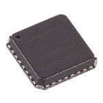
ICGOO电子元器件商城为您提供ADCMP566BCPZ由Analog设计生产,在icgoo商城现货销售,并且可以通过原厂、代理商等渠道进行代购。 ADCMP566BCPZ价格参考¥30.42-¥33.00。AnalogADCMP566BCPZ封装/规格:线性 - 比较器, 带锁销 比较器 补充型,差分,ECL,开路发射极 32-LFCSP(5x5)。您可以下载ADCMP566BCPZ参考资料、Datasheet数据手册功能说明书,资料中有ADCMP566BCPZ 详细功能的应用电路图电压和使用方法及教程。
ADCMP566BCPZ 是 Analog Devices Inc.(ADI)生产的一款高速电压比较器,属于线性比较器类别。该器件主要用于需要快速响应和高精度比较功能的应用场景。

其主要应用场景包括:

1. 高速信号处理系统:可用于检测信号电平是否超过设定阈值,适用于雷达、测试设备和高速数据采集系统中的信号监控。

2. 电源管理系统:用于过压、欠压检测,帮助实现电源监控和保护功能,保障系统稳定运行。

3. 工业控制与自动化:在工业控制系统中,用于对传感器信号进行比较和判断,从而实现自动控制或报警功能。

4. 通信设备:在光通信或无线通信系统中,用于信号强度检测或电平转换,辅助实现信号完整性管理。

5. 汽车电子系统:用于电池管理系统(BMS)或车载传感器信号处理,提供快速、可靠的电压比较功能。

该比较器具有低传播延迟、高精度和宽工作电压范围等优点,适合在对速度和稳定性有较高要求的电子系统中使用。
| 参数 | 数值 |
| 产品目录 | 集成电路 (IC)半导体 |
| CMRR,PSRR(典型值) | 69dB CMRR |
| 描述 | IC COMP DUAL ULTRA-FAST 32LFCSP模拟比较器 Dual Ultrafast VTG |
| 产品分类 | |
| 品牌 | Analog Devices |
| 产品手册 | |
| 产品图片 |
|
| rohs | 符合RoHS无铅 / 符合限制有害物质指令(RoHS)规范要求 |
| 产品系列 | 校验器 IC,Analog Devices ADCMP566BCPZ- |
| 数据手册 | |
| 产品型号 | ADCMP566BCPZ |
| PCN其它 | |
| 产品 | Analog Comparators |
| 产品目录页面 | |
| 产品种类 | 模拟比较器 |
| 传播延迟时间 | 240 ps |
| 传播延迟(最大值) | 0.29ns |
| 供应商器件封装 | 32-LFCSP-VQ(5x5) |
| 偏转电压—最大值 | 5 mV |
| 元件数 | 2 |
| 包装 | 托盘 |
| 商标 | Analog Devices |
| 安装类型 | 表面贴装 |
| 安装风格 | SMD/SMT |
| 封装 | Tray |
| 封装/外壳 | 32-VFQFN 裸露焊盘,CSP |
| 封装/箱体 | LFCSP-32 |
| 工作温度 | -40°C ~ 85°C |
| 工厂包装数量 | 490 |
| 最大功率耗散 | 525 mW |
| 最大工作温度 | + 85 C |
| 最小工作温度 | - 40 C |
| 标准包装 | 1 |
| 比较器类型 | Differential |
| 滞后 | ±1mV |
| 电压-电源,单/双 (±) | ±4.75 V ~ 5.25 V |
| 电压-输入失调(最大值) | 5mV @ -5.2V,5V |
| 电压增益dB | 60 dB |
| 电流-输入偏置(最大值) | 42µA @ -5.2V,5V |
| 电流-输出(典型值) | 30mA |
| 电流-静态(最大值) | 18mA,85mA |
| 电源电压-最大 | 5.25 V |
| 电源电压-最小 | 4.75 V |
| 电源电流 | 18 mA |
| 电源电流—最大值 | 18 mA |
| 类型 | 带锁销 |
| 输入偏压电流—最大 | 42 uA |
| 输出类型 | ECL |
| 通道数量 | 2 Channel |
| 配用 | /product-detail/zh/EVAL-ADCMP566BCPZ/EVAL-ADCMP566BCPZ-ND/1679981 |


- 商务部:美国ITC正式对集成电路等产品启动337调查
- 曝三星4nm工艺存在良率问题 高通将骁龙8 Gen1或转产台积电
- 太阳诱电将投资9.5亿元在常州建新厂生产MLCC 预计2023年完工
- 英特尔发布欧洲新工厂建设计划 深化IDM 2.0 战略
- 台积电先进制程称霸业界 有大客户加持明年业绩稳了
- 达到5530亿美元!SIA预计今年全球半导体销售额将创下新高
- 英特尔拟将自动驾驶子公司Mobileye上市 估值或超500亿美元
- 三星加码芯片和SET,合并消费电子和移动部门,撤换高东真等 CEO
- 三星电子宣布重大人事变动 还合并消费电子和移动部门
- 海关总署:前11个月进口集成电路产品价值2.52万亿元 增长14.8%


PDF Datasheet 数据手册内容提取
Dual Ultrafast Voltage Comparator ADCMP566 FEATURES FUNCTIONAL BLOCK DIAGRAM 250 ps propagation delay input to output 50 ps propagation delay dispersion NONINVERTING Differential ECL compatible outputs INPUT Q OUTPUT Differential latch control ADCMP566 INVERTING Q OUTPUT Robust input protection INPUT Input common-mode range −2.0 V to +3.0 V LATCH ENABLE LATCH ENABLE Input differential range ±5 V INPUT INPUT ESD protection >3 kV HBM, >200 V MM 03633-0-001 Power supply sensitivity > 65 dB Figure 1. 200 ps minimum pulsewidth 5 GHz equivalent input rise time bandwidth GENERAL DESCRIPTION Typical output rise/fall of 165 ps The ADCMP566 is an ultrafast voltage comparator fabricated APPLICATIONS on Analog Devices’ proprietary XFCB process. The device High speed instrumentation features 250 ps propagation delay with less than 35 ps overdrive Scope and logic analyzer front ends dispersion. Overdrive dispersion, a particularly important Window comparators characteristic of high speed comparators, is a measure of the High speed line receivers and signal restoration difference in propagation delay under differing overdrive conditions. Threshold detection Peak detection A fast, high precision differential input stage permits consis- High speed triggers tent propagation delay with a wide variety of signals in the Patient diagnostics common-mode range from −2.0 V to +3.0 V. Outputs are Disk drive read channel detection complementary digital signals fully compatible with ECL 10 K Hand-held test instruments and 10 KH logic families. The outputs provide sufficient drive Zero-crossing detectors current to directly drive transmission lines terminated in 50 Ω Clock drivers to −2 V. A latch input is included, which permits tracking, Automatic test equipment track-and-hold, or sample-and-hold modes of operation. The ADCMP566 is available in a 32-lead LFCSP package. Rev. 0 Information furnished by Analog Devices is believed to be accurate and reliable. However, no responsibility is assumed by Analog Devices for its use, nor for any infringements of patents or other rights of third parties that may result from its use. One Technology Way, P.O. Box 9106, Norwood, MA 02062-9106, U.S.A. Specifications subject to change without notice. No license is granted by implication or otherwise under any patent or patent rights of Analog Devices. Trademarks and Tel: 781.329.4700 www.analog.com registered trademarks are the property of their respective owners. Fax: 781.326.8703 © 2003 Analog Devices, Inc. All rights reserved.
ADCMP566 TABLE OF CONTENTS Specifications.....................................................................................3 Optimizing High Speed Performance........................................9 Absolute Maximum Ratings............................................................5 Comparator Propagation Delay Dispersion..............................9 Thermal Considerations..............................................................5 Comparator Hysteresis..............................................................10 ESD Caution..................................................................................5 Minimum Input Slew Rate Requirement................................10 Pin Configuration and Function Descriptions.............................6 Typical Application Circuits.....................................................11 Timing Information.........................................................................8 Typical Performance Characteristics...........................................12 Application Information..................................................................9 Outline Dimensions.......................................................................14 Clock Timing Recovery...............................................................9 Ordering Guide..........................................................................14 REVISION HISTORY Revision 0: Initial Version Rev. 0 | Page 2 of 16
ADCMP566 SPECIFICATIONS Table 1. ADCMP566 ELECTRICAL CHARACTERISTICS (V = +5.0 V, V = −5.2 V, T = 25°C, unless otherwise noted.) CC EE A Parameter Symbol Condition Min Typ Max Unit DC INPUT CHARACTERISTICS (See Note) Input Common-Mode Range V −2.0 +3.0 V CM Input Differential Voltage −5 +5 V Input Offset Voltage V −5.0 ±1.0 +5.0 mV OS Input Offset Voltage Channel Matching ±1.0 mV Offset Voltage Tempco DV /d 10.0 µV/°C OS T Input Bias Current I −10 +24 +42 µA BC Input Bias Current Tempco 10.0 nA/°C Input Offset Current −8.0 ±0.5 +8.0 µA Input Capacitance C 0.75 pF IN Input Resistance, Differential Mode 100 kΩ Input Resistance, Common Mode 600 kΩ Open Loop Gain 60 dB Common-Mode Rejection Ratio CMRR V = −2.0 V to +3.0 V 69 dB CM Hysteresis ±1.0 mV LATCH ENABLE CHARACTERISTICS Latch Enable Common-Mode Range V −2.0 0 V LCM Latch Enable Differential Input Voltage V 0.4 2.0 V LD Input High Current @ 0.0 V −12 +6 +12 µA Input Low Current @ −2.0 V −12 +6 +12 µA Latch Setup Time t 250 mV overdrive 50 ps S Latch to Output Delay t t 250 mV overdrive 250 ps PLOH, PLOL Latch Pulsewidth t 250 mV overdrive 150 ps PL Latch Hold Time t 250 mV overdrive 75 ps H OUTPUT CHARACTERISTICS Output Voltage—High Level V ECL 50 Ω to −2.0 V −1.06 −0.81 V OH Output Voltage—Low Level V ECL 50 Ω to −2.0 V −1.95 −1.65 V OL Rise Time t 20% to 80% 170 ps R Fall Time t 20% to 80% 140 ps F AC PERFORMANCE Propagation Delay t 1 V overdrive 240 ps PD Propagation Delay t 20 mV overdrive 290 ps PD Propagation Delay Tempco 0.5 ps/°C Prop Delay Skew—Rising Transition to ±10 ps Falling Transition Within Device Propagation Delay Skew— ±10 ps Channel to Channel Propagation Delay Dispersion vs. 1 MHz, 1 ns t, t ±10 ps R F Duty Cycle Propagation Delay Dispersion vs. 50 mV to 1.5 V 35 ps Overdrive Propagation Delay Dispersion vs. 20 mV to 1.5 V 50 ps Overdrive Propagation Delay Dispersion vs. 0 V to 1 V swing, 50 ps Slew Rate 20% to 80%, 50 and 600 ps t, t R F Propagation Delay Dispersion vs. 1 V swing, 5 ps Common-Mode Voltage −1.5 V to 2.5 V CM Equivalent Input Rise Time Bandwidth BW 0 V to 1 V swing, 5000 MHz 20% to 80%, 50 ps t, t R F Rev. 0 | Page 3 of 16
ADCMP566 Parameter Symbol Condition Min Typ Max Unit AC PERFORMANCE (continued) Toggle Rate >50% output swing 5 Gbps Minimum Pulsewidth PW ∆t from 10 ns to 200 ps pd 200 ps < ±25 ps Unit to Unit Propagation Delay Skew ±10 ps POWER SUPPLY Positive Supply Current I @ +5.0 V 9 13 18 mA VCC Negative Supply Current I @ −5.2 V 60 70 85 mA VEE Positive Supply Voltage V Dual 4.75 5.0 5.25 V CC Negative Supply Voltage V Dual −4.96 −5.2 −5.45 V EE Power Dissipation Dual, without load 375 450 525 mW Power Dissipation Dual, with load 550 mW Power Supply Sensitivity—V PSS 68 dB CC VCC Power Supply Sensitivity—V PSS 85 dB EE VEE NOTE: Under no circumstances should the input voltages exceed the supply voltages. Rev. 0 | Page 4 of 16
ADCMP566 ABSOLUTE MAXIMUM RATINGS Table 2. ADCMP566 Absolute Maximum Ratings THERMAL CONSIDERATIONS Parameter Rating The ADCMP566 LFCSP 32-lead package option has a θ Supply Positive Supply Voltage −0.5 V to +6.0 V JA (junction-to-ambient thermal resistance) of 27.2°C/W in Voltages (VCC to GND) still air. Negative Supply Voltage −6.0 V to +0.5 V (V to GND) EE Ground Voltage Differential −0.5 V to +0.5 V Input Input Common-Mode −3.0 V to +4.0 V Voltages Voltage Differential Input Voltage −7.0 V to +7.0 V Input Voltage, V to 0.5 V EE Latch Controls Output Output Current 30 mA Temperature Operating Temperature, −40°C to +85°C Ambient Operating Temperature, 125°C Junction Storage Temperature Range −65°C to +150°C Stress above those listed under Absolute Maximum Ratings may cause permanent damage to the device. This is a stress rating only and functional operation of the device at these or any other conditions above those indicated in the operational sections of this specification is not implied. Exposure to absolute maximum rating conditions for extended periods may affect device reliability. ESD CAUTION ESD (electrostatic discharge) sensitive device. Electrostatic charges as high as 4000 V readily accumulate on the human body and test equipment and can discharge without detection. Although this product features proprietary ESD protection circuitry, permanent damage may occur on devices subjected to high energy electrostatic discharges. Therefore, proper ESD precautions are recommended to avoid performance degradation or loss of functionality. Rev. 0 | Page 5 of 16
ADCMP566 PIN CONFIGURATION AND FUNCTION DESCRIPTIONS DAA D D NEECNAAN GLLNGQQG 21098765 33322222 GND1 PIN 1 24VEE –INA2 23NC INDICATOR +INA3 22VEE VCC4 ADCMP566 21VCC VCC5 TOP VIEW 20VCC +INB6 (Not to Scale) 19VEE –INB7 18NC GND8 17VEE 90123456 1111111 DBBCDBBD NEENNQQN GLL G G NC = NO CONNECT 03633-0-002 Figure 2. ADCMP566 Pin Configuration Table 3. ADCMP566 Pin Descriptions Pin No. Mnemonic Function 1 GND Analog Ground 2 −INA Inverting analog input of the differential input stage for Channel A. The inverting A input must be driven in conjunction with the noninverting A input. 3 +INA Noninverting analog input of the differential input stage for Channel A. The noninverting A input must be driven in conjunction with the inverting A input. 4 V Positive Supply Terminal CC 5 V Positive Supply Terminal CC 6 +INB Noninverting analog input of the differential input stage for Channel B. The noninverting B input must be driven in conjunction with the inverting B input. 7 −INB Inverting analog input of the differential input stage for Channel B. The inverting B input must be driven in conjunction with the noninverting B input. 8 GND Analog Ground 9 GND Analog Ground 10 LEB One of two complementary inputs for Channel B Latch Enable. In the compare mode (logic low), the output will track changes at the input of the comparator. In the latch mode (logic high), the output will reflect the input state just prior to the comparator’s being placed in the latch mode. LEB must be driven in conjunction with LEB. 11 LEB One of two complementary inputs for Channel B Latch Enable. In the compare mode (logic high), the output will track changes at the input of the comparator. In the latch mode (logic low), the output will reflect the input state just prior to the comparator’s being placed in the latch mode. LEB must be driven in conjunction with LEB. 12 NC No Connect. Leave pin unconnected. 13 GND Digital Ground 14 QB One of two complementary outputs for Channel B. QB will be at logic low if the analog voltage at the noninverting input is greater than the analog voltage at the inverting input (provided the comparator is in the compare mode). See the LEB description (Pin 11) for more information. 15 QB One of two complementary outputs for Channel B. QB will be at logic high if the analog voltage at the noninverting input is greater than the analog voltage at the inverting input (provided the comparator is in the compare mode). See the LEB description (Pin 11) for more information. 16 GND Digital Ground 17 V Negative Supply Terminal EE 18 NC No Connect. Leave pin unconnected. 19 V Negative Supply Terminal EE 20 V Positive Supply Terminal CC 21 V Positive Supply Terminal CC Rev. 0 | Page 6 of 16
ADCMP566 Pin No. Mnemonic Function 22 V Negative Supply Terminal EE 23 NC No Connect. Leave pin unconnected. 24 V Negative Supply Terminal EE 25 GND Digital Ground 26 QA One of two complementary outputs for Channel A. QA will be at logic high if the analog voltage at the noninverting input is greater than the analog voltage at the inverting input (provided the comparator is in the compare mode). See the LEA description (Pin 30) for more information. 27 QA One of two complementary outputs for Channel A. QA will be at logic low if the analog voltage at the noninverting input is greater than the analog voltage at the inverting input (provided the comparator is in the compare mode). See the LEA description (Pin 30) for more information. 28 GND Digital Ground 29 NC No Connect. Leave pin unconnected. 30 LEA One of two complementary inputs for Channel A Latch Enable. In the compare mode (logic high), the output will track changes at the input of the comparator. In the latch mode (logic low), the output will reflect the input state just prior to the comparator’s being placed in the latch mode. LEA must be driven in conjunction with LEA. 31 LEA One of two complementary inputs for Channel A Latch Enable. In the compare mode (logic low), the output will track changes at the input of the comparator. In the latch mode (logic high), the output will reflect the input state just prior to the comparator’s being placed in the latch mode. LEA must be driven in conjunction with LEA. 32 GND Analog Ground Rev. 0 | Page 7 of 16
ADCMP566 TIMING INFORMATION LATCH ENABLE 50% LATCH ENABLE tS tPL t H DIFFERENTIAL VIN INPUT VOLTAGE VOD VREF± VOS t t PDL PLOH Q OUTPUT 50% t t F PDH 50% Q OUTPUT t PLOL t R 03633-0-003 Figure 3. System Timing Diagram Symbol Timing Description The timing diagram in Figure 3 shows the ADCMP566 compare t Minimum Minimum time after the negative and latch features. Table 4 describes the terms in the diagram. H hold time transition of the Latch Enable Table 4. Timing Descriptions signal that the input signal must Symbol Timing Description remain unchanged to be acquired and held at the outputs t Input to output Propagation delay measured from PDH high delay the time the input signal crosses tPL Minimum Minimum time that the Latch the reference (± the input offset latch enable Enable signal must be high to voltage) to the 50% point of an pulsewidth acquire an input signal change output low-to-high transition t Minimum Minimum time before the S t Input to output Propagation delay measured from setup time negative transition of the Latch PDL low delay the time the input signal crosses Enable signal that an input signal the reference (± the input offset change must be present to be voltage) to the 50% point of an acquired and held at the outputs output high-to-low transition t Output rise Amount of time required to R t Latch enable Propagation delay measured from time transition from a low to a high PLOH to output high the 50% point of the Latch Enable output as measured at the 20% delay signal low-to-high transition to and 80% points the 50% point of an output low- t Output fall Amount of time required to F to-high transition time transition from a high to a low t Latch enable Propagation delay measured from output as measured at the 20% PLOL to output low the 50% point of the Latch Enable and 80% points delay signal low-to-high transition to V Voltage Difference between the OD the 50% point of an output high- overdrive differential input and reference to-low transition input voltages Rev. 0 | Page 8 of 16
ADCMP566 APPLICATION INFORMATION The ADCMP566 comparators are very high speed devices. CLOCK TIMING RECOVERY Consequently, high speed design techniques must be employed Comparators are often used in digital systems to recover clock to achieve the best performance. The most critical aspect of any timing signals. High speed square waves transmitted over a ADCMP566 design is the use of a low impedance ground plane. distance, even tens of centimeters, can become distorted due to A ground plane, as part of a multilayer board, is recommended stray capacitance and inductance. Poor layout or improper for proper high speed performance. Using a continuous termination can also cause reflections on the transmission line, conductive plane over the surface of the circuit board can create further distorting the signal waveform. A high speed this, allowing breaks in the plane only for necessary signal comparator can be used to recover the distorted waveform paths. The ground plane provides a low inductance ground, while maintaining a minimum of delay. eliminating any potential differences at different ground points throughout the circuit board caused by ground bounce. A OPTIMIZING HIGH SPEED PERFORMANCE proper ground plane also minimizes the effects of stray As with any high speed comparator amplifier, proper design and capacitance on the circuit board. layout techniques should be used to ensure optimal perform- ance from the ADCMP566. The performance limits of high It is also important to provide bypass capacitors for the power speed circuitry can easily be a result of stray capacitance, supply in a high speed application. A 1µF electrolytic bypass improper ground impedance, or other layout issues. capacitor should be placed within 0.5 inches of each power supply pin to ground. These capacitors will reduce any potential Minimizing resistance from source to the input is an important voltage ripples from the power supply. In addition, a 10 nF consideration in maximizing the high speed operation of the ceramic capacitor should be placed as close as possible from the ADCMP566. Source resistance in combination with equivalent power supply pins on the ADCMP566 to ground. These input capacitance could cause a lagged response at the input, capacitors act as a charge reservoir for the device during high thus delaying the output. The input capacitance of the frequency switching. ADCMP566 in combination with stray capacitance from an input pin to ground could result in several picofarads of The LATCH ENABLE input is active low (latched). If the equivalent capacitance. A combination of 3 kΩ source resistance latching function is not used, the LATCH ENABLE input and 5 pF of input capacitance yields a time constant of 15 ns, should be grounded (ground is an ECL logic high), and the which is significantly slower than the sub 500 ps capability of complementary input, LATCH ENABLE, should be tied to the ADCMP566. Source impedances should be significantly less −2.0 V. This will disable the latching function. than 100 Ω for best performance. Occasionally, one of the two comparator stages within the Sockets should be avoided due to stray capacitance and induc- ADCMP566 will not be used. The inputs of the unused tance. If proper high speed techniques are used, the ADCMP566 comparator should not be allowed to float. The high internal should be free from oscillation when the comparator input gain may cause the output to oscillate (possibly affecting the signal passes through the switching threshold. comparator that is being used) unless the output is forced into a fixed state. This is easily accomplished by ensuring that the two COMPARATOR PROPAGATION inputs are at least one diode drop apart, while also appropriately DELAY DISPERSION connecting the LATCH ENABLE and LATCH ENABLE inputs The ADCMP566 has been specifically designed to reduce as described above. propagation delay dispersion over an input overdrive range of 100 mV to 1 V. Propagation delay overdrive dispersion is the The best performance is achieved with the use of proper ECL change in propagation delay that results from a change in the terminations. The open emitter outputs of the ADCMP566 are degree of overdrive (how far the switching point is exceeded by designed to be terminated through 50 Ω resistors to −2.0 V, or the input). The overall result is a higher degree of timing any other equivalent ECL termination. If a −2.0 V supply is not accuracy since the ADCMP566 is far less sensitive to input available, an 82 Ω resistor to ground and a 130 Ω resistor to variations than most comparator designs. −5.2 V provide a suitable equivalent. If high speed ECL signals must be routed more than a centimeter, microstrip or stripline Propagation delay dispersion is a specification that is important techniques may be required to ensure proper transition times in critical timing applications such as ATE, bench instruments, and prevent output ringing. and nuclear instrumentation. Overdrive dispersion is defined Rev. 0 | Page 9 of 16
ADCMP566 as the variation in propagation delay as the input overdrive –VH +VH conditions are changed (Figure 4). For the ADCMP566, 2 2 0V overdrive dispersion is typically 35 ps as the overdrive is INPUT changed from 100 mV to 1 V. This specification applies for 1 both positive and negative overdrive since the ADCMP566 has equal delays for positive and negative going inputs. The 35 ps propagation delay overdrive dispersion of the ADCMP566 offers considerable improvement of the 100 ps dispersion of other similar series comparators. 0 1.5V OVERDRIVE INPUT VOLTAGE OUTPUT 20mV OVERDRIVE 03633-0-005 VREF± VOS Figure 5. Comparator Hysteresis Transfer Function DISPERSION 60 Q OUTPUT 50 03633-0-004 Figure 4. Propagation Delay Dispersion 40 V) m COMPARATOR HYSTERESIS S ( SI 30 E R The addition of hysteresis to a comparator is often useful in a E T S noisy environment or where it is not desirable for the compara- Y 20 H tor to toggle between states when the input signal is at the switching threshold. The transfer function for a comparator 10 with hysteresis is shown in Figure 5. If the input voltage acpomprpoaarcahteosr twhiel lt hswreistchho lfdr ofmro ma 0t htoe na e1g wathiveen d tihree citniponut, tchreo sses 0–20 –15 –1∆0 LATCH–5 = LE– L0EB (mV)5 10 15 03633-0-006 +VH/2. The new switching threshold becomes −VH/2. The Figure 6. Comparator Hysteresis Transfer Function comparator will remain in a 1 state until the threshold −V /2 is Using Latch Enable Input H crossed coming from the positive direction. In this manner, noise centered on 0 V input will not cause the comparator to MINIMUM INPUT SLEW RATE REQUIREMENT switch states unless it exceeds the region bounded by ±V /2. H As for all high speed comparators, a minimum slew rate must Positive feedback from the output to the input is often used to be met to ensure that the device does not oscillate when the produce hysteresis in a comparator (Figure 9). The major input crosses the threshold. This oscillation is due in part to the problem with this approach is that the amount of hysteresis high input bandwidth of the comparator and the parasitics of varies with the output logic levels, resulting in a hysteresis that the package. Analog Devices recommends a slew rate of 5 V/µs is not symmetrical around zero. or faster to ensure a clean output transition. If slew rates less than 5 V/µs are used, then hysteresis should be added to reduce Another method to implement hysteresis is generated by the oscillation. introducing a differential voltage between LATCH ENABLE and LATCH ENABLE. inputs (Figure 10). Hysteresis generated in this manner is independent of output swing and is symmetri- cal around zero. The variation of hysteresis with input voltage is shown in Figure 6. Rev. 0 | Page 10 of 16
ADCMP566 TYPICAL APPLICATION CIRCUITS VIN VIN ADCMP566 OUTPUTS ADCMP566 OUTPUTS VREF LATCH –2.0V HYSTERESIS 450Ω –2.0V ENABLE VOLTAGE INPUTS ALL RESISTORS 50Ω ALL RESISTORS 50Ω UNLESS OTHERWISE NOTED 03633-0-007 03633-0-010 Figure 7. High Speed Sampling Circuits Figure 10. Hysteresis Using Latch Enable Input +VREF 30Ω 50Ω ADCMP566 OUTPUTS VIN ADCMP566 VIN 30Ω 50Ω 127Ω 127Ω –5.2V 03633-0-011 ADCMP566 Figure 11. How to Interface an ECL Output to an –VREF Instrument with a 50 Ω to Ground Input LATCH –2.0V ENABLE INPUTS ALL RESISTORS 50Ω 03633-0-008 Figure 8. High Speed Window Comparator VIN ADCMP566 OUTPUTS VREF R1 R2 –2.0V ALL RESISTORS 50Ω 03633-0-009 Figure 9. Hysteresis Using Positive Feedback Rev. 0 | Page 11 of 16
ADCMP566 TYPICAL PERFORMANCE CHARACTERISTICS (V = +5.0 V, V = −5.2 V, T = 25°C, unless otherwise noted.) CC EE A 30 23.4 25 23.2 A) µ RENT (A)µ 20 URRENT (N = 0V)2223..80 UT BIAS CUR 1105 NPUT BIAS C(+IN = 1V,–I2222..64 NP N I I 5 +I 22.2 –02N.O5NINVE–R1T.5ING INP–U0T.5 VOLTAG0.E5 (INVERT1.I5NG VOLT2A.5GE = 0.5V3).5 03633-0-013 22.0–40 Figu–r2e0 15. Inpu0tT BEiMasP ECRu2Ar0rTeUnRt Ev s(.° 4CT0e)mpera6tu0re 80 03633-0-016 Figure 12. Input Bias Current vs. Input Voltage 60 2.0 1.8 50 1.6 mV) 1.4 mV) 40 T VOLTAGE ( 110...208 YSTERESIS ( 2300 E H S F 0.6 F O 0.4 10 0.2 0–40 –20 0TEMPER2A0TURE (°4C0) 60 80 03633-0-014 0–20 –15 Fig–u1r∆0e L1A6T. CHH–y5 s=t eLrEes–i sL0 EvsB. (∆mLVa)t5ch 10 15 03633-0-017 Figure 13. Input Offset Voltage vs. Temperature 195 195 185 185 175 175 E (ps) 165 ME (ps) 165 TIM 155 TI 155 145 145 135 135 125–40 –30 –20 –10 0 TE1M0PE2R0ATU30RE 4(°0C) 50 60 70 80 90 03633-0-015 125–40 –30 –2F0ig–u1r0e 107. TFEa1Ml0l PTEim2R0Ae TvU3s0.R TEe m4(°0Cp)e5ra0tur6e0 70 80 90 03633-0-018 Figure 14. Rise Time vs. Temperature Rev. 0 | Page 12 of 16
ADCMP566 242 239 240 238 s) 238 s) 237 p p AY ( 236 AY ( 236 L L E E D D N 234 N 235 O O TI TI GA 232 GA 234 A A P P RO 230 RO 233 P P 228 232 226–40 –30 –20 –10 0 TE1M0PE2R0ATU30RE 4(°0C) 50 60 70 80 90 03633-0-019 231–2 –I1NPUT COMM0ON-MODE V1OLTAGE (V)2 3 03633-0-022 Figure 18. Propagation Delay vs. Temperature Figure 21. Propagation Delay vs. Common-Mode Voltage 60 0 –5 s) 50 s) p p R ( R ( –10 O O R 40 R R R –15 E E Y Y A A L 30 L –20 E E D D N N O O –25 TI 20 TI A A G G A A –30 P P RO 10 RO P P –35 00 0.2 0.4OVE0R.6DRIVE0 V.8OLTA1G.E0 (V) 1.2 1.4 1.6 03633-0-020 –400.15 2.15 P4U.1L5SEWIDTH6 (.n1s5) 8.15 03633-0-023 Figure 19. Propagation Delay Error vs. Overdrive Voltage Figure 22. Propagation Delay Error vs. Pulsewidth –0.8 –1.0 V) LL ( –1.2 A F D N A –1.4 E S RI UT –1.6 P T U O –1.8 –2.01.0 1.1 1.2 1.3 1.4TIM1E. 5(ns)1.6 1.7 1.8 1.9 2.0 03633-0-021 Figure 20. Rise and Fall of Outputs vs. Time Rev. 0 | Page 13 of 16
ADCMP566 OUTLINE DIMENSIONS 5.00 0.60 MAX BSC SQ 0.60 MAX PIN 1 INDICATOR 2425 321 PIN 1 INDICATOR 0.50 TOP 4.75 BSC BOTTOM 3.25 VIEW BSC SQ VIEW 2.70SQ 1.25 0.50 00..4300 1716 98 0.80 MAX 3.50 12° MAX 0.65 NOM REF 0.05 MAX 1.00 0.02 NOM 0.90 0.30 0.80 SEATING 00..2138 0.20 REF COPL0A.0N8ARITY PLANE COMPLIANT TO JEDEC STANDARDS MO-220-VHHD-2 Figure 23. 32-Lead Lead Frame Chip Scale Package [LFCSP] (CP-32) Dimensions shown in millimeters ORDERING GUIDE Model Temperature Range Package Description Package Option ADCMP566BCP −40°C to +85°C LFCSP-32 CP-32 Rev. 0 | Page 14 of 16
ADCMP566 Notes Rev. 0 | Page 15 of 16
ADCMP566 Notes © 2003 Analog Devices, Inc. All rights reserved. Trademarks and registered trademarks are the property of their respective owners. C03633–0–10/03(0) Rev. 0 | Page 16 of 16
Mouser Electronics Authorized Distributor Click to View Pricing, Inventory, Delivery & Lifecycle Information: A nalog Devices Inc.: EVAL-ADCMP566BCPZ ADCMP566BCPZ