
 Datasheet下载
- 型号: MAX9100EUK+T
- 制造商: Maxim
- 库位|库存: xxxx|xxxx
- 要求:
| 数量阶梯 | 香港交货 | 国内含税 |
| +xxxx | $xxxx | ¥xxxx |
查看当月历史价格
查看今年历史价格
MAX9100EUK+T产品简介:
ICGOO电子元器件商城为您提供MAX9100EUK+T由Maxim设计生产,在icgoo商城现货销售,并且可以通过原厂、代理商等渠道进行代购。 MAX9100EUK+T价格参考。MaximMAX9100EUK+T封装/规格:线性 - 比较器, Comparator General Purpose CMOS, Push-Pull, Rail-to-Rail, TTL SOT-23-5。您可以下载MAX9100EUK+T参考资料、Datasheet数据手册功能说明书,资料中有MAX9100EUK+T 详细功能的应用电路图电压和使用方法及教程。
Maxim Integrated的MAX9100EUK+T是一款低功耗、高速电压比较器,属于线性比较器类别。该器件采用微型SC70封装,适用于对空间和功耗敏感的应用场景。

其典型应用场景包括便携式电子设备中的电池管理与电压监控,如智能手机、平板电脑和可穿戴设备,用于检测电池电量或电源状态并触发低电压警告。由于其响应速度快(传播延迟仅约6.5ns),也适用于需要快速信号判断的系统,例如过压/欠压保护电路、脉冲宽度检测和数据采样系统。

此外,MAX9100EUK+T工作电压范围宽(1.7V至5.5V),支持单电源或双电源工作,适合多电压轨系统的电平转换与逻辑接口应用,常见于工业传感器、消费类电子产品和小型嵌入式系统中。其低静态电流(典型值24μA)使其非常适合电池供电的长期运行设备。

综上,MAX9100EUK+T广泛应用于便携设备、电源监控、工业控制及信号调理等需要高精度、低功耗和小尺寸封装的场合。
| 参数 | 数值 |
| 产品目录 | 集成电路 (IC)半导体 |
| CMRR,PSRR(典型值) | 68dB CMRR,66dB PSRR |
| 描述 | IC COMPARATOR R-R SOT23-5Comparator ICs 1.0V uPower Comparator |
| 产品分类 | |
| 品牌 | Maxim Integrated |
| 产品手册 | |
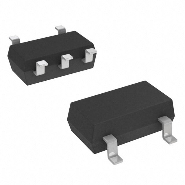
| 产品图片 |
|
| rohs | 符合RoHS无铅 / 符合限制有害物质指令(RoHS)规范要求 |
| 产品系列 | 校验器 IC,Maxim Integrated MAX9100EUK+T- |
| 数据手册 | |
| 产品型号 | MAX9100EUK+T |
| 产品 | Analog Comparators |
| 产品培训模块 | http://www.digikey.cn/PTM/IndividualPTM.page?site=cn&lang=zhs&ptm=25703http://www.digikey.cn/PTM/IndividualPTM.page?site=cn&lang=zhs&ptm=25705 |
| 产品目录页面 | |
| 产品种类 | 校验器 IC |
| 传播延迟(最大值) | 4.5µs |
| 供应商器件封装 | SOT-23-5 |
| 偏转电压—最大值 | 10 mV |
| 元件数 | 1 |
| 其它名称 | MAX9100EUK+T-ND |
| 包装 | 带卷 (TR) |
| 商标 | Maxim Integrated |
| 安装类型 | 表面贴装 |
| 安装风格 | SMD/SMT |
| 封装 | Reel |
| 封装/外壳 | SC-74A,SOT-753 |
| 封装/箱体 | SOT-23-5 |
| 工作温度 | -40°C ~ 85°C |
| 工厂包装数量 | 2500 |
| 最大功率耗散 | 571 mW |
| 最大工作温度 | + 85 C |
| 最小工作温度 | - 40 C |
| 标准包装 | 2,500 |
| 比较器类型 | General Purpose |
| 滞后 | ±2mV |
| 电压-电源,单/双 (±) | 1 V ~ 5.5 V |
| 电压-输入失调(最大值) | 10mV @ 5.5V |
| 电流-输入偏置(最大值) | 0.015µA @ 5.5V |
| 电流-输出(典型值) | - |
| 电流-静态(最大值) | 13µA |
| 电源电压-最大 | 5.5 V |
| 电源电压-最小 | 1 V |
| 电源电流 | 13 uA |
| 电源电流—最大值 | 13 uA |
| 类型 | 通用 |
| 系列 | MAX9100 |
| 输入偏压电流—最大 | 0.015 uA |
| 输出类型 | Push-Pull |
| 通道数量 | 1 Channel |
| 零件号别名 | MAX9100 |


- 商务部:美国ITC正式对集成电路等产品启动337调查
- 曝三星4nm工艺存在良率问题 高通将骁龙8 Gen1或转产台积电
- 太阳诱电将投资9.5亿元在常州建新厂生产MLCC 预计2023年完工
- 英特尔发布欧洲新工厂建设计划 深化IDM 2.0 战略
- 台积电先进制程称霸业界 有大客户加持明年业绩稳了
- 达到5530亿美元!SIA预计今年全球半导体销售额将创下新高
- 英特尔拟将自动驾驶子公司Mobileye上市 估值或超500亿美元
- 三星加码芯片和SET,合并消费电子和移动部门,撤换高东真等 CEO
- 三星电子宣布重大人事变动 还合并消费电子和移动部门
- 海关总署:前11个月进口集成电路产品价值2.52万亿元 增长14.8%


PDF Datasheet 数据手册内容提取
19-1808; Rev 1; 1/07 +1.0V Micropower SOT23 Comparators General Description ____________________________Features M The MAX9100/MAX9101 micropower comparators are • Ultra-Low Voltage: Guaranteed Down to 1.0V A optimized for single-cell systems, and are fully speci- • Low Quiescent Current: 5µA X fied for operation from a single supply of 1.0V to 5.5V. This ultra-low voltage operation, 5µA quiescent current • Optimized for Single-Cell Battery-Powered 9 consumption, and small footprint make the Systems 1 MAX9100/MAX9101 ideal for use in battery-powered • Wide Input Common-Mode Range 0 systems. A wide-input common-mode range that includes the negative rail and rail-to-rail output swing • CMOS Rail-to-Rail Output Swing (MAX9100) 0 allows almost all of the power supply to be used for sig- • Open-Drain Output (MAX9101) /M nal voltage. In addition, propagation delay is less than • 4µs Propagation Delay 4µs, and rise and fall times are 100ns. A The MAX9100 features a push-pull CMOS output stage • High Output Drive Capability: 5mA Sink and X that sinks and sources current with large internal output Source (MAX9100) 9 drivers that allow rail-to-rail output swings with loads up • No Output Phase Reversal for Overdriven Inputs 1 to 5mA.The MAX9101 has an open-drain output stage that makes it suitable for mixed-voltage designs. • Available in Tiny SOT23-5 Package 0 1 The MAX9100/MAX9101 are available in tiny SOT23-5 packages. ________________________Applications Ordering Information Single-Cell Systems PIN- TOP PKG PART Pagers PACKAGE MARK CODE Closed Sensor Applications MAX9100EUK-T 5 SOT23-5 ADOR U5-1 MAX9100ESA 8 SO — S8-2 Battery-Powered Instrumentation MAX9101EUK-T 5 SOT23-5 ADOS U5-1 Portable Electronic Equipment MAX9101ESA 8 SO — S8-2 Portable Communication Devices Note: All devices specified for over -40°C to +85°C operating temperature range. Typical Operating Characteristic Pin Configurations SUPPLY CURRENT vs. TEMPERATURE 78 VCC = +5V MAX9100 toc01 TOP VIEW 6 OUT 1 5 VCC VCC = +2V A) µ (CC 5 GND 2 MMAAXX99110001 I VCC = +1V 4 IN+ 3 4 IN- 3 SOT23 2 -40 -15 10 35 60 85 TEMPERATURE (°C) Pin Configurations continued at end of data sheet. ________________________________________________________________Maxim Integrated Products 1 For pricing, delivery, and ordering information,please contact Maxim/Dallas Direct!at 1-888-629-4642, or visit Maxim’s website at www.maxim-ic.com.
+1.0V Micropower SOT23 Comparators 1 ABSOLUTE MAXIMUM RATINGS 0 Supply Voltage (VCCto GND).................................-0.3V to +6V 8-Pin Plastic SO 1 IN+ or IN- to GND......................................-0.3V to (VCC+ 0.3V) (derate 5.88mW/°C above +70°C).............................471mW Current Into Input Pins.....................................................±20mA Operating Temperature Range..........................-40°C to +85°C 9 Output Voltages to GND Junction Temperature.....................................................+150°C X MAX9100..............................................-0.3V to (VCC+ 0.3V) Storage Temperature Range............................-65°C to +150°C MAX9101............................................................-0.3V to +6V Lead Temperature (soldering, 10s).................................+300°C A Output Short-Circuit Duration (to VCCor GND).........Continuous M Continuous Power Dissipation (TA= +70°C) 5-Pin Plastic SOT23 / (derate 7.3mW/°C above +70°C)...............................571mW 0 0 Stresses beyond those listed under “Absolute Maximum Ratings” may cause permanent damage to the device. These are stress ratings only, and functional 1 operation of the device at these or any other conditions beyond those indicated in the operational sections of the specifications is not implied. Exposure to 9 absolute maximum rating conditions for extended periods may affect device reliability. X A ELECTRICAL CHARACTERISTICS M (VCC= +1.2V to +5.5V, VCM= 0V, and TA= TMINto TMAX, unless otherwise noted. Typical values are at TA= +25°C.) (Note 1) PARAMETER SYMBOL CONDITIONS MIN TYP MAX UNITS Supply Voltage Range VCC Inferred from the PSRR tests 1.0 5.5 V VCC = +1V, TA = +25°C 5.0 8.0 Supply Current ICC µA VCC = +5V, TA = TMIN to TMAX 6.0 13.0 TA = +25°C ±3 ±10 Input Offset Voltage VOS TA = TMIN to TMAX ±20 mV Input Hysteresis VHYST ±2 mV VCC = +5.5V, TA = +25°C ±0.1 ±5 Input Offset Current IOS nA VCC = +5.5V, TA = TMIN to TMAX ±10 VCC = +5.5V, TA = +25°C ±5 ±15 Input Bias Current IB nA VCC = +5.5V, TA = TMIN to TMAX ±30 Differential mode 200 Input Resistance RIN MΩ Common mode 65 Input Common-Mode Voltage Range (Note 2) VCM Inferred from CMRR test 0 V C C - 0.2 V Common-Mode TA = +25°C 54 68 CMRR dB Rejection Ratio (Note 3) TA = TMIN to TMAX 46 Power-Supply 1.0V ≤ VCC ≤ 1.5V, TA = +25°C 54 66 PSRR dB Rejection Ratio 1.5V ≤ VCC ≤ 5.5V, TA = -40°C to +85°C 56 68 VCC = +5.0V, ISOURCE = 5mA 90 180 VCC = +1.2V, ISOURCE = 0.5mA 60 120 Output-Voltage High (MAX9100) VC C - VO H mV VCC = +1.0V, ISOURCE = 0.1mA, 25 75 TA = +25°C VCC = +5.0V, ISINK = 5mA 100 180 Output-Voltage Low VOL VCC = +1.2V, ISINK = 0.5mA 45 120 mV VCC = +1.0V, ISINK = 0.5mA, TA = +25°C 15 75 2 _______________________________________________________________________________________
+1.0V Micropower SOT23 Comparators ELECTRICAL CHARACTERISTICS (continued) M (VCC= +1.2V to +5.5V, VCM= 0V, and TA= TMINto TMAX, unless otherwise noted. Typical values are at TA= +25°C.) (Note 1) A PARAMETER SYMBOL CONDITIONS MIN TYP MAX UNITS X Sourcing VCC = +5.0V 25 9 (MAX9100) VCC = +1.2V 3 1 Output Short-Circuit Current ISC mA VCC = +5.0V 28 0 Sinking VCC = +1.2V 3 0 Output Open-Drain Leakage / ILKG VCC = +5.5V 0.02 0.2 µA M Current (MAX9101) Power-Up Time tPU 250 ns A Input Capacitance CIN 3 pF X Output Rise Time (MAX9100) trise CL = 15pF 100 ns 9 Output Fall Time (Note 4) tfall CL = 15pF 100 ns 1 tpd+ VOVERDRIVE = 50mV, VCC = +5.0V 3.4 0 tpd- VOVERDRIVE = 50mV, VCC = +5.0V 4.5 1 Propagation Delay (Note 5) µs tpd+ VOVERDRIVE = 50mV, VCC = +1.0V 3.3 tpd- VOVERDRIVE = 50mV, VCC = +1.0V 3.7 Note 1: All specifications are 100% production tested at TA= +25°C. All temperature limits are guaranteed by design. Note 2: Operation with VCMup to VCCis possible with reduced accuracy. See the Input Stage CircuitryandRail-to-Rail Operationsection. Note 3: Tested over the specified Input Common-Mode Voltage Range and with VCC= +5.5V. Note 4: Specified with CL= 15pF for MAX9100/MAX9101, and with RPULLUP= 5kΩfor MAX9101. Note 5: Input overdrive is defined above and beyond the offset voltage and hysteresis of the comparator input. _______________________________________________________________________________________ 3
+1.0V Micropower SOT23 Comparators 1 Typical Operating Characteristics 0 (VCC= +5V, VCM= 0V, TA= +25°C, unless otherwise noted.) 1 9 OUTPUT-VOLTAGE LOW OUTPUT-VOLTAGE HIGH X SUPPLY CURRENT vs. TEMPERATURE vs. SINK CURRENT vs. SOURCE CURRENT MA 78 VCC = +5V MAX9100 toc01 560000 MAX1900 toc02 560000 MAX1900 toc03 / VCC = +1V 0 6 VCC = +2V 400 VCC = +1V V) 400 0 µA) mV) (mH VCC = +2V 91 I (CC 45 VCC = +1V V (OL230000 VCC = +1.2V VCC = +2V VCC = +5V V- VCC O230000 VCC = +1.2V VCC = +5V X 3 100 100 A M 2 0 0 -40 -15 10 35 60 85 0 5 10 15 20 0 5 10 15 20 TEMPERATURE (°C) ILOAD (mA) ILOAD (mA) SUPPLY CURRENT INPUT BIAS CURRENT vs. VCM SUPPLY CURRENT vs. SUPPLY VOLTAGE vs. OUTPUT TRANSITION FREQUENCY 789000000 MAX9100 toc04 77..05 VOUT = VCC MAX9100 toc05 433050 VCC = +5V MAX9100 toc06 600 6.5 500 25 I (nA)BIAS340000 µI (A)CC 6.0 µI (A)CC 20 15 200 5.5 VOUT = GND VCC = +2V 100 IBIAS(-) = IBIAS(+) 10 5.0 0 5 VCM = VCC VCC = +1V -100 4.5 0 0 1 2 3 4 5 1 2 3 4 5 0.01 0.1 1 10 100 VCM (V) VCC (V) fCLK (kHz) PROPAGATION DELAY (tpd+) PROPAGATION DELAY (tpd+) PROPAGATION DELAY (tpd)+ vs. INPUT OVERDRIVE vs. INPUT OVERDRIVE vs. INPUT OVERDRIVE 45..50 MAX9100 toc07 45..50 MAX9100 toc08 45..50 MAX9100 toc09 µs) µs) µs) Y ( Y ( Y ( TION DELA 4.0 TION DELA 4.0 TA = +T8A5 =° C+25°C TION DELA 4.0 TA = -40°C TA = +85°C AGA 3.5 TA = +85°C AGA 3.5 AGA 3.5 P P P O O O R R R P P P 3.0 3.0 TA = -40°C 3.0 TA = +25°C VCC = +5V TA = +25°C, -40°C VCC = +2V VCC = +1V 2.5 2.5 2.5 0 50 100 150 200 250 0 20 40 60 80 100 0 20 40 60 80 100 VOD (mV) VOD (mV) VOD (mV) 4 _______________________________________________________________________________________
+1.0V Micropower SOT23 Comparators Typical Operating Characteristics (continued) M (VCC= +5V, VCM= 0V, TA= +25°C, unless otherwise noted.) A X 9 PROPAGATION DELAY vs. VCM PROPAGATION DELAY (tPD+) 1 µs) 44..05 MAX9100 toc10 IN+ MAX9100 toc11 50mV/div 00/ Y ( M A EL 3.5 ON D tpd- A TI A X G 3.0 A ROP OUT 500mV/div 9 P 2.5 tpd+ 1 0 VOD = 50mV 2.0 1 0 1 2 3 4 5 1µs/div VCM (mV) PROPAGATION DELAY (tPD-) PROPAGATION DELAY (tPD+) MAX9100 toc12 MAX9100 toc13 IN+ 50mV/div IN+ 50mV/div OUT 500mV/div OUT 2V/div VOD = 50mV VOD = 50mV 1µs/div 1µs/div PROPAGATION DELAY (tpd-) POWER-UP DELAY MAX9100 toc14 MAX9100 toc15 IN+ 50mV/div VCC 2V/div OUT 2V/div OUT 2V/div VIN- = 0V VOD = 50mV VIN+ = 100mV 1µs/div 100ns/div _______________________________________________________________________________________ 5
+1.0V Micropower SOT23 Comparators 1 Typical Operating Characteristics (continued) 0 (VCC= +5V, VCM= 0V, TA= +25°C, unless otherwise noted.) 1 9 SWITCHING CURRENT, SWITCHING CURRENT, X OUTPUT RISING OUTPUT FALLING RESPONSE TO SLOW TRIANGLE WAVEFORM A MAX9100 toc16 MAX9100 toc17 MAX9100 toc18 M / 100mV/div IN+ 100mV/div IN+ 50mV/div 0 0 1 5V/div OUT 5V/div 9 X OUT 2V/div A 1mA/div ICC 1mA/div M VOD = 50mV VOD = 50mV 2µs/div 2µs/div 5.0ms/div Pin Description to conduct. Consequently, bias currents increase expo- nentially as the input voltage exceeds the supply rails. PIN NAME FUNCTION True rail-to-rail input operation is also possible. For SOT23-5 SO-8 input common-mode voltages from VCC - 0.2V to VCC, 1 6 OUT Comparator Output the input bias current will typically increase to 800nA. Additionally, the supply current will typically increase to 2 4 GND Ground 7µA. Otherwise, the device functions as within the 3 3 IN+ Noninverting Input specified common-mode range. See graphs in the 4 2 IN- Inverting Input Typical Operating Characteristics. — 1, 5, 8 N.C. No Connection Output Stage Circuitry 5 7 VCC Positive Supply Voltage The MAX9100/MAX9101 contain a unique output stage capable of rail-to-rail operation. Many comparators Detailed Description consume orders of magnitude more current during The MAX9100/MAX9101 are low-power and ultra-low switching than during steady-state operation. However, single-supply voltage comparators. They have an oper- with this family of comparators, the supply-current ating supply voltage range between +1.0V to +5.5V change during an output transition is extremely small. and consume only 5µA of quiescent supply current, The Typical Operating Characteristics graph Supply while achieving 4µs propagation delay. Current vs. Output Transition Frequency shows the min- imal supply-current increase as the output switching Input Stage Circuitry and frequency approaches 100kHz. This characteristic Rail-to-Rail Operation reduces the requirement for power-supply filter capaci- The devices’ input common-mode range is fully speci- tors to reduce glitches created by comparator switch- fied from 0 to (VCC - 0.2V), although full rail-to-rail input ing currents. This feature increases battery life in range is possible with degraded performance. These portable applications. comparators may operate at any differential input volt- age within these limits. Input bias current is typically Push-Pull Output (MAX9100) ±5nA if the input voltage is within the specified com- The MAX9100 has a push-pull CMOS output. The out- mon-mode range. Comparator inputs are protected put stage swings rail-to-rail under no-load conditions. from overvoltage by internal diodes connected to the External load drive capability varies with supply voltage. supply rails. As the input voltage exceeds the supply rails, these diodes become forward biased and begin 6 _______________________________________________________________________________________
+1.0V Micropower SOT23 Comparators Open-Drain Output (MAX9101) VTH is the threshold voltage at which the comparator M The MAX9101 has an open-drain output, which can be switches its output from high to low as VIN rises pulled up to +6.0V above ground independent of the above the trip point. VTL is the threshold voltage at A supply voltage. This is typically used with an external which the comparator switches its output from low to X pullup resistor, facilitating interface between mixed logic high as VINdrops below the trip point. 9 voltages. Alternatively, multiple open-drain comparator 2) The hysteresis band will be: outputs can be connected in a wired-OR configuration. 1 ⎛ ⎞ 0 Applications Information R2 VHYS= VTH- VTL= VCC ⎜ ⎟ 0 ⎝R1+R2⎠ Low-Voltage Operation: VCC = 1V / M The minimum operating voltage is +1.0V. At lower sup- 3) In this example, let VCC= +5V and VREF= +2.5V: ply voltages, the input common-mode range remains A rail-to-rail, but the comparator’s output drive capability is ⎛ ⎞ reduced and propagation delay increases (see the VTH=2.5+2.5⎜ R2 ⎟ X Typical Operating Characteristics). ⎝R1+R2⎠ 9 1 and Internal Hysteresis 0 Hysteresis increases the comparators’ noise margin by ⎛ ⎞ R2 1 increasing the upper threshold and decreasing the VTL =2.5⎜1− ⎟ lower threshold (Figure 1). This hysteresis prevents the ⎝ R1+R2⎠ comparator from providing multiple poles when driven with a very-slow-changing signal. 4) Select R2. In this example, we will choose 1kΩ. Additional Hysteresis 5) Select VHYS. In this example, we will choose 50mV. These comparators have 1.0mV internal hysteresis. 6) Solve for R1: Additional hysteresis can be generated with two resis- tors using positive feedback (Figure 2). Use the follow- ⎛ R2 ⎞ ing procedure to calculate resistor values: VHYS =VCC⎜ ⎟ ⎝R1+R2⎠ 1) Calculate the trip points of the comparator using these formulas: ⎛ ⎞ 1000 0.050=5⎜ ⎟ ⎛( ) ⎞ ⎝R1+1000⎠ V −V R2 V =V +⎜ CC REF ⎟ TH REF ⎜⎜ R1+R2 ⎟⎟ where R1 ≈ 100kΩ, VTH= 2.525V, and VTL= 2.475V. ⎝ ⎠ Board Layout and Bypassing and ⎛ ⎞ A power-supply bypass capacitor is not normally R2 VTL =VREF⎜1− ⎟ required, but 100nF bypass capacitors can be used ⎝ R1+R2⎠ when the supply impedance is high or when the supply IN+ THRESHOLDS VCC R2 VIN - +VHYST/2 HYSTERESIS R2 VIINN -- VHYST VHYST BAND VREF VCC OUT GND MAX9100 OUT VIN Figure 1. Threshold Hysteresis Band Figure 2. Additional Hysteresis (MAX9100) _______________________________________________________________________________________ 7
+1.0V Micropower SOT23 Comparators 1 +5V +1.0V 0 1 +3V 9 X 232kΩ VCC 100kΩ VCC RPULLUP A IN- IN- M OUT 5V OUT 3V 100kΩ LOGIC OUT 100kΩ LOGIC OUT / IN+ IN+ 0 0 MAX9100 MAX9101 1 9 GND GND X 3V LOGIC IN 1V LOGIC IN A M Figure 3. MAX9100 Logic-Level Translator Figure 4. MAX9101 Logic-Level Translator leads are long. Minimize signal lead lengths to reduce Pin Configurations (continued) stray capacitance between the input and output that might cause instability. Typical Application N.C. 1 MAX9100 8 N.C. Logic-Level Translator MAX9101 3V to 5V Figure 3 shows an application that converts 3V logic IN- 2 7 VCC levels to 5V logic levels. The push-pull output MAX9100 is powered by the +5V supply voltage, and the invert- IN+ 3 6 OUT ing input is biased to +1.5V with two resistors. This con- figuration allows a full 5V swing at the output, maximizing the noise margin of the receiving circuit. GND 4 5 N.C. 1V to 3V Figure 4 shows an application that converts 1V logic SO-8 levels to 3V logic levels. The MAX9101 is powered by the +1V supply voltage, and the pullup resistor for the Chip Information output is connected to the +3V supply voltage. The inverting input is biased to +0.5V with two resistors. TRANSISTOR COUNT: 393 PROCESS: BiCMOS Revision History Pages changed at Rev 1: 1–8 Maxim cannot assume responsibility for use of any circuitry other than circuitry entirely embodied in a Maxim product. No circuit patent licenses are implied. Maxim reserves the right to change the circuitry and specifications without notice at any time. 8 _____________________Maxim Integrated Products, 120 San Gabriel Drive, Sunnyvale, CA 94086 408-737-7600 © 2007 Maxim Integrated Products is a registered trademark of Maxim Integrated Products, Inc.
Mouser Electronics Authorized Distributor Click to View Pricing, Inventory, Delivery & Lifecycle Information: M axim Integrated: MAX9100EUK+T MAX9100ESA+ MAX9100ESA+T MAX9101ESA+ MAX9101ESA+T MAX9101EUK+T MAX9100ESA MAX9100ESA-T MAX9100EUK-T MAX9101ESA MAX9101ESA-T MAX9101EUK-T