 Datasheet下载
- 型号: KA393DTF
- 制造商: Fairchild Semiconductor
- 库位|库存: xxxx|xxxx
- 要求:
| 数量阶梯 | 香港交货 | 国内含税 |
| +xxxx | $xxxx | ¥xxxx |
查看当月历史价格
查看今年历史价格
KA393DTF产品简介:
ICGOO电子元器件商城为您提供KA393DTF由Fairchild Semiconductor设计生产,在icgoo商城现货销售,并且可以通过原厂、代理商等渠道进行代购。 KA393DTF价格参考。Fairchild SemiconductorKA393DTF封装/规格:线性 - 比较器, 通用 比较器 8-SOIC。您可以下载KA393DTF参考资料、Datasheet数据手册功能说明书,资料中有KA393DTF 详细功能的应用电路图电压和使用方法及教程。
KA393DTF是由ON Semiconductor(现为安森美半导体)生产的线性比较器,属于经典的393系列。该器件具有低功耗、高增益和快速响应的特点,适用于多种应用场景。以下是KA393DTF的一些典型应用场景:

1. 电压比较:KA393DTF可以用于检测输入信号是否超过某个设定的阈值电压。例如,在电源监控系统中,它可以用来监测电池电压是否低于安全水平,并触发报警或保护机制。

2. 过零检测:在交流信号处理中,KA393DTF可以用作过零检测器,检测信号何时穿过零点。这种功能在电机控制、音频处理等领域非常有用。

3. 脉宽调制(PWM)生成:通过将KA393DTF与一个锯齿波或三角波发生器结合使用,可以生成PWM信号。这种信号广泛应用于开关电源、LED驱动和电机控制等场合。

4. 信号电平转换:KA393DTF可用于将模拟信号转换为数字信号,或者将不同电平的信号进行转换。例如,在传感器接口电路中,它可以将微弱的模拟信号放大并转换为适合后续数字处理的逻辑电平信号。

5. 温度检测与控制:结合热敏电阻或其他温度传感器,KA393DTF可以实现温度监测和控制功能。当温度超过预设值时,比较器输出信号可以触发冷却风扇或关闭设备以防止过热。

6. 数据通信中的信号恢复:在某些数据传输应用中,KA393DTF可以帮助恢复被噪声污染的信号,确保数据的准确性和完整性。

7. 家用电器控制:在洗衣机、空调等家电中,KA393DTF可以用于检测水流、温度或压力的变化,并根据这些变化调整设备的工作状态。

总之,KA393DTF凭借其高性能和可靠性,成为许多电子系统中不可或缺的组件,尤其是在需要精确电压比较和快速响应的应用中。
| 参数 | 数值 |
| 产品目录 | 集成电路 (IC)半导体 |
| CMRR,PSRR(典型值) | - |
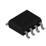
| 描述 | IC COMPARATOR DUAL DIFF 8-SOP模拟比较器 Dual Comparator |
| 产品分类 | |
| 品牌 | Fairchild Semiconductor |
| 产品手册 | |
| 产品图片 |
|
| rohs | 符合RoHS无铅 / 符合限制有害物质指令(RoHS)规范要求 |
| 产品系列 | 校验器 IC,Fairchild Semiconductor KA393DTF- |
| 数据手册 | |
| 产品型号 | KA393DTF |
| 产品种类 | 模拟比较器 |
| 传播延迟(最大值) | - |
| 供应商器件封装 | 8-SOP |
| 偏转电压—最大值 | 9 mV |
| 元件数 | 2 |
| 其它名称 | KA393DTFCT |
| 包装 | 剪切带 (CT) |
| 单位重量 | 143 mg |
| 响应时间 | 1.4 us |
| 商标 | Fairchild Semiconductor |
| 安装类型 | 表面贴装 |
| 安装风格 | SMD/SMT |
| 封装 | Reel |
| 封装/外壳 | 8-SOIC(0.154",3.90mm 宽) |
| 封装/箱体 | SOP-8 |
| 工作温度 | 0°C ~ 70°C |
| 工厂包装数量 | 3000 |
| 最大功率耗散 | 570 mW |
| 最大工作温度 | + 70 C |
| 最小工作温度 | 0 C |
| 标准包装 | 1 |
| 滞后 | - |
| 电压-电源,单/双 (±) | 2 V ~ 36 V, ±1 V ~ 18 V |
| 电压-输入失调(最大值) | 5mV @ 5V |
| 电压增益dB | 106.02 dB |
| 电流-输入偏置(最大值) | 0.25µA @ 5V |
| 电流-输出(典型值) | 18mA @ 5V |
| 电流-静态(最大值) | 2.5mA |
| 电源电压-最大 | 36 V |
| 电源电压-最小 | 18 V |
| 电源电流 | 1 mA |
| 电源电流—最大值 | 1 mA |
| 类型 | 通用 |
| 系列 | KA393 |
| 输入偏压电流—最大 | 250 nA |
| 输出电流—典型值 | 18 mA |
| 输出类型 | Open Collector |
| 通道数量 | 2 Channel |


- 商务部:美国ITC正式对集成电路等产品启动337调查
- 曝三星4nm工艺存在良率问题 高通将骁龙8 Gen1或转产台积电
- 太阳诱电将投资9.5亿元在常州建新厂生产MLCC 预计2023年完工
- 英特尔发布欧洲新工厂建设计划 深化IDM 2.0 战略
- 台积电先进制程称霸业界 有大客户加持明年业绩稳了
- 达到5530亿美元!SIA预计今年全球半导体销售额将创下新高
- 英特尔拟将自动驾驶子公司Mobileye上市 估值或超500亿美元
- 三星加码芯片和SET,合并消费电子和移动部门,撤换高东真等 CEO
- 三星电子宣布重大人事变动 还合并消费电子和移动部门
- 海关总署:前11个月进口集成电路产品价值2.52万亿元 增长14.8%


PDF Datasheet 数据手册内容提取
Is Now Part of To learn more about ON Semiconductor, please visit our website at www.onsemi.com Please note: As part of the Fairchild Semiconductor integration, some of the Fairchild orderable part numbers will need to change in order to meet ON Semiconductor’s system requirements. Since the ON Semiconductor product management systems do not have the ability to manage part nomenclature that utilizes an underscore (_), the underscore (_) in the Fairchild part numbers will be changed to a dash (-). This document may contain device numbers with an underscore (_). Please check the ON Semiconductor website to verify the updated device numbers. The most current and up-to-date ordering information can be found at www.onsemi.com. Please email any questions regarding the system integration to Fairchild_questions@onsemi.com. ON Semiconductor and the ON Semiconductor logo are trademarks of Semiconductor Components Industries, LLC dba ON Semiconductor or its subsidiaries in the United States and/or other countries. ON Semiconductor owns the rights to a number of patents, trademarks, copyrights, trade secrets, and other intellectual property. A listing of ON Semiconductor’s product/patent coverage may be accessed at www.onsemi.com/site/pdf/Patent-Marking.pdf. ON Semiconductor reserves the right to make changes without further notice to any products herein. ON Semiconductor makes no warranty, representation or guarantee regarding the suitability of its products for any particular purpose, nor does ON Semiconductor assume any liability arising out of the application or use of any product or circuit, and specifically disclaims any and all liability, including without limitation special, consequential or incidental damages. Buyer is responsible for its products and applications using ON Semiconductor products, including compliance with all laws, regulations and safety requirements or standards, regardless of any support or applications information provided by ON Semiconductor. “Typical” parameters which may be provided in ON Semiconductor data sheets and/or specifications can and do vary in different applications and actual performance may vary over time. All operating parameters, including “Typicals” must be validated for each customer application by customer’s technical experts. ON Semiconductor does not convey any license under its patent rights nor the rights of others. ON Semiconductor products are not designed, intended, or authorized for use as a critical component in life support systems or any FDA Class 3 medical devices or medical devices with a same or similar classification in a foreign jurisdiction or any devices intended for implantation in the human body. Should Buyer purchase or use ON Semiconductor products for any such unintended or unauthorized application, Buyer shall indemnify and hold ON Semiconductor and its officers, employees, subsidiaries, affiliates, and distributors harmless against all claims, costs, damages, and expenses, and reasonable attorney fees arising out of, directly or indirectly, any claim of personal injury or death associated with such unintended or unauthorized use, even if such claim alleges that ON Semiconductor was negligent regarding the design or manufacture of the part. ON Semiconductor is an Equal Opportunity/Affirmative Action Employer. This literature is subject to all applicable copyright laws and is not for resale in any manner.
K A 3 9 3 June 2011 / K A 3 9 3 A KA393 / KA393A, KA2903 , K A Dual Differential Comparator 2 9 0 3 — Features Description D u Single Supply Operation: 2V to 36V The KA393 / KA393A / KA2903 series consists of two a independent voltage comparators designed to operate l Dual Supply Operation: ±1V to ±18V from a single power supply over a wide voltage range. D i f Allow Comparison of Voltages Near Ground fe Potential re n Low Current Drain: 800µA Typical t i a Compatible with all Forms of Logic Figure 1. DIPPackage Figure 2. SOICPackage l C Low Input Bias Current: 25nA Typical o m Low Input Offset Current: ±5nA Typical p a Low Offset Voltage: ±1mV Typical r a to r Figure 3. Block Diagram Figure 4. Schematic Ordering Information Part Number Operating Temperature Range Package Packing Method KA393 0 to 70°C Tube 8-Lead DIP KA393A 0 to 70°C Tube KA393DTF 0 to 70°C Tape and Reel KA393ADTF 0 to 70°C 8-Lead SOIC Tape and Reel KA2903DTF -40 to 85°C Tape and Reel © 2001 Fairchild Semiconductor Corporation www.fairchildsemi.com KA393 / KA2903 • Rev. 1.0.3
K A Absolute Maximum Ratings 3 9 Stresses exceeding the absolute maximum ratings may damage the device. The device may not function or be 3 operable above the recommended operating conditions and stressing the parts to these levels is not recommended. / K In addition, extended exposure to stresses above the recommended operating conditions may affect device reliability. A The absolute maximum ratings are stress ratings only. 3 9 3 Symbol Parameter Min. Max. Unit A , V Power Supply Voltage ±18 36 V K CC A VI(DIFF) Differential Input Voltage 36 V 2 9 VI Input Voltage -0.3 +36.0 V 0 3 Output Short Circuit to GND Continuous — Power Dissipation, 8-DIP 1040 D P mW D TA = 25°C 8-SOIC 480 u a l KA393 / KA393A 0 +70 D T Operating Temperature °C OPR i KA2903 -40 +85 f f e T Storage Temperature -65 +150 °C r STG e n Thermal Resistance, 8-DIP 120 t RΘ °C/W i JA Junction-to-Ambient 8-SOIC 260 al C Electrostatic Discharge Human Body Model, JESD22-A114 1000 o ESD V Capability Charged Device Model, JESD22-C101 2000 m p a r a t o r © 2001 Fairchild Semiconductor Corporation www.fairchildsemi.com KA393 / KA2903 • Rev. 1.0.3 2
K A Electrical Characteristics 3 9 VCC = 5V and TA = 25°C, Unless otherwise specified. 3 / Symbol Parameter Conditions Min. Typ. Max. Unit K A VO(P) =1.4V, RS =0Ω ±1 ±5 3 KA393 9 Input Offset VCM= 0 to1.5V, TA= 0 to +70°C ±9 3 VIO Voltage KA393A VO(P) =1.4V, RS =0Ω ±1 ±2 mV A, K V = 0 to1.5V, T = 0 to +70°C ±4 CM A A T =25°C ±5 ±50 2 I Input Offset Current A nA 9 IO T = 0 to +70°C ±150 0 A 3 T =25°C 65 250 — A I Input Bias Current nA BIAS TA= 0 to +70°C 400 D u Input Common-Mode Voltage TA=25°C 0 VCC-1.5 a VI(R) Range TA= 0 to +70°C 0 VCC-2.0 V l D i R = ∞, V = 5V 0.6 1.0 f L CC f ICC Supply Current mA e R = ∞, V = 30V 0.8 2.5 r L CC e V =15V, R ≥15KΩ, n V Voltage Gain CC L 50 200 V/mV t G (for Large VO(P-P) Swing) ia l t Large Signal Response Time VI =TTL Logic Swing VREF =1.4V, 350 ns C LRES V =5V, R =5.1KΩ o RL L m tRES Response Time VRL =5V, RL =5.1KΩ 1.4 µs p a ISINK Output Sink Current VI(-) ≥ 1V, VI(+) = 0V, VO(P) ≤ 1.5V 6 18 mA r a V ≥ 1V, V =0V 160 400 t I(-) I(+) o V Output Saturation Voltage mV SAT r ISINK=4mA, TA= 0 to +70°C 700 V = 0V, V = 1V, V = 5V 0.1 nA I(-) I(+) O(P) I Output Leakage Current O(LKG) V = 0V, V = 1V, V = 30V 1.0 µA I(-) I(+) O(P) KA2903 V =1.4V, R =0Ω ±1 ±7 O(P) S V Input Offset Voltage mV IO V = 0 to1.5V, T = -40 to +85°C ±9 ±15 CM A T =25°C ±5 ±50 A I Input Offset Current nA IO T = -40 to +85°C ±50 ±200 A T =25°C 65 250 A I Input Bias Current nA BIAS T = -40 to +85°C 500 A Input Common-Mode Voltage TA=25°C 0 VCC-1.5 V V I(R) Range T = -40 to +85°C 0 V -2.0 A CC R = ∞, V = 5V 0.6 1.0 L CC I Supply Current mA CC R = ∞, V = 30V 1.0 2.5 L CC V =15V, R ≥15KΩ, V Voltage Gain CC L 25 100 V/mV G (for Large V Swing) O(P-P) V =TTL Logic Swing V =1.4V, t Large Signal Response Time I REF 350 ns LRES V =5V, R =5.1KΩ RL L t Response Time V =5V, R =5.1KΩ 1.5 µs RES RL L I Output Sink Current V ≥ 1V, V = 0V, V ≤ 1.5V 6 16 mA SINK I(-) I(+) O(P) V ≥ 1V, V =0V 160 400 I(-) I(+) V Output Saturation Voltage mV SAT I =4mA, T = -40 to +85°C 700 SINK A V = 0V, V = 1V, V = 5V 0.1 nA I(-) I(+) O(P) I Output Leakage Current O(LKG) V = 0V, V = 1V, V = 30V 1.0 µA I(-) I(+) O(P) © 2001 Fairchild Semiconductor Corporation www.fairchildsemi.com KA393 / KA2903 • Rev. 1.0.3 3
K A Typical Performance Characteristics 3 9 3 / K A 3 9 3 A , K A 2 9 0 3 — D u a l D i f Figure 5. Supply Current vs. Supply Voltage Figure 6. Input Current vs. Supply Voltage fe r e n t i a l C o m p a r a t o r Figure 7. Output Saturation Voltage Figure 8. Response Time for Various Input vs. Sink Current Overdrive-Negative Transitions Figure 9. Response Time for Various Input Overdrive-Positive Transitions © 2001 Fairchild Semiconductor Corporation www.fairchildsemi.com KA393 / KA2903 • Rev. 1.0.3 4
K A Physical Dimensions 3 9 3 / K A 5.00 3 4.80 A 0.65 93 A 3.81 , K 8 5 A B 2 9 0 3 6.20 1.75 — 5.80 4.00 5.60 D 3.80 u a l D i f f 1 4 e PIN ONE r e INDICATOR 1.27 n 1.27 ti (0.33) a 0.25 C B A l C LAND PATTERN RECOMMENDATION o 0.25 SEE DETAIL A m p 0.10 a r 0.25 a t o 1.75 MAX C 0.19 r 0.51 0.10 C 0.33 OPTION A - BEVEL EDGE 0.50 x 45° 0.25 R0.10 GAGE PLANE R0.10 OPTION B - NO BEVEL EDGE 0.36 8° NOTES: UNLESS OTHERWISE SPECIFIED 0° A) THIS PACKAGE CONFORMS TO JEDEC MS-012, VARIATION AA, ISSUE C, 0.90 SEATING PLANE B) ALL DIMENSIONS ARE IN MILLIMETERS. 0.40 C) DIMENSIONS DO NOT INCLUDE MOLD FLASH OR BURRS. (1.04) D) LANDPATTERN STANDARD: SOIC127P600X175-8M. DETAIL A E) DRAWING FILENAME: M08AREV13 SCALE: 2:1 Figure 10. 8-Lead, Small-Outline Integrated Circuit (SOIC), JEDEC MS-012, .150" Narrow Body Package drawings are provided as a service to customers considering Fairchild components. Drawings may change in any manner without notice. Please note the revision and/or date on the drawing and contact a Fairchild Semiconductor representative to verify or obtain the most recent revision. Package specifications do not expand the terms of Fairchild’s worldwide terms and conditions, specifically the warranty therein, which covers Fairchild products. Always visit Fairchild Semiconductor’s online packaging area for the most recent package drawings: http://www.fairchildsemi.com/packaging/. © 2001 Fairchild Semiconductor Corporation www.fairchildsemi.com KA393 / KA2903 • Rev. 1.0.3 5
K A Physical Dimensions 3 9 3 / K A .400[10.15] 3 A .373 9.46 9 3 A .036 [0.9 TYP] , K A (.092) [Ø2.337] 2 9 PIN #1 (.032) [R0.813] 0 .250±.005 [6.35±0.13] 3 PIN #1 — D u B a TOP VIEW TOP VIEW l D OPTION 1 OPTION 2 i f f ..007405 [11..7184] .310±.010 [7.87±0.25] ere .130±.005 [3.3±0.13] n t 7° TYP .210 MAX i a [5.33] l C 7° TYP o m p a r a C to .015 MIN r .021[0.53] [0.38] .015 0.37 .140[3.55] .300 .125 3.17 [7.62] .001[.025] C .100 .430 MAX [2.54] [10.92] NOTES: .060 MAX [1.52] A. CONFORMS TO JEDEC REGISTRATION MS-001, +.005[ +0.127] VARIATIONS BA .010-.000 0.254-0.000 B. CONTROLING DIMENSIONS ARE IN INCHES REFERENCE DIMENSIONS ARE IN MILLIMETERS C. DOES NOT INCLUDE MOLD FLASH OR PROTRUSIONS. MOLD FLASH OR PROTRUSIONS SHALL NOT EXCEED .010 INCHES OR 0.25MM. D. DOES NOT INCLUDE DAMBAR PROTRUSIONS. DAMBAR PROTRUSIONS SHALL NOT EXCEED .010 INCHES OR 0.25MM. E. DIMENSIONING AND TOLERANCING PER ASME Y14.5M-1994. N08EREVG Figure 1. 8-Lead, DIP, JEDEC MS-001, .300" Wide Package drawings are provided as a service to customers considering Fairchild components. Drawings may change in any manner without notice. Please note the revision and/or date on the drawing and contact a Fairchild Semiconductor representative to verify or obtain the most recent revision. Package specifications do not expand the terms of Fairchild’s worldwide terms and conditions, specifically the warranty therein, which covers Fairchild products. Always visit Fairchild Semiconductor’s online packaging area for the most recent package drawings: http://www.fairchildsemi.com/packaging/. © 2001 Fairchild Semiconductor Corporation www.fairchildsemi.com KA393 / KA2903 • Rev. 1.0.3 6
K A 3 9 3 / K A 3 9 3 A , K A 2 9 0 3 — D u a l D i f f e r e n t i a l C o m p a r a t o r © 2001 Fairchild Semiconductor Corporation www.fairchildsemi.com KA393 / KA2903 • Rev. 1.0.3 7
ON Semiconductor and are trademarks of Semiconductor Components Industries, LLC dba ON Semiconductor or its subsidiaries in the United States and/or other countries. ON Semiconductor owns the rights to a number of patents, trademarks, copyrights, trade secrets, and other intellectual property. A listing of ON Semiconductor’s product/patent coverage may be accessed at www.onsemi.com/site/pdf/Patent−Marking.pdf. ON Semiconductor reserves the right to make changes without further notice to any products herein. ON Semiconductor makes no warranty, representation or guarantee regarding the suitability of its products for any particular purpose, nor does ON Semiconductor assume any liability arising out of the application or use of any product or circuit, and specifically disclaims any and all liability, including without limitation special, consequential or incidental damages. Buyer is responsible for its products and applications using ON Semiconductor products, including compliance with all laws, regulations and safety requirements or standards, regardless of any support or applications information provided by ON Semiconductor. “Typical” parameters which may be provided in ON Semiconductor data sheets and/or specifications can and do vary in different applications and actual performance may vary over time. All operating parameters, including “Typicals” must be validated for each customer application by customer’s technical experts. ON Semiconductor does not convey any license under its patent rights nor the rights of others. ON Semiconductor products are not designed, intended, or authorized for use as a critical component in life support systems or any FDA Class 3 medical devices or medical devices with a same or similar classification in a foreign jurisdiction or any devices intended for implantation in the human body. Should Buyer purchase or use ON Semiconductor products for any such unintended or unauthorized application, Buyer shall indemnify and hold ON Semiconductor and its officers, employees, subsidiaries, affiliates, and distributors harmless against all claims, costs, damages, and expenses, and reasonable attorney fees arising out of, directly or indirectly, any claim of personal injury or death associated with such unintended or unauthorized use, even if such claim alleges that ON Semiconductor was negligent regarding the design or manufacture of the part. ON Semiconductor is an Equal Opportunity/Affirmative Action Employer. This literature is subject to all applicable copyright laws and is not for resale in any manner. PUBLICATION ORDERING INFORMATION LITERATURE FULFILLMENT: N. American Technical Support: 800−282−9855 Toll Free ON Semiconductor Website: www.onsemi.com Literature Distribution Center for ON Semiconductor USA/Canada 19521 E. 32nd Pkwy, Aurora, Colorado 80011 USA Europe, Middle East and Africa Technical Support: Order Literature: http://www.onsemi.com/orderlit Phone: 303−675−2175 or 800−344−3860 Toll Free USA/Canada Phone: 421 33 790 2910 Fax: 303−675−2176 or 800−344−3867 Toll Free USA/Canada Japan Customer Focus Center For additional information, please contact your local Email: orderlit@onsemi.com Phone: 81−3−5817−1050 Sales Representative © Semiconductor Components Industries, LLC www.onsemi.com www.onsemi.com 1
Mouser Electronics Authorized Distributor Click to View Pricing, Inventory, Delivery & Lifecycle Information: O N Semiconductor: KA393DTF KA393