ICGOO在线商城 > 射频/IF 和 RFID > RF 前端(LNA + PA) > AD9865BCPZ
 Datasheet下载
- 型号: AD9865BCPZ
- 制造商: Analog
- 库位|库存: xxxx|xxxx
- 要求:
| 数量阶梯 | 香港交货 | 国内含税 |
| +xxxx | $xxxx | ¥xxxx |
查看当月历史价格
查看今年历史价格
AD9865BCPZ产品简介:
ICGOO电子元器件商城为您提供AD9865BCPZ由Analog设计生产,在icgoo商城现货销售,并且可以通过原厂、代理商等渠道进行代购。 AD9865BCPZ价格参考¥98.06-¥98.06。AnalogAD9865BCPZ封装/规格:RF 前端(LNA + PA), RF Front End HPNA, VDSL 64-LFCSP-VQ (9x9)。您可以下载AD9865BCPZ参考资料、Datasheet数据手册功能说明书,资料中有AD9865BCPZ 详细功能的应用电路图电压和使用方法及教程。
AD9865BCPZ 是 Analog Devices Inc.(ADI)公司生产的一款高性能射频前端芯片,集成了低噪声放大器(LNA)和功率放大器(PA),主要应用于无线通信系统中。

该芯片广泛用于软件定义无线电(SDR)、基站设备、无线基础设施、点对点微波通信、工业测试设备以及军事通信等领域。其高集成度和优良的射频性能使其在需要高性能发射与接收路径的场景中表现出色。

AD9865BCPZ 支持宽频率范围,具备良好的线性度和噪声系数,适合用于多载波、OFDM等复杂调制系统。此外,它也常被用于医疗成像设备中的射频信号处理模块,以及高端无线传感器网络。

总之,AD9865BCPZ适用于对射频性能要求高、集成度需求强的通信及测试设备中。
| 参数 | 数值 |
| 产品目录 | |
| 描述 | IC PROCESSOR FRONT END 64LFCSP模数转换器 - ADC 10B Broadband Modem Mixed Signal FE |
| 产品分类 | RF 前端 (LNA + PA)集成电路 - IC |
| 品牌 | Analog Devices |
| 产品手册 | |
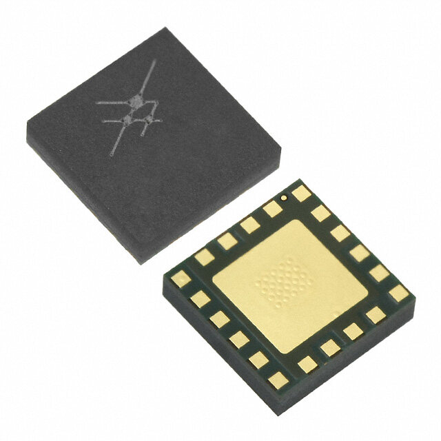
| 产品图片 |
|
| rohs | 符合RoHS无铅 / 符合限制有害物质指令(RoHS)规范要求 |
| 产品系列 | 数据转换器IC,模数转换器 - ADC,Analog Devices AD9865BCPZ- |
| 数据手册 | |
| 产品型号 | AD9865BCPZ |
| RF类型 | HPNA,VDSL |
| 产品种类 | 模数转换器 - ADC |
| 供应商器件封装 | 64-LFCSP-VQ(9x9) |
| 信噪比 | 59 dB |
| 分辨率 | 10 bit |
| 包装 | 托盘 |
| 商标 | Analog Devices |
| 安装风格 | SMD/SMT |
| 封装 | Tray |
| 封装/外壳 | 64-VFQFN 裸露焊盘,CSP |
| 封装/箱体 | LFCSP-64 |
| 工作电源电压 | 3.3 V |
| 工厂包装数量 | 260 |
| 最大功率耗散 | 475 mW |
| 最大工作温度 | + 85 C |
| 最小工作温度 | - 40 C |
| 标准包装 | 1 |
| 特性 | 10 位 ADC,10 位 DAC |
| 电压参考 | Internal |
| 系列 | AD9865 |
| 结构 | Pipeline |
| 视频文件 | http://www.digikey.cn/classic/video.aspx?PlayerID=1364138032001&width=640&height=505&videoID=2245193150001 |
| 转换速率 | 80 MS/s |
| 输入类型 | Differential |
| 通道数量 | 1 Channel |
| 频率 | - |


- 商务部:美国ITC正式对集成电路等产品启动337调查
- 曝三星4nm工艺存在良率问题 高通将骁龙8 Gen1或转产台积电
- 太阳诱电将投资9.5亿元在常州建新厂生产MLCC 预计2023年完工
- 英特尔发布欧洲新工厂建设计划 深化IDM 2.0 战略
- 台积电先进制程称霸业界 有大客户加持明年业绩稳了
- 达到5530亿美元!SIA预计今年全球半导体销售额将创下新高
- 英特尔拟将自动驾驶子公司Mobileye上市 估值或超500亿美元
- 三星加码芯片和SET,合并消费电子和移动部门,撤换高东真等 CEO
- 三星电子宣布重大人事变动 还合并消费电子和移动部门
- 海关总署:前11个月进口集成电路产品价值2.52万亿元 增长14.8%


PDF Datasheet 数据手册内容提取
Broadband Modem Mixed-Signal Front End Data Sheet AD9865 FEATURES FUNCTIONAL BLOCK DIAGRAM Low cost 3.3 V CMOS MxFETM for broadband modems P+ P– 10-bit D/A converter UT_ UT_ O O 2×/4× interpolation filter I I 200 MSPS DAC update rate Integrated 23 dBm line driver with 19.5 dB gain control AD9865 IOUT_G+ 10-bit, 80 MSPS A/D converter PWRMDOWDNE 2-4X TxDAC IAMP IIOOUUTT__NN–+ IOUT_G– −12 dB to +48 dB low noise RxPGA (< 3.0 nV/rtHz) TXEN/SYNC 0 TO–7.5dB 0 TO–12dB TXCLK 10 Third order, programmable low-pass filter CLK CLKOUT_1 Flexible digital data path interface ADIO[9:4]/ SYN. CLKOUT_2 Tx[5:0] Half- and full-duplex operation 2M CLK OSCIN MULTIPLIER XTAL Backward-compatible with AD9975 and AD9875 ADIO[3:0]/ Various power-down/reduction modes Rx[5:0] I2n ateurxnilaial crylo pcrko mgrualmtipmliaebr l(eP cLlLo)c k outputs RXER/SXYCNLKC 10 80AMDSCPS 2-LPPOFLE 1-LPPOFLE RRXX+– Available in 64-lead chip scale package or bare die AGC[5:0] 6 0 TO 6dB – 6 TO 18dB –6 TO 24dB 4 REGISTER ∆ = 1dB ∆ = 6dB ∆ = 6dB SPI CONTROL APoPwPeLrlIiCneA TneIOtwNoSrk ing 04493-0-001 Figure 1. VDSL and HPNA GENERAL DESCRIPTION The AD9865 is a mixed-signal front end (MxFE) IC for or to an internal low distortion current amplifier. The current transceiver applications requiring Tx and Rx path functionality amplifier (IAMP) can be configured as a current- or voltage- with data rates up to 80 MSPS. Its flexible digital interface, mode line driver (with two external npn transistors) capable of power saving modes, and high Tx-to-Rx isolation make it well delivering in excess of 23 dBm peak signal power. Tx power can suited for half- and full-duplex applications. The digital inter- be digitally controlled over a 19.5 dB range in 0.5 dB steps. face is extremely flexible allowing simple interfaces to digital The receive path consists of a programmable amplifier back ends that support half- or full-duplex data transfers, thus (RxPGA), a tunable low-pass filter (LPF), and a 10-bit ADC. often allowing the AD9865 to replace discrete ADC and DAC The low noise RxPGA has a programmable gain range of solutions. Power saving modes include the ability to reduce −12 dB to +48 dB in 1 dB steps. Its input referred noise is less power consumption of individual functional blocks, or to power than 3 nV/rtHz for gain settings beyond 36 dB. The receive path down unused blocks in half-duplex applications. A serial port LPF cutoff frequency can be set over a 15 MHz to 35 MHz interface (SPI®) allows software programming of the various range or simply bypassed. The 10-bit ADC achieves excellent functional blocks. An on-chip PLL clock multiplier and dynamic performance over a 5 MSPS to 80 MSPS span. Both synthesizer provide all the required internal clocks, as well as the RxPGA and the ADC offer scalable power consumption two external clocks from a single crystal or clock source. allowing power/performance optimization. The Tx signal path consists of a bypassable 2×/4× low-pass The AD9865 provides a highly integrated solution for many interpolation filter, a 10-bit TxDAC, and a line driver. The broadband modems. It is available in a space saving 64-pin chip transmit path signal bandwidth can be as high as 34 MHz at an scale package and is specified over the commercial (−40°C to input data rate of 80 MSPS. The TxDAC provides differential +85°C) temperature range. current outputs that can be steered directly to an external load Rev. B Document Feedback Information furnished by Analog Devices is believed to be accurate and reliable. However, no responsibility is assumed by Analog Devices for its use, nor for any infringements of patents or other One Technology Way, P.O. Box 9106, Norwood, MA 02062-9106, U.S.A. rights of third parties that may result from its use. Specifications subject to change without notice. No license is granted by implication or otherwise under any patent or patent rights of Analog Devices. Tel: 781.329.4700 ©2003–2016 Analog Devices, Inc. All rights reserved. Trademarks and registered trademarks are the property of their respective owners. Technical Support www.analog.com
AD9865 Data Sheet TABLE OF CONTENTS Features .............................................................................................. 1 Transmit Path .................................................................................. 28 Applications ....................................................................................... 1 Digital Interpolation Filters ...................................................... 28 Functional Block Diagram .............................................................. 1 TxDAC and IAMP Architecture .............................................. 28 General Description ......................................................................... 1 Tx Programmable Gain Control .............................................. 30 Specifications ..................................................................................... 3 TxDAC Output Operation ........................................................ 30 Tx Path Specifications .................................................................. 3 IAMP Current-Mode Operation .............................................. 30 Rx Path Specifications .................................................................. 4 IAMP Voltage-Mode Operation ............................................... 31 Power Supply Specifications........................................................ 5 IAMP Current Consumption Considerations ........................ 32 Digital Specifications ................................................................... 6 Receive Path .................................................................................... 33 Serial Port Timing Specifications ............................................... 7 Rx Programmable Gain Amplifier ........................................... 33 Half-Duplex Data Interface (ADIO Port) Timing Low-Pass Filter ............................................................................ 34 Specifications ................................................................................ 7 Analog-to-Digital Converter (ADC) ....................................... 35 Full-Duplex Data Interface (Tx and Rx Port) Timing AGC Timing Considerations .................................................... 36 Specifications ................................................................................ 8 Clock Synthesizer ........................................................................... 37 Explanation of Test Levels ........................................................... 8 Power Control and Dissipation .................................................... 39 Absolute Maximum Ratings ............................................................ 9 Power-Down ............................................................................... 39 Thermal Resistance ...................................................................... 9 Half-Duplex Power Savings ...................................................... 39 ESD Caution .................................................................................. 9 Power Reduction Options ......................................................... 40 Pin Configuration and Function Descriptions ........................... 10 Power Dissipation....................................................................... 42 Typical Performance Characteristics ........................................... 12 Mode Select upon Power-Up and Reset .................................. 42 Rx Path Typical Performance Characteristics ........................ 12 Analog and Digital Loop-Back Test Modes ............................ 43 TxDAC Path Typical Performance Characteristics ............... 16 PCB Design Considerations .......................................................... 44 IAMP Path Typical Performance Characteristics .................. 18 Component Placement .............................................................. 44 Serial Port ........................................................................................ 19 Power Planes and Decoupling .................................................. 44 Register Map Description .......................................................... 21 Ground Planes ............................................................................ 44 Serial Port Interface (SPI) .......................................................... 21 Signal Routing ............................................................................. 44 Digital Interface .............................................................................. 23 Evaluation Board ............................................................................ 46 Half-Duplex Mode ..................................................................... 23 Outline Dimensions ....................................................................... 47 Full-Duplex Mode ...................................................................... 24 Ordering Guide .......................................................................... 47 RxPGA Control .......................................................................... 25 TxPGA Control .......................................................................... 27 REVISION HISTORY Changes to Specifications Tables ..................................................... 3 9/2016—Rev. A to Rev. B Changes to Serial Table .................................................................. 19 Changed Thermal Characteristics Section to Thermal Changes to Full Duplex Mode section ......................................... 24 Resistance Section ............................................................................ 9 Change to TxDAC and IAMP Architecture section .................. 29 Changes to Thermal Resistance Section ....................................... 9 Change to TxDAC Output Operation section ............................ 30 Added Table 9; Renumbered Sequentially .................................... 9 Insert equation ................................................................................ 37 Changes to Figure 2 and Table 9 ................................................... 10 Change to Figure 84 caption ......................................................... 42 Changes to Ordering Guide .......................................................... 47 11/2003—Revision 0: Initial Version 11/2004—Rev. 0 to Rev. A Rev. B | Page 2 of 48
Data Sheet AD9865 SPECIFICATIONS Tx PATH SPECIFICATIONS AVDD = 3.3 V ± 5%, DVDD = CLKVDD = DRVDD = 3.3 V ± 10%; f = 50 MHz, f = 200 MHz, R = 2.0 kΩ, unless otherwise OSCIN DAC SET noted. Table 1. Parameter Temp Test Level Min Typ Max Unit TxDAC DC CHARACTERISTICS Resolution Full 10 Bits Update Rate Full II 200 MSPS Full-Scale Output Current (IOUTP_FS) Full IV 2 25 mA Gain Error1 25°C I ±2 % FS Offset Error 25°C V 2 µA Voltage Compliance Range Full −1 +1.5 V TxDAC GAIN CONTROL CHARACTERISTICS Minimum Gain 25°C V −7.5 dB Maximum Gain 25°C V 0 dB Gain Step Size 25°C V 0.5 dB Gain Step Accuracy 25°C IV Monotonic Gain Range Error 25°C V ±2 dB TxDAC AC CHARACTERISTICS2 Fundamental 0.5 dBm Signal-to-Noise and Distortion (SINAD) Full IV 62.0 63.1 dBc Signal-to-Noise Ratio (SNR) Full IV 62.5 63.2 dBc Total Harmonic Distortion (THD) Full IV −77.7 −67.0 dBc Spurious-Free Dynamic Range (SFDR) Full IV 67.1 79.3 dBc IAMP DC CHARACTERISTICS IOUTN Full-Scale Current = IOUTN+ + IOUTN− Full IV 2 105 mA IOUTG Full-Scale Current = IOUTG+ + IOUTG− Full IV 2 150 mA AC Voltage Compliance Range Full IV 1 7 V IAMPN AC CHARACTERISTICS3 Fundamental 25°C 13 dBm IOUTN SFDR (Third Harmonic) Full IV 43.3 45.2 dBc IAMP GAIN CONTROL CHARACTERISTICS Minimum Gain 25°C V −19.5 dB Maximum Gain 25°C V 0 dB Gain Step Size 25°C V 0.5 dB Gain Step Accuracy 25°C IV Monotonic dB IOUTN Gain Range Error 25°C V 0.5 dB REFERENCE Internal Reference Voltage4 25°C I 1.23 V Reference Error Full V 0.7 3.4 % Reference Drift Full V 30 ppm/oC Tx DIGITAL FILTER CHARACTERISTICS (2× Interpolation) Latency (Relative to 1/f ) Full V 43 Cycles DAC −0.2 dB Bandwidth Full V 0.2187 f /f OUT DAC −3 dB Bandwidth Full V 0.2405 f /f OUT DAC Stop-Band Rejection (0.289 f to 0.711 f ) Full V 50 dB DAC DAC Rev. B | Page 3 of 48
AD9865 Data Sheet Parameter Temp Test Level Min Typ Max Unit Tx DIGITAL FILTER CHARACTERISTICS (4× Interpolation) Latency (Relative to 1/ F ) Full V 96 Cycles DAC −0.2 dB Bandwidth Full V 0.1095 f /f OUT DAC −3 dB Bandwidth Full V 0.1202 f /f OUT DAC Stop Band Rejection (0.289 f to 0.711 f ) Full V 50 dB OSCIN OSCIN PLL CLK MULTIPLIER OSCIN Frequency Range Full IV 5 80 MHz Internal VCO Frequency Range Full IV 20 200 MHz Duty Cycle Full II 40 60 % OSCIN Impedance 25°C V 100//3 ΜΩ/pF CLKOUT1 Jitter5 25°C III 12 ps rms CLKOUT2 Jitter6 25°C III 6 ps rms CLKOUT1 and CLKOUT2 Duty Cycle7 Full III 45 55 % 1 Gain error and gain temperature coefficients are based on the ADC only (with a fixed 1.23 V external reference and a 1 V p-p differential analog input). 2 TxDAC IOUTFS = 20 mA, differential output with 1:1 transformer with source and load termination of 50 Ω, FOUT = 5 MHz, 4x interpolation. 3 IOUN full-scale current = 80 mA, fOSCIN = 80 MHz, fDAC =160 MHz, 2x interpolation. 4 Use external amplifier to drive additional load. 5 Internal VCO operates at 200 MHz , set to divide-by-1. 6 Because CLKOUT2 is a divided down version of OSCIN, its jitter is typically equal to OSCIN. 7 CLKOUT2 is an inverted replica of OSCIN, if set to divide-by-1. Rx PATH SPECIFICATIONS AVDD = 3.3 V ± 5%, DVDD = CLKVDD = DRVDD = 3.3 V ± 10%; half- or full-duplex operation with CONFIG = 0 default power bias settings, unless otherwise noted. Table 2. Parameter Temp Test Level Min Typ Max Unit Rx INPUT CHARACTERISTICS Input Voltage Span (RxPGA Gain = −10 dB) Full III 6.33 V p-p Input Voltage Span (RxPGA Gain = +48 dB) Full III 8 mV p-p Input Common-Mode Voltage 25°C III 1.3 V Differential Input Impedance 25°C III 400 Ω 4.0 pF Input Bandwidth (with RxLPF Disabled, RxPGA = 0 dB) 25°C III 53 MHz Input Voltage Noise Density (RxPGA Gain = 36 dB, f−3 dBF = 26 MHz) 25°C III 3.0 nV/rtHz Input Voltage Noise Density (RxPGA Gain = 48 dB, f−3 dBF = 26 MHz) 25°C III 2.4 nV/rtHz RxPGA CHARACTERISTICS Minimum Gain 25°C III −12 dB Maximum Gain 25°C III 48 dB Gain Step Size 25°C III 1 dB Gain Step Accuracy 25°C III Monotonic dB Gain Range Error 25°C III 0.5 dB RxLPF CHARACTERISTICS Cutoff Frequency (f−3 dBF ) Range Full III 15 35 MHz Attenuation at 55.2 MHz with f−3 dBF = 21 MHz 25°C III 20 dB Pass-Band Ripple 25°C III ±1 dB Settling Time to 5 dB RxPGA Gain Step @ f = 50 MSPS 25°C III 20 ns ADC Settling Time to 60 dB RxPGA Gain Step @ f = 50 MSPS 25°C III 100 ns ADC ADC DC CHARACTERISTICS Resolution NA NA 10 Bits Conversion Rate Full II 5 80 MSPS Rev. B | Page 4 of 48
Data Sheet AD9865 Parameter Temp Test Level Min Typ Max Unit Rx PATH LATENCY1 Full-Duplex Interface Full V 10.5 Cycles Half-Duplex Interface Full V 10.0 Cycles Rx PATH COMPOSITE AC PERFORMANCE @ f = 50 MSPS2 ADC RxPGA Gain = 48 dB (Full-Scale = 8.0 mV p-p) Signal-to-Noise and Distortion (SNR) 25°C III 43.7 dBc Total Harmonic Distortion (THD) 25°C III −71 dBc RxPGA Gain = 24 dB (Full-Scale =126 mV p-p) Signal-to-Noise (SNR) 25°C III 59 dBc Total Harmonic Distortion (THD) 25°C III −67.2 dBc RxPGA Gain = 0 dB (Full-Scale = 2.0 V p-p) Signal-to-Noise and Distortion (SINAD) Full IV 58 59 dBc Total Harmonic Distortion (THD) Full IV −66 −62.9 dBc Rx PATH COMPOSITE AC PERFORMANCE @ f = 80 MSPS3 ADC RxPGA Gain = 48 dB (Full-Scale = 8.0 mV p-p) Signal-to-Noise (SNR) 25°C III 41.8 dBc Total Harmonic Distortion (THD) 25°C III −67 dBc RxPGA Gain = 24 dB (Full-Scale = 126 mV p-p) Signal-to-Noise (SNR) 25°C III 58.6 dBc Total Harmonic Distortion (THD) 25°C III −62.9 dBc RxPGA Gain = 0 dB (Full-Scale = 2.0 V p-p) Signal-to-Noise (SNR) 25°C II 58.9 59.6 dBc Total Harmonic Distortion (THD) 25°C II −69.7 −59.8 dBc Rx-to-Tx PATH FULL-DUPLEX ISOLATION (1 V p-p, 10 MHz Sine Wave Tx Output) RxPGA Gain = 40 dB IOUTP± Pins to RX± Pins 25°C III 83 dBc IOUTG± Pins to RX± Pins 25°C III 37 dBc RxPGA Gain = 0 dB IOUTP± Pins to RX± Pins 25°C III 123 dBc IOUTG± Pins to RX± Pins 25°C III 77 dBc 1 Includes RxPGA, ADC pipeline, and ADIO bus delay relative to fADC. 2 fIN = 5 MHz, AIN = −1.0 dBFS , LPF cutoff frequency set to 15.5 MHz with Reg. 0x08 = 0x80. 3 fIN = 5 MHz, AIN = −1.0 dBFS , LPF cutoff frequency set to 26 MHz with Reg. 0x08 = 0x80. POWER SUPPLY SPECIFICATIONS AVDD = 3.3 V, DVDD = CLKVDD = DRVDD = 3.3 V; R = 2 kΩ, full-duplex operation with f = 80 MSPS,1 unless otherwise noted. SET DATA Table 3. Parameter Temp Test Level Min Typ Max Unit SUPPLY VOLTAGES AVDD Full V 3.135 3.3 3.465 V CLKVDD Full V 3.0 3.3 3.6 V DVDD Full V 3.0 3.3 3.6 V DRVDD Full V 3.0 3.3 3.6 V IS_TOTAL (Total Supply Current) Full II 406 475 mA POWER CONSUMPTION IAVDD + ICLKVDD (Analog Supply Current) IV 311 342 mA IDVDD + IDRVDD (Digital Supply Current) Full IV 95 133 mA Rev. B | Page 5 of 48
AD9865 Data Sheet Parameter Temp Test Level Min Typ Max Unit POWER CONSUMPTION (Half-Duplex Operation with f = 50 MSPS)2 DATA Tx Mode IAVDD + ICLKVDD 25°C IV 112 130 mA IDVDD + IDRVDD 25°C IV 46 49.5 mA Rx Mode IAVDD + ICLKVDD 25°C IV 225 253 mA IDVDD + IDRVDD 25°C IV 36.5 39 mA POWER CONSUMPTION OF FUNCTIONAL BLOCKS1 (I + I ) AVDD CLKVDD RxPGA and LPF 25°C III 87 mA ADC 25°C III 108 mA TxDAC 25°C III 38 mA IAMP (Programmable) 25°C III 10 120 mA Reference 25°C III 170 mA CLK PLL and Synthesizer 25°C III 107 mA MAXIMUM ALLOWABLE POWER DISSIPATION Full IV 1.66 W STANDBY POWER CONSUMPTION IS_TOTAL (Total Supply Current) Full 13 mA POWER DOWN DELAY (USING PWR_DWN PIN) RxPGA and LPF 25°C III 440 ns ADC 25°C III 12 ns TxDAC 25°C III 20 ns IAMP 25°C III 20 ns CLK PLL and synthesizer 25°C III 27 ns POWER UP DELAY (USING PWR_DWN PIN) RxPGA and LPF 25°C III 7.8 µs ADC 25°C III 88 ns TxDAC 25°C III 13 µs IAMP 25°C III 20 ns CLK PLL and Synthesizer 25°C III 20 µs 1 Default power-up settings for MODE = HIGH and CONFIG = LOW, IOUTP_FS = 20 mA, does not include IAMP’s current consumption, which is application dependent. 2 Default power-up settings for MODE = LOW and CONFIG = LOW. DIGITAL SPECIFICATIONS AVDD = 3.3 V ± 5%, DVDD = CLKVDD = DRVDD = 3.3 V ± 10%; R = 2 kΩ, unless otherwise noted. SET Table 4. Parameter Temp Test Level Min Typ Max Unit CMOS LOGIC INPUTS High Level Input Voltage Full VI DRVDD – 0.7 V Low Level Input Voltage Full VI 0.4 V Input Leakage Current 12 µA Input Capacitance Full VI 3 pF CMOS LOGIC OUTPUTS (C = 5 pF) LOAD High Level Output Voltage (I = 1 mA) Full VI DRVDD – 0.7 V OH Low Level Output Voltage (I = 1 mA) Full VI 0.4 V OH Output Rise/Fall Time (High Strength Mode and C = 15 pF) Full VI 1.5/2.3 ns LOAD Output Rise/Fall Time (Low Strength Mode and C = 15 pF) Full VI 1.9/2.7 ns LOAD Output Rise/Fall Time (High Strength Mode and C = 5 pF) Full VI 0.7/0.7 ns LOAD Output Rise/Fall Time (Low Strength Mode and C = 5 pF) Full VI 1.0/1.0 ns LOAD RESET Minimum Low Pulse Width (Relative to f ) 1 Clock ADC cycles Rev. B | Page 6 of 48
Data Sheet AD9865 SERIAL PORT TIMING SPECIFICATIONS AVDD = 3.3 V ± 5%, DVDD = CLKVDD = DRVDD = 3.3 V ± 10%, unless otherwise noted. Table 5. Parameter Temp Test Level Min Typ Max Unit WRITE OPERATION (See Figure 46) SCLK Clock Rate (f ) Full IV 32 MHz SCLK SCLK Clock High (t ) Full IV 14 ns HI SCLK Clock Low (t ) Full IV 14 ns LOW SDIO to SCLK Setup Time (t ) Full IV 14 ns DS SCLK to SDIO Hold Time (t ) Full IV 0 ns DH SEN to SCLK Setup Time (tS) Full IV 14 ns SCLK to SEN Hold Time (tH) Full IV 0 ns READ OPERATION (See Figure 47 and Figure 48) SCLK Clock Rate (f ) Full IV 32 MHz SCLK SCLK Clock High (t ) Full IV 14 ns HI SCLK Clock Low (t ) Full IV 14 ns LOW SDIO to SCLK Setup Time (t ) Full IV 14 ns DS SCLK to SDIO Hold Time (t ) Full IV 0 ns DH SCLK to SDIO (or SDO) Data Valid Time (t ) Full IV 14 ns DV SEN to SDIO Output Valid to Hi-Z (tEZ) Full IV 2 ns HALF-DUPLEX DATA INTERFACE (ADIO PORT) TIMING SPECIFICATIONS AVDD = 3.3 V ± 5%, DVDD = CLKVDD = DRVDD = 3.3 V ± 10%, unless otherwise noted. Table 6. Parameter Temp Test Level Min Typ Max Unit READ OPERATION1 (See Figure 50) Output Data Rate Full II 5 80 MSPS Three-State Output Enable Time (t ) Full II 3 ns PZL Three-State Output Disable Time (tPLZ) Full II 3 ns Rx Data Valid Time (t ) Full II 1.5 ns VT Rx Data Output Delay (t ) Full II 4 ns OD WRITE OPERATION (See Figure 49) Input Data Rate (1× Interpolation) Full II 20 80 MSPS Input Data Rate (2× Interpolation) Full II 10 80 MSPS Input Data Rate (4× Interpolation) Full II 5 50 MSPS Tx Data Setup Time (t ) Full II 1 ns DS Tx Data Hold Time (t ) Full II 2.5 ns DH Latch Enable Time (t ) Full II 3 ns EN Latch Disable Time (t ) Full II 3 ns DIS 1 CLOAD = 5 pF for digital data outputs. Rev. B | Page 7 of 48
AD9865 Data Sheet FULL-DUPLEX DATA INTERFACE (Tx AND Rx PORT) TIMING SPECIFICATIONS AVDD = 3.3 V ± 5%, DVDD = CLKVDD = DRVDD = 3.3 V ± 10%, unless otherwise noted. Table 7. Parameter Temp Test Level Min Typ Max Unit Tx PATH INTERFACE (See Figure 53) Input Nibble Rate (2× Interpolation) Full II 20 160 MSPS Input Nibble Rate (4× Interpolation) Full II 10 100 MSPS Tx Data Setup Time (t ) Full II 2.5 ns DS Tx Data Hold Time (t ) Full II 1.5 ns DH Rx PATH INTERFACE1 (See Figure 54) Output Nibble Rate Full II 10 160 MSPS Rx Data Valid Time (t ) Full II 3 ns DV Rx Data Hold Time (t ) Full II 0 ns DH 1 CLOAD =5 pF for digital data outputs. EXPLANATION OF TEST LEVELS I 100% production tested. II 100% production tested at 25°C and guaranteed by design and characterization at specified temperatures. III Sample tested only. IV Parameter is guaranteed by design and characterization testing. V Parameter is a typical value only. VI 100% production tested at 25°C and guaranteed by design and characterization for industrial temperature range. Rev. B | Page 8 of 48
Data Sheet AD9865 ABSOLUTE MAXIMUM RATINGS Table 8. Parameter Rating THERMAL RESISTANCE ELECTRICAL Thermal performance is directly linked to printed circuit board AVDD, CLKVDD Voltage 3.9 V maximum (PCB) design and operating environment. Careful attention to DVDD, DRVDD Voltage 3.9 V maximum PCB thermal design is required. RX+, RX−, REFT, REFB −0.3 V to AVDD + 0.3 V The exposed pad (EPAD) must be soldered to the ground plane IOUTP+, IOUTP− −1.5 V to AVDD + 0.3 V for the 64-lead LFCSP. The EPAD provides an electrical, IOUTN+, IOUTN−, IOUTG+, −0.3 V to +7 V IOUTG− thermal, and mechanical connection to the board. OSCIN, XTAL −0.3 V to CLVDD + 0.3 V Junction temperature (T) can be estimated using the following J REFIO, REFADJ −0.3 V to AVDD + 0.3 V equations: Digital Input and Output Voltage −0.3 V to DRVDD + 0.3 V T = T + (Ψ × P), J T JT Digital Output Current 5 mA maximum or ENVIRONMENTAL Operating Temperature Range −40°C to +85°C T = T + (Ψ × P) J B JB (Ambient) where: Maximum Junction Temperature 125°C T is the temperature measured at the top of the package. Lead Temperature (Soldering, 10 s) 150°C T P is the total device power dissipation. Storage Temperature Range −65°C to +150°C T is the temperature measured at the board. (Ambient) B Ψ and Ψ are thermal characteristic parameters obtained with JT JB Stresses at or above those listed under Absolute Maximum θ in still air test conditions. JA Ratings may cause permanent damage to the product. This is a stress rating only; functional operation of the product at these Table 9. Thermal Resistance or any other conditions above those indicated in the operational Package θJA θJC Unit section of this specification is not implied. Operation beyond CP-64-31 23.32 0.7 °C/W the maximum operating conditions for extended periods may affect product reliability. 1 Test condition 1: typical θJA and θJC values are specified for a 4-layer, JESD51-7 high effective thermal conductivity test board for leaded surface-mount packages. θJA is obtained in still air conditions (JESD51-2). Airflow increases heat dissipation, effectively reducing θJA. θJC is obtained with the test case temperature monitored at the bottom of the exposed pad. ESD CAUTION Rev. B | Page 9 of 48
AD9865 Data Sheet PIN CONFIGURATION AND FUNCTION DESCRIPTIONS N DRVDDDRVSSPWR_DWCLKOUT2DVDDDVSSCLKVDDOSCINXTALCLKVSSCONFIGMODEIOUT_P+IOUT_P–IOUT_N+IOUT_G+ 4321098765432109 6666655555555554 ADIO9/Tx[5] 1 48 AVSS ADIO8/Tx[4] 2 47 AVSS ADIO7/Tx[3] 3 46 IOUT_N– ADIO6/Tx[2] 4 45 IOUT_G– ADIO5/Tx[1] 5 44 AVSS ADIO4/Tx[0] 6 43 AVDD ADIO3/Rx[5] 7 AD9865 42 REFIO ADIO2/Rx[4] 8 TOP VIEW 41 REFADJ ADIO1/Rx[3] 9 (Not to Scale) 40 AVDD ADIO0/Rx[2] 10 39 AVSS NC/Rx[1] 11 38 RX+ NC/Rx[0] 12 37 RX– RXEN/RXSYNC 13 36 AVSS TXEN/TXSYNC 14 35 AVDD TXCLK/TXQUIET 15 34 AVSS RXCLK 16 33 REFT 7890123456789012 1112222222222333 DRVDDDRVSSKOUT1SDIOSDOSCLKSENPGA[5]PGA[4]PGA[3]PGA[2]PGA[1]PGA[0]RESETAVSSREFB CL AIN/ G N1 . O TTTHHEEES EEPXAPDO SPERDOPVAIDDE (SEAPAND E)L MEUCSTTR IBCEA LS,O TLHDEERRMEADLT,OA NTDH EM GECRHOAUNNIDC APLL ACNOEN FNOECRT TIOHEN 6T4O-L TEHAED B LOFACRSDP.. 4493-0-002 Figure 2. Pin Configuration Table 10. Pin Function Descriptions Pin No. Mnemonic Mode1 Description 1 ADIO9 HD MSB of ADIO Buffer Tx[5] FD MSB of Tx Nibble Input 2 to 5 ADIO8 to 5 HD Bits 8 to 5 of ADIO Buffer Tx[4 to 1] FD Bits 4 to 1 of Tx Nibble Input 6 ADIO4 HD Bit 4 of ADIO Buffer Tx[0] FD LSB of Tx Nibble Input 7 ADIO3 HD Bit 3 of ADIO Buffer Rx[5] FD MSB of Rx Nibble Output 8, 9 ADIO2, 1 HD Bits 2 to 1 of ADIO Buffer Rx[4, 3] FD Bits 4 to 3 of Rx Nibble Output 10 ADIO0 HD LSB of ADIO Buffer Rx[2] FD Bit 2 of Rx Nibble Output 11 NC HD No Connect Rx[1] FD Bit 1 of Rx Nibble Output 12 NC HD No Connect Rx[0] FD LSB of Rx Nibble Output 13 RXEN HD ADIO Buffer Control Input RXSYNC FD Rx Data Synchronization Output 14 TXEN HD Tx Path Enable Input TXSYNC FD Tx Data Synchronization Input Rev. B | Page 10 of 48
Data Sheet AD9865 Pin No. Mnemonic Mode1 Description 15 TXCLK HD ADIO Sample Clock Input TXQUIET FD Fast TxDAC/IAMP Power-Down 16 RXCLK HD ADIO Request Clock Input FD Rx and Tx Clock Output at 2 x fADC 17, 64 DRVDD Digital Output Driver Supply Input 18, 63 DRVSS Digital Output Driver Supply Return 19 CLKOUT1 fADC/N Clock Output (L = 1, 2, 4, or 8) 20 SDIO Serial Port Data Input/Output 21 SDO Serial Port Data Output 22 SCLK Serial Port Clock Input 23 SEN Serial Port Enable Input 24 GAIN FD Tx Data Port (Tx[5:0]) Mode Select PGA[5] HD or FD MSB of PGA Input Data Port 25 to 29 PGA[4 to 0] HD or FD Bits 4 to 0 of PGA Input Data Port 30 RESET Reset Input (Active Low) 31, 34, 36, 39, 44, 47, 48 AVSS Analog Ground 32, 33 REFB, REFT ADC Reference Decoupling Nodes 35, 40, 43 AVDD Analog Power Supply Input 37, 38 RX−, RX+ Receive Path − and + Analog Inputs 41 REFADJ TxDAC Full-Scale Current Adjust 42 REFIO TxDAC Reference Input/Output 45 IOUT_G− −Tx Amp Current Output_Sink 46 IOUT_N− −Tx Mirror Current Output_Sink 49 IOUT_G+ +Tx Amp Current Output_Sink 50 IOUT_N+ +Tx Mirror Current Output_Sink 51 IOUT_P− −TxDAC Current Output_Source 52 IOUT_P+ +TxDAC Current Output_Source 53 MODE Digital Interface Mode Select Input LOW = HD, HIGH = FD 54 CONFIG Power-Up SPI Register Default Setting Input 55 CLKVSS Clock Oscillator/Synthesizer Supply Return 56 XTAL Crystal Oscillator Inverter Output 57 OSCIN Crystal Oscillator Inverter Input 58 CLKVDD Clock Oscillator/Synthesizer Supply 59 DVSS Digital Supply Return 60 DVDD Digital Supply Input 61 CLKOUT2 f /L Clock Output, (L = 1, 2, or 4) OSCIN 62 PWR_DWN Power-Down Input EPAD Exposed Pad. The exposed pad (EPAD) must be soldered to the ground plane for the 64-lead LFCSP. The EPAD provides an electrical, thermal, and mechanical connection to the board. 1 HD = half-duplex mode; FD = full-duplex mode. Rev. B | Page 11 of 48
AD9865 Data Sheet TYPICAL PERFORMANCE CHARACTERISTICS Rx PATH TYPICAL PERFORMANCE CHARACTERISTICS AVDD = CLKVDD = DVDD = DRVDD = 3.3 V, f = f = 50 MSPS, low-pass filter’s f = 22 MHz, AIN = −1 dBFS, OSCIN ADC −3 dB RIN = 50 Ω, half- or full-duplex interface, default power bias settings. 10 62 10.0 FUND =–1dBFS 1MHz 0 SINAD = 59.1dBFS 5MHz m) ENOB = 9.53 BITS 59 10MHz 9.5 B–10 SNR = 60.2dBFS 15MHz M (d–20 TSHFDDR = =–6–56.42.d9BdBFSc (THIRD HARMONIC) 56 20MHz 9.0 U R RBW = 12.21kHz RED SPECT–––543000 NAD (dBFS) 5503 88..05 NOB (Bits) ER–60 SI E F RE–70 47 7.5 T U P–80 IN–1–0900 04493-0-040 4414 67..50 04493-0-043 0 6.25 12.50 18.75 25.00 –6 0 6 12 18 24 30 36 42 48 FREQUENCY (MHz) RxPGA GAIN (dB) Figure 3. Spectral Plot with 4 k FFT of Input Sinusoid with Figure 6. SINAD/ENOB vs. RxPGA Gain and Frequency RxPGA = 0 dB and PIN = 9 dBm –55 –30 RBW = 12.2kHz 1MHz –40 5MHz m) –60 10MHz B–50 15MHz M (d 20MHz U–60 –65 R D SPECT––8700 D (dBFC)–70 E H RR–90 T E –75 F RE–100 T INPU–––111321000 04493-0-041 ––8850–6 0 6 12 18 24 30 36 42 4804493-0-044 0 5 10 15 20 25 RxPGA GAIN (dB) FREQUENCY (MHz) Figure 4. Spectral Plot with 4 k FFT of 84-Carrier DMT Signal Figure 7. THD vs. RxPGA Gain and Frequency with PAR = 10.2 dB, PIN = −33.7 dBm, and RxPGA = 36 dB 62 –45 66 –50 SINAD @ +25C SINAD @ +85C 63 –56 59 SINAD @–40C –50 60 –62 56 –55 THD @ +25C SINAD (dBFS) 5547 ––7648 THD (dBFS) SINAD (dBFS) 5503 TTHHDD @@ –+4805CC ––6650 THD (dBc) 51 –80 47 –70 4458–21 –18 SSS–IIINNN15AAADDD @@@ 333–...113424V6VV –9 TTTHHHDDD–6 @@@ 333...1344V6VV–3 0––9826 04493-0-042 4414 ––8705 04493-0-045 INPUT AMPLITUDE (dBFS) –6 0 6 12 18 24 30 36 42 48 0dBFS = 2V p-p RxPGA GAIN (dB) Figure 5. SINAD and THD vs. Input Amplitude and Supply Figure 8. SINAD/THD Performance vs. RxPGA Gain (fIN = 8 MHz, LPF f−3 dB = 26 MHz; Rx PGA = 0 dB) and Temperature ( fIN = 5 MHz) Rev. B | Page 12 of 48
Data Sheet AD9865 Rx PATH TYPICAL PERFORMANCE CHARACTERISTICS AVDD = CLKVDD = DVDD = DRVDD = 3.3 V, f = f = 80 MSPS, low-pass filter’s f = 30 MHz, AIN = −1 dBFS, OSCIN ADC −3 dB RIN = 50 Ω, half- or full-duplex interface, default power bias settings. 10 62 10.0 FUND =–1dBFS 5MHz 0 SINAD = 59.3dBFS 10MHz m) ENOB = 9.56 BITS 59 15MHz 9.5 B–10 SNR = 59.8dBFS 20MHz M (d–20 TSHFDDR = =–6–97.01.d3BdBFSc (THIRD HARMONIC) 56 30MHz 9.0 U R RBW = 19.53kHz RED SPECT–––543000 NAD (dBFS) 5503 88..05 NOB (Bits) ER–60 SI E F RE–70 47 7.5 T U P–80 IN–1–0900 04493-0-046 4414 67..50 04493-0-049 0 10 20 30 40 –6 0 6 12 18 24 30 36 42 48 FREQUENCY (MHz) RxPGA GAIN (dB) Figure 9. Spectral Plot with 4k FFT of Input Sinusoid Figure 12. SINAD/ENOB vs. RxPGA Gain and Frequency with RxPGA = 0 dB and PIN = 9 dBm –30 –55 RBW = 19.53kHz –40 m) –60 B–50 d M ( RU–60 –65 T D SPEC––8700 D (dBc)–70 E H RR–90 T FE –75 RE–100 5MHz INPUT –––111321000 04493-0-047 ––8850 11230500MMMMHHHHzzzz 04493-0-050 0 10 20 30 40 –6 0 6 12 18 24 30 36 42 48 FREQUENCY (MHz) RxPGA GAIN (dB) Figure 10. Spectral Plot with 4k FFT of 111-Carrier DMT Signal with Figure 13. THD vs. RxPGA Gain and Frequency PAR = 11 dB, PIN = −33.7 dBm, LPF f−3 dB = 32 MHz, and RxPGA = 36 dB 66 –50 62 –40 SINAD @ 3.14V THD @ 3.14V SINAD @ +25C SINAD @ 3.3V THD @ 3.3V SINAD @ +85C 63 SINAD @ 3.46V THD @ 3.46V –56 59 SINAD @–40C –45 60 –62 56 –50 SINAD (dBFS) 5547 ––7648 THD (dBFS) SINAD (dBFS) 5503 TTTHHHDDD @@@ ++–428055CCC ––6505 THD (dBc) 51 –80 47 –65 4458 ––9826 04493-0-048 4414 ––7750 04493-0-051 –21 –18 –15 –12 –9 –6 –3 0 –6 0 6 12 18 24 30 36 42 48 INPUT AMPLITUDE (dBFS) RxPGA GAIN (dB) 0dBFS = 2V p-p Figure 11. SINAD and THD vs. Input Amplitude and Supply Figure 14. SINAD/THD Performance vs. RxPGA Gain and Temperature (fIN = 8 MHz, LPF f−3 dB = 26 MHz; RxPGA = 0 dB) ( fIN = 10 MHz) Rev. B | Page 13 of 48
AD9865 Data Sheet 61.0 –52 60.0 –20 SNR @ 3.13V 60.5 SNR @ 3.3V –54 59.5 SNR @ 3.47V 60.0 –56 59.0 SNR @ 3.13V –30 SNR @ 3.3V 59.5 –58 58.5 THD @ 3.13V SNR @ 3.46V SNR (dBFS)555988...050 TTHHDD @@ 33..34V7V –––666024 THD (dBc) SNR (dBFS)555778...050 TTHHDD @@ 33..133VV ––5400 THD (dBc) THD @ 3.46V 57.5 –66 56.5 57.0 –68 56.0 –60 5566..50 ––7702 04493-0-052 5555..05 –70 04493-0-055 –6 0 6 12 18 24 30 36 42 48 20 30 40 50 60 70 80 INPUT FREQUENCY (MHz) INPUT FREQUENCY (MHz) Figure 15. SNR and THD vs. Input Frequency and Supply Figure 18. SNR and THD vs. Sample Rate and Supply ( LPF f−3 dB = 26 MHz; RxPGA = 0 dB) (LPF Disabled; RxPGA = 0 dB; fIN = 8 MHz) 109.4 20 45 98.5 18 z) 44 H OISE (V rms)876765...566 AAADDD999888666555::: –++428055CCC 111642 DENSITY (nV/ dBc)4432 ATED N5443..78 180 CTRAL SNR (41 R E EG32.8 6 SP 40 INT21.9 4 OISE 10.90 20 N04493-0-053 3398 04493-0-056 –6 0 6 12 18 24 30 36 42 48 0 10 20 30 40 50 60 70 80 RxPGA GAIN (dB) CUTOFF FREQUENCY (MHz) Figure 16. Input Referred Integrated Noise and Noise Spectral Density vs. Figure 19. SNR vs. Filter Cutoff Frequency RxPGA Gain (LPF f−3 dB = 26 MHz) (50 MSPS; fIN = 5 MHz; AIN = −1 dB; RxPGA = 48 dB) 5 0.5 4 0.4 3 0.3 e) SET (% of full-scal – 0112 STEP ERROR (dB)–000...1012 FF N C O –2 GAI–0.2 D DEVICE 1 –3 DEVICE 2 –0.3 ––54 DDEEVVIICCEE 34 04493-0-054 ––00..54 AAADDD999888666555::: GGGAAAIIINNN SSSTTTEEEPPP EEERRRRRROOORRR @@@ ++–428055CCC 04493-0-057 –6 0 6 12 18 24 30 36 42 48 –6 0 6 12 18 24 30 36 42 48 GAIN (dB) RxPGA GAIN (dB) Figure 17. Rx DC Offset vs. RxPGA Gain Figure 20. RxPGA Gain Step Error vs. Gain (fIN = 10 MHz) Rev. B | Page 14 of 48
Data Sheet AD9865 Rx PATH TYPICAL PERFORMANCE CHARACTERISTICS AVDD = CLKVDD = DVDD = DRVDD = 3.3 V, f = f = 50 MSPS, low-pass filter disabled, RxPGA = 0 dB, AIN = −1 dBFS, OSCIN ADC RIN = 50 Ω, half- or full-duplex interface, default power bias settings. 512 352 320 448 288 384 256 E 320 E 224 D D O O C 256 C 192 160 192 128 16248 04493-0-058 9664 04493-0-061 0 80 160 240 320 400 480 560 640 720 0 80 160 240 320 400 480 560 640 720 TIME (ns) TIME (ns) Figure 21. RxPGA Settling Time −12 dB to +48 dB Transition for DC Input Figure 24. RxPGA Settling Time for 0 dB to +5 dB Transition for DC Input (fADC = 50 MSPS, LPF Disabled) (fADC = 50 MSPS, LPF Disabled) 0 0 3.3V –6dB GAIN 3.0V –2 0dB GAIN 3.6V +6dB GAIN –3 –4 B) d SE ( –6 dB) –6 ON L ( –8 P A RES –9 ENT –10 PLITUDE –12 FUNDAM ––1142 +++134802dddBBB GGGAAAIIINNN M A –16 –15 –18 04493-0-059 ––2108 04493-0-062 0 5 10 15 20 25 30 35 40 45 50 0 5 10 15 20 25 30 35 40 45 50 INPUT FREQUENCY (MHz) INPUT FREQUENCY (MHz) Figure 22. Rx Low-Pass Filter Amplitude Response vs. Supply Figure 25. Rx Low-Pass Filter Amplitude Response vs. RxPGA Gain (fADC = 50 MSPS, f−3 dB = 33 MHz, RxPGA = 0 dB) (LPF's f−3 dB = 33 MHz) 140 420 10 410 9 130 TxDAC ISOLATION @ 0dB 400 8 B) 120 N (d@RxPGA = 0dB11901000 ESISTANCE ()333367890000 RIN 4567 PACITANCE (pF) TTE R350 CIN 3 CA A 80 IAMP ISOLATION @ 0dB 340 2 6700 04493-0-060 332300 01 04493-0-090 0 5 10 15 20 25 30 35 5 15 25 35 45 55 65 75 85 95 105 FREQUENCY (MHz) FREQUENCY (MHz) Figure 23. Rx to Tx Full-Duplex Isolation @ 0 RxPGA Setting Figure 26. Rx Input Impedance vs. Frequency (Note: ATTEN @ RxPGA = x dB = ATTEN @ RxPGA = 0 dB − RxPGA Gain) Rev. B | Page 15 of 48
AD9865 Data Sheet TxDAC PATH TYPICAL PERFORMANCE CHARACTERISTICS AVDD = CLKVDD = DVDD = DRVDD = 3.3 V, f = 50 MSPS and 80 MSPS, RSET = 1.96 kΩ, 2:1 transformer coupled output OSCIN (see Figure 63) into 50 Ω load half- or full-duplex interface, default power bias settings. 10 10 0 0 –10 –10 –20 –20 –30 –30 m m B B d –40 d –40 –50 –50 –60 –60 ––8700 04493-0-072 ––8700 04493-0-075 0 5 10 15 20 30 0 5 10 15 20 25 30 35 40 FREQUENCY (MHz) FREQUENCY (MHz) Figure 27. Dual-Tone Spectral Plot of TxDAC's Output Figure 30. Dual-Tone Spectral Plot of TxDAC's Output (fDATA = 50 MSPS, 4× Interpolation, 10 dBm Peak Power, (fDATA = 80 MSPS, 2× Interpolation, 10 dBm Peak Power, F1 = 17 MHz, F2 = 18 MHz) F1 = 27.1 MHz, F2 = 28.7 MHz) –65 –65 –70 –70 R) R) 10dBm E E W W O O S)K P–75 S)K P–75 BFEA 4dBm BFEA 4dBm IMD (dTIVE TO P–80 7dBm IMD (dTIVE TO P–80 7dBm A A L L E E R R ( 10dBm ( –85 –85 –90 04493-0-073 –90 04493-0-076 0 2.5 5.0 7.5 10.0 12.5 15.0 17.5 20.0 0 5 10 15 20 25 30 2-TONE CENTER FREQUENCY (MHz) 2-TONE CENTER FREQUENCY (MHz) Figure 28. 2-Tone IMD Frequency Sweep vs. Peak Power Figure 31. 2-Tone IMD Frequency Sweep vs. Peak Power with fDATA = 50 MSPS, 4× Interpolation with fDATA = 80 MSPS, 2× Interpolation –65 –65 –70 –70 R) R) WE WE 10dBm O O SFDR (dBFS)TIVE TO PEAK P––8705 10dBm 7dBm 4dBm SFDR (dBFS)TIVE TO PEAK P––8705 4dBm A A L L E E (R (R 7dBm –85 –85 –90 04493-0-074 –90 04493-0-077 0 2.5 5.0 7.5 10.0 12.5 15.0 17.5 20.0 0 5 10 15 20 25 30 2-TONE CENTER FREQUENCY (MHz) 2-TONE CENTER FREQUENCY (MHz) Figure 29. 2-Tone Worst Spur Frequency Sweep vs. Peak Power Figure 32. 2-Tone Worst Spur Frequency Sweep vs. Peak Power with fDATA = 50 MSPS, 4× Interpolation with fDATA = 80 MSPS, 2× Interpolation Rev. B | Page 16 of 48
Data Sheet AD9865 –20 –20 PAR = 11.4 PAR = 11.4 RMS =–1.4dBm RMS =–1.4dBm –30 –30 –40 –40 –50 –50 m m B –60 B –60 d d –70 –70 –80 –80 –1–0900 04493-0-078 –1–0900 04493-0-081 0 5 10 15 20 25 0 5 10 15 20 25 30 35 40 FREQUENCY (MHz) FREQUENCY (MHz) Figure 33. Spectral Plot of 84-Carrier OFDM Test Vector Figure 36. Spectral Plot of 111-Carrier OFDM Test Vector (fDATA = 50 MSPS, 4× Interpolation) (fDATA = 80 MSPS, 2× Interpolation) –20 –20 PAR = 11.4 PAR = 11.4 RMS =–1.4dBm RMS =–1.4dBm –30 –30 –40 –40 –50 –50 m m B –60 B –60 d d –70 –70 –80 –80 –1–0900 04493-0-079 –1–0900 04493-0-082 0 25 50 75 100 125 150 175 200 0 20 40 60 80 100 120 140 160 FREQUENCY (MHz) FREQUENCY (MHz) Figure 34. Wideband Spectral Plot of 88-Subcarrier OFDM Test Vector Figure 37. Wideband Spectral Plot of 111-Carrier OFDM Test Vector (fDATA = 50 MSPS, 4× Interpolation) (fDATA = 80 MSPS, 2× Interpolation) 100 95 2-TONE IMD 95 90 2-TONE IMD ONE IMD (dBFS)O PEAK POWER) 889050 ONE IMD (dBFS)O PEAK POWER) 788505 AND 2-TLATIVE T 7705 AND 2-TLATIVE T 70 R RE SNR R RE SNR N( N( 65 S 65 S 5650 04493-0-080 5650 04493-0-083 –24 –21 –18 –15 –12 –9 –6 –3 0 –24 –21 –18 –15 –12 –9 –6 –3 0 AOUT (dBFS) AOUT (dBFS) Figure 35. SNR and SFDR vs. POUT Figure 38. SNR and SFDR vs. POUT (fOUT = 12.55 MHz, fDATA = 50 MSPS, 4× Interpolation) (fOUT = 20 MHz, fDATA = 80 MSPS, 2× Interpolation) Rev. B | Page 17 of 48
AD9865 Data Sheet IAMP PATH TYPICAL PERFORMANCE CHARACTERISTICS AVDD = CLKVDD = DVDD = DRVDD = 3.3 V, f = 50 MSPS, R = 1.58 kΩ, 1:1 transformer coupled output (see Figure 64 and OSCIN SET Figure 65) into 50 Ω load, half- or full-duplex interface, default power bias settings. 20 48 15 RBW = 2.3kHz 2.5MHz 10 46 5MHz 5 44 0 –5 42 –10 m) dBm–––221505 P3 (dB 4308 10MHz –30 OI 15MHz 20MHz –35 36 –40 34 –45 –––655050 04493-0-084 3302 04493-0-087 0 5 10 15 20 25 3.0 3.5 4.0 4.5 5.0 FREQUENCY (MHz) VCM (V) Figure 39. Dual-Tone Spectral Plot of IAMPN Output Figure 42. IOUTN Third-Order Intercept vs. Common-Mode Voltage (IAMP Settings of I = 12.5 mA, N = 4, G = 0, (IAMP Settings of I = 12.5 mA, N = 4, G = 0, 2:1 2:1 Transformer into 75 Ω Loader, VCM = 4.8 V) Transformer into 75 Ω Load) 0 42 PAR = 11.4 RMS = 10.3dBm –10 40 2.5MHz –20 38 –30 m) dBm–40 P3 (dB 36 5MHz OI –50 10MHz 34 –60 15MHz 32 ––8700 04493-0-085 30 20MHz 04493-0-088 0 5 10 15 20 25 3.0 3.5 4.0 4.5 5.0 FREQUENCY (MHz) VCM (V) Figure 40. Spectral Plot of 84-Carrier OFDM Test Vector Using IAMPN in Figure 43. IOUTG Third-Order Intercept vs. Common-Mode Voltage Current-Mode Configuration (IAMP Settings of I = 4.25 mA, N = 0, G = 6, (IAMP Settings of I = 10 mA, N = 4, G = 0; VCM = 4.8 V) 2:1 Transformer into 75 Ω Load) 0 0 PAR = 11.4 PAR = 11.4 RMS = 10.4dBm RMS = 9.8dBm –10 –10 RBW = 10kHz –20 –20 –30 –30 Bm–40 dBm–40 d –50 –50 –60 –60 ––8700 04493-0-086 ––87000 5 10 15 20 2504493-0-089 0 5 10 15 20 25 FREQUENCY (MHz) FREQUENCY (MHz) Figure 44. Spectral Plot of 84-Carrier OFDM Test Vector Using IAMP in Figure 41. Spectral Plot of 84-Carrier OFDM Test Vector Using IAMP in Voltage-Mode Configuration with AVDD = 3.3 V Voltage-Mode Configuration with AVDD = 5 V (PBR951 Transistors, IAMP Settings of I = 6 mA, N = 2, G = 6) (PBR951 Transistors, IAMP Settings of I = 6 mA, N = 2, G = 6) Rev. B | Page 18 of 48
Data Sheet AD9865 SERIAL PORT Table 11. SPI Register Mapping Power-Up Default Value Bit Address Break- MODE = 0 (Half-Duplex) MODE = 1 (Full-Duplex) (Hex)1 down Description Width CONFIG = 0 CONFIG = 1 CONFIG = 0 CONFIG = 1 Comments SPI PORT CONFIGURATION AND SOFTWARE RESET 0x00 (7) 4-Wire SPI 1 0 0 0 0 Default SPI configuration is (6) LSB First 1 0 0 0 0 3-wire, MSB first. (5) S/W Reset 1 0 0 0 0 POWER CONTROL REGISTERS (via PWR_DWN pin) 0x01 (7) Clock Syn. 1 0 0 0 0 PWR_DWN = 0. (6) TxDAC/IAMP 1 0 0 0 0 Default setting is for all blocks powered on. (5) Tx Digital 1 0 0 0 0 (4) REF 1 0 0 0 0 (3) ADC CML 1 0 0 0 0 (2) ADC 1 0 0 0 0 (1) PGA Bias 1 0 0 0 0 (0) RxPGA 1 0 0 0 0 0x02 (7) CLK Syn. 1 0 0 0 1* PWR_DWN = 1. (6) TxDAC/IAMP 1 1 1 1 1 Default setting* is for all functional blocks powered (5) Tx Digital 1 1 1 1 1 down except PLL. (4) REF 1 1 1 1 1 *MODE = CONFIG = 1. (3) ADC CML 1 1 1 1 1 Setting has PLL powered (2) ADC 1 1 1 1 1 down with OSCIN input routed to RXCLK output. (1) PGA Bias 1 1 1 1 1 (0) RxPGA 1 1 1 1 1 HALF-DUPLEX POWER CONTROL 0x03 (7:3) Tx OFF Delay 5 Default setting is for TXEN (2) Rx _TXEN 1 input to control power 0xFF 0xFF N/A N/A on/off of Tx/Rx path. (1) Tx PWRDN 1 Tx driver delayed by 31 (0) Rx PWRDN 1 1/f clock cycles. DATA PLL CLOCK MULTIPLIER/SYNTHESIZER CONTROL 0x04 (5) Duty Cycle Enable 1 0 0 0 0 Default setting is Duty Cycle (4) fADC from PLL 1 0 0 0 0 Restore disabled, ADC CLK from OSCIN input, and PLL (3:2) PLL Divide-N 2 00 00 00 00 multiplier × 2 setting. (1:0) PLL Multiplier-M 2 01 10* 01 01 *PLL multiplier × 4 setting. 0x05 (2) OSCIN to RXCLK 1 0 0 0 1* Full-duplex RXCLK normally (1) Invert RXCLK 1 0 0 0 0 at nibble rate. *Exception on power-up. (0) Disabled RXCLK 1 0 0 0 0 0x06 (7:6) CLKOUT2 Divide 2 01 01 01 01 Default setting is CLKOUT2 (5) CLKOUT2 Invert 1 0 0 0 0 and CLKOUT1 enabled with divide-by-2. (4) CLKOUT2 Disable 1 0 0 0 1* *CLKOUT1 and CLKOUT2 (3:2) CLKOUT1 Divide 2 01 01 01 01 disabled. (1) CLKOUT1 Invert 1 0 0 0 0 (0) CLKOUT1 Disable 1 0 0 0 1* Rev. B | Page 19 of 48
AD9865 Data Sheet Power-Up Default Value Bit Address Break- MODE = 0 (Half-Duplex) MODE = 1 (Full-Duplex) (Hex)1 down Description Width CONFIG = 0 CONFIG = 1 CONFIG = 0 CONFIG = 1 Comments Rx PATH CONTROL 0x07 (5) Initiate Offset Cal. 1 0 0 0 0 Default setting has LPF ON (4) Rx Low Power 1 0 1* 0 1* and Rx path at nominal power bias setting. (0) Rx Filter ON 1 1 1 1 1 *Rx path to low power. 0x08 (7:0) Rx Filter Tuning 8 Refer to Low-Pass Filter Cut-off Frequency 0x80 0x61 0x80 0x80 section. Tx/Rx PATH GAIN CONTROL 0x09 (6) Use SPI Rx Gain 1 Default setting is for (5:0) Rx Gain Code 6 0x00 0x00 0x00 0x00 hardware Rx gain code via PGA or Tx data port. 0x0A (6) Use SPI Tx Gain 1 Default setting is for Tx gain (5:0) Tx Gain Code 6 0x7F 0x7F 0x7F 0x7F code via SPI control. Tx AND Rx PGA CONTROL 0x0B (6) PGA Code for Tx 1 0 0 0 0 Default setting is RxPGA (5) PGA Code for Rx 1 1 1 1 1 control active. *Tx port with GAIN strobe (3) Force GAIN strobe 1 0 0 0 0 (AD9875/AD9876-compatible). (2) Rx Gain on Tx Port 1 0 0 1* 1* ** 3-bit RxPGA gain map (1) 3-Bit RxPGA Port 1 0 1** 0 0 (AD9975-compatible). Tx DIGITAL FILTER AND INTERFACE 0x0C (7:6) Interpolation 2 01 00 01 01 Default setting is 2× Factor interpolation with LPF (4) Invert 1 0 0 0 0 response. Data format is TXEN/TXSYNC straight binary for half- duplex and twos (3) Tx 5/5 Nibble* 1 N/A N/A 0 0 complement for full-duplex (2) LS Nibble First* 1 N/A N/A 0 0 interface. (1) TXCLK neg. edge 1 0 0 0 0 *Full-duplex only. (0) Twos complement 1 0 0 1 1 Rx INTERFACE AND ANALOG/DIGITAL LOOPBACK 0x0D (7) Analog Loopback 1 0 0 0 0 Data format is straight (6) Digital Loopback* 1 0 0 0 0 binary for half-duplex and twos complement for full- (5) Rx Port 3-State 1 N/A N/A 0 0 duplex interface. (4) Invert 1 0 0 0 0 Analog loopback: ADC Rx RXEN/RXSYNC data fed back to TxDAC. (3) RX 5/5 Nibble 1 N/A N/A 0 0 Digital loopback: Tx input (2) LS Nibble First* 1 N/A N/A 0 0 data to Rx output port. *Full-duplex only. (1) RXCLK neg. edge 1 0 0 0 0 (0) Twos complement 1 0 0 1 1 DIGITAL OUTPUT DRIVE STRENGTH, TxDAC OUTPUT, AND REV ID 0x0E (7) Low Drive 1 0 0 0 0 Default setting is for high Strength drive strength and IAMP (0) TxDAC Output 1 0 0 0 0 enabled. 0x0F (3:0) REV ID Number 4 0x00 0x00 0x00 0x00 Tx IAMP GAIN AND BIAS CONTROL 0x10 (7) Select Tx Gain 1 Secondary path G1 = 0, 1, 2, (6:4) G1 3 0x44 0x44 0x44 0x44 3, 4. Primary path N = 0, 1, 2, 3, 4. (2:0) N 3 Rev. B | Page 20 of 48
Data Sheet AD9865 Power-Up Default Value Bit Address Break- MODE = 0 (Half-Duplex) MODE = 1 (Full-Duplex) (Hex)1 down Description Width CONFIG = 0 CONFIG = 1 CONFIG = 0 CONFIG = 1 Comments 0x11 (6:4) G2 3 Secondary path stages: (2:0) G3 3 0x62 0x62 0x62 0x62 G2 = 0 to 1.50 in 0.25 steps and G3 = 0 to 6. 0x12 (6:4) Stand_Secondary 3 Standing current of primary 0x01 0x01 0x01 0x01 (2:0) Stand_Primary 3 and secondary path. 0x13 (7:5) CPGA Bias Adjust 3 Current bias setting for Rx (4:3) SPGA Bias Adjust 2 0x00 0x00 0x00 0x00 path’s functional blocks. Refer to page 41. (2:0) ADC Bias Adjust 4 1 Bits that are undefined should always be assigned a 0. REGISTER MAP DESCRIPTION Table 12. SPI Registers Pertaining to SPI Options The AD9865 contains a set of programmable registers described Address (Hex) Bit Description in Table 11 that are used to optimize its numerous features, 0x00 (7) Enable 4-wire SPI interface options, and performance parameters from its default (6) Enable SPI LSB first register settings. Registers pertaining to similar functions have A 4-wire SPI can be enabled by setting the 4-wire SPI bit high, been grouped together and assigned adjacent addresses to causing the output data to appear on the SDO pin instead of on minimize the update time when using the multibyte serial port the SDIO pin. The SDIO pin serves as an input-only throughout interface (SPI) read/write feature. Bits that are undefined within the read operation. Note that the SDO pin is active only during a register should be assigned a 0 when writing to that register. the transmission of data and remains three-stated at any other The default register settings were intended to allow some time. applications to operate without the use of an SPI. The AD9865 An 8-bit instruction header must accompany each read and can be configured to support a half- or full-duplex digital write operation. The instruction header is shown in Table 13. interface via the MODE pin, with each interface having two The MSB is an R/W indicator bit with logic high indicating a possible default register settings determined by the setting of read operation. The next two bits, N1 and N0, specify the the CONFIG pin. number of bytes (one to four bytes) to be transferred during the For instance, applications that need to use only the Tx or Rx data transfer cycle. The remaining five bits specify the address path functionality of the AD9865 can configure it for a half- bits to be accessed during the data transfer portion. The data duplex interface (MODE = 0), and use the TXEN pin to select bits immediately follow the instruction header for both read between the Tx or Rx signal path with the unused path and write operations. remaining in a reduced power state. The CONFIG pin can be used to select the default interpolation ratio of the Tx path and Table 13. Instruction Header Information RxPGA gain mapping. MSB LSB 17 16 15 14 13 12 11 10 SERIAL PORT INTERFACE (SPI) R/W N1 N0 A4 A3 A2 A1 A0 The serial port of the AD9865 has 3- or 4-wire SPI capability allowing read/write access to all registers that configure the The AD9865 serial port can support both MSB (most device’s internal parameters. Registers pertaining to the SPI are significant bit) first and LSB (least significant bit) first data listed in Table 12. The default 3-wire serial communication port formats. Figure 45 illustrates how the serial port words are built consists of a clock (SCLK), serial port enable (SEN), and a bi- for the MSB first and LSB first modes. The bit order is con- directional data (SDIO) signal. SEN is an active low control trolled by the SPI LSB first bit (Register 0, Bit 6). The default gating read and write cycle. When SEN is high, SDO and SDIO value is 0, MSB first. Multibyte data transfers in MSB format are three-stated. The inputs to SCLK, SEN, and SDIO contain a can be completed by writing an instruction byte that includes Schmitt trigger with a nominal hysteresis of 0.4 V centered the register address of the last address to be accessed. The about VDDH/2. The SDO pin remains three-stated in a 3-wire AD9865 automatically decrements the address for each succes- SPI interface. sive byte required for the multibyte communication cycle. Rev. B | Page 21 of 48
AD9865 Data Sheet Figure 47 illustrates the timing for a 3-wire read operation to INSTRUCTIONCYCLE DATATRANSFERCYCLE SEN the SPI port. After SEN goes low, data (SDIO) pertaining to the SCLK instruction header is read on the rising edges of SCLK. A read SDATA R/W N1 N2 A4 A3 A2 A1 A0 D71 D61 D1N D0N operation occurs, if the read/not-write indicator is set high. After the address bits of the instruction header are read, the eight data bits pertaining to the specified register are shifted out of the SDIO pin on the falling edges of the next eight clock cycles. INSTRUCTIONCYCLE DATATRANSFERCYCLE SEN If a multibyte communication cycle is specified in the instruction SCLK header, a similar process as previously described for a multibyte SDATA A0 A1 A2 A3 A4 N2 N1 R/W D01D11 D6N D7N SPI write operation applies. The SDO pin remains three-stated 4493-0-003 in a 3-wire read operation. Figure 45. SPI Timing, MSB First (Upper), and LSB First (Lower) tS1/fSCLK SEN When the SPI LSB first bit is set high, the serial port interprets tHI tLOW SCLK bfbeyorttseh i tnihn LasttS riBun ccfotluiromdnea sat n tchdae nd r abetgeai scbtoyemrte apsd lLedtSreBeds fsbi ryos ftw .t hrMietu ifnlitrgis baty nat dei nddsratetrsaus cttrtoai onbnse - SDIO tDS RtD/WH N1 A2 A1 A0 tDVD7 D6 D1 D0 tEZ 4493-0-005 Figure 47. SPI 3-Wire Read Operation Timing accessed. The AD9865 automatically increments the address for each successive byte required for the multibyte communication Figure 48 illustrates the timing for a 4-wire read operation to cycle. the SPI port. The timing is similar to the 3-wire read operation Figure 46 illustrates the timing requirements for a write opera- with the exception that data appears at the SDO pin, while the tion to the SPI port. After the serial port enable (SEN) signal SDIO pin remains high impedance throughout the operation. goes low, data (SDIO) pertaining to the instruction header is The SDO pin is an active output only during the data transfer read on the rising edges of the clock (SCLK). To initiate a write phase and remains three-stated at all other times. operation, the read/not-write bit is set low. After the instruction header is read, the eight data bits pertaining to the specified tS 1/fSCLK register are shifted into the SDIO pin on the rising edge of the SEN tHI tLOW next eight clock cycles. If a multibyte communication cycle is SCLK specified, the destination address is decremented (MSB first) tDS tDH tEZ and shifts in another eight bits of data. This process repeats until SDIO R/W N1 A2 A1 A0 ashlli fttheed binytteos t hspee ScDifIieOd pinin t. hSeE iNn smtruusctt iroenm haiena dloewr (dNu1ri,n Ng 0t hbeit ds)a atare SDO tDVD7 D6 D1 D0 tEZ 4493-0-006 transfer operation, only going high after the last bit is shifted Figure 48. SPI 4-Wire Read Operation Timing into the SDIO pin. SEN tS1/fSCLK tH tHI tLOW SCLK tDS SDIO RtD/WH N1 N0 A0 D7 D6 D1 D0 4493-0-004 Figure 46. SPI Write Operation Timing Rev. B | Page 22 of 48
Data Sheet AD9865 DIGITAL INTERFACE path, if TXEN is high during this interval with TXCLK present. The digital interface port is configurable for half-duplex or full- The ADIO bus becomes three-stated once the RXEN pin returns duplex operation by pin-strapping the MODE pin low or high, low. Figure 50 shows the receive path output timing. respectively. In half-duplex mode, the digital interface port becomes a 10-bit bidirectional bus called the ADIO port. In RXCLK full-duplex mode, the digital interface port is divided into two 6-bit ports called Tx[5:0] and Rx[5:0] for simultaneous Tx and RXEN tPZL tVT tPtLOZD RAxS IoCp earnadti AonDs.9 I8n6 5th iins 6m-boidt e(,o dr a5t-ab iist )t rnainbsbfleersr.e Tdh bee AtwDe9en86 t5h ea lso ADIO[9:0] RX0 RX1 RX2 RX3 4493-0-008 features a flexible digital interface for updating the RxPGA and Figure 50. Receive Data Output Timing Diagram TxPGA gain registers via a 6-bit PGA port or Tx[5:0] port for To add flexibility to the digital interface port, several program- fast updates, or via the SPI port for slower updates. See the ming options are available in the SPI registers. These options RxPGA Control section for more information. are listed in Table 14. The default Tx and Rx data input formats HALF-DUPLEX MODE are straight binary, but can be changed to twos complement. The default TXEN and RXEN settings are active high, but can The half-duplex mode functions as follows when the MODE be set to opposite polarities, thus allowing them to share the pin is tied low. The bidirectional ADIO port is typically shared same control. In this case, the ADIO port can still be placed in burst fashion between the transmit path and receive path. onto a shared bus by disabling its input latch via the control Two control signals, TXEN and RXEN, from a DSP (or digital signal, and disabling the output driver via the SPI register. The ASIC) control the bus direction by enabling the ADIO port’s clock timing can be independently changed on the transmit and input latch and output driver, respectively. Two clock signals are receive paths by selecting either the rising or falling clock edge also used: TXCLK to latch the Tx input data, and RXCLK to as the validating/sampling edge of the clock. Lastly, the output clock the Rx output data. The ADIO port can also be disabled driver’s strength can be reduced for lower data rate applications. by setting TXEN and RXEN low (default setting), thus allowing it to be connected to a shared bus. Table 14. SPI Registers for Half-Duplex Interface Internally, the ADIO port consists of an input latch for the Tx Address (Hex) Bit Description path in parallel with an output latch with three-state outputs for 0x0C (4) Invert TXEN the Rx path. TXEN is used to enable the input latch; RXEN is (1) TXCLK negative edge used to three-state the output latch. A five-sample-deep FIFO is (0) Twos complement used on the Tx and Rx paths to absorb any phase difference be- 0x0D (5) Rx port three-state tween the AD9865’s internal clocks and the externally supplied (4) Invert RXEN clocks (TXCLK, RXCLK). The ADIO bus accepts input data- (1) RXCLK negative edge words into the transmit path when the TXEN pin is high, the (0) Twos complement RXEN pin is low, and a clock is present on the TXCLK pin, as 0x0E (7) Low digital drive strength shown in Figure 49. tDS The half-duplex interface can be configured to act as a slave or a TXCLK master to the digital ASIC. An example of a slave configuration is shown in Figure 51. In this example, the AD9865 accepts all TXEN tEN tDH tDIS the clock and control signals from the digital ASIC. Because the ADIO[9:0] TX0 TX1 TX2 TX3 TX4 sampling clocks for the DAC and ADC are derived internally RXEN 4493-0-007 fbreo mat ethxaec OtlyS CthINe s saimgnea flr, etqhue eTnXcyC aLsK t haen dO RSCXICNL Ksi gsniganl.a Tlsh me ust Figure 49. Transmit Data Input Timing Diagram phase relationships among the TXCLK, RXCLK, and OSCIN signals can be arbitrary. If the digital ASIC cannot provide a low The Tx interpolation filter(s) following the ADIO port can be jitter clock source to OSCIN, use the AD9865 to generate the flushed with zeros, if the clock signal into the TXCLK pin is clock for its DAC and ADC, and to pass the desired clock signal present for 33 clock cycles after TXEN goes low. Note that the to the digital ASIC via CLKOUT1 or CLKOUT2. data on the ADIO bus is irrelevant over this interval. The output from the receive path is driven onto the ADIO bus when the RXEN pin is high, and a clock is present on the RXCLK pin. While the output latch is enabled by RXEN, valid data appears on the bus after a 6-clock-cycle delay due to the internal FIFO delay. Note that Rx data is not latched back into the Tx Rev. B | Page 23 of 48
AD9865 Data Sheet DIGITAL ASIC AD9865 must be used with a full-duplex interface. ADIO 10 TO The AD9865 acts as the master, providing RXCLK as an output [9:0] Tx DIGITAL clock that is used for the timing of both the Tx[5:0] and Rx[5:0] Tx/Rx FILTER Data[9:0] ports. RXCLK always runs at the nibble rate and can be inverted 10 FROM Rx ADC or disabled via an SPI register. Because RXCLK is derived from the clock synthesizer, it remains active, provided that this func- RXEN RXEN tional block remains powered on. A buffered version of the TXEN TXEN DAC_CLK TXCLK signal appearing at OSCIN can also be directed to RXCLK by ADC_CLK RXCLK setting Bit 2 of Register 0x05. This feature allows the AD9865 to CLKOUT OSCIN 4493-0-009 bweh ciloem seprlveitnelgy apso twheer meda sdtoewr. n (including the clock synthesizer) Figure 51. Example of a Half-Duplex Digital Interface The Tx[5:0] port operates in the following manner with the SPI with AD9865 Serving as the Slave register default settings. Two consecutive nibbles of the Tx data Figure 52 shows a half-duplex interface with the AD9865 acting are multiplexed together to form a 10-bit data-word in twos as the master, generating all the required clocks. CLKOUT1 complement format. The clock appearing on the RXCLK pin is provides a clock equal to the bus data rate that is fed to the a buffered version of the internal clock used by the Tx[5:0] ASIC as well as back to the TXCLK and RXCLK inputs. This port’s input latch with a frequency that is always twice the ADC interface has the advantage of reducing the digital ASIC’s pin sample rate (2 × f ). Data from the Tx[5:0] port is read on the ADC count by three. The ASIC needs only to generate a bus control rising edge of this sampling clock, as illustrated in the timing signal that controls the data flow on the bidirectional bus. diagram shown in Figure 53. Note, TXQUIET must remain DIGITAL ASIC AD9865 high for the reconstructed Tx data to appear as an analog signal at the output of the TxDAC or IAMP. ADIO 10 TO Tx/Rx [9:0] TFxIL DTEIGRITAL ttSDUS Data[9:0] 10 FROM RXCLK Rx ADC tDHtHD TXSYNC RXEN BUS_CTR TTXXECNLK Tx[5:0] Tx0LSB Tx1MSB Tx1LSB Tx2MSB TTxx32LLSSBB Tx3MSB 4493-0-011 RXCLK Figure 53. Tx[5:0] Port Full-Duplex Timing Diagram CLKIN CLKOUT1 The TXSYNC signal is used to indicate to which word a nibble OSCIN belongs. While TXSYNC is low, the first nibble of every word is FCORRROY MMSATSATLER CLK 4493-0-010 rseaamde a ws othrde mis oresat dsi gonni ftihcea nfot lnloibwbinleg. TThXeS sYeNcoCn dh ingihb lbelvee ol fa tsh tahte Figure 52. Example of a Half-Duplex Digital Interface least significant nibble. If TXSYNC is low for more than one with AD9865 Serving as the Master clock cycle, the last transmit data is read continuously until FULL-DUPLEX MODE TXSYNC is brought high for the second nibble of a new trans- mit word. This feature can be used to flush the interpolator The full-duplex mode interface is selected when the MODE pin filters with zeros. Note that the GAIN signal must be kept low is tied high. It can be used for full- or half-duplex applications. during a Tx operation. The digital interface port is divided into two 6-bit ports called The Rx[5:0] port operates in the following manner with the SPI Tx[5:0] and Rx[5:0], allowing simultaneous Tx and Rx opera- register default settings. Two consecutive nibbles of the Rx data tions for full-duplex applications. In half-duplex applications, are multiplexed together to form a 10-bit data-word in twos the Tx[5:0] port can also be used to provide a fast update of the complement format. The Rx data is valid on the rising edge of RxPGA (AD9875 backward-compatible) during an Rx opera- RXCLK, as illustrated in the timing diagram shown in Figure 54. tion. This feature is enabled by default and can be used to The RXSYNC signal is used to indicate to which word a nibble reduce the required pin count of the ASIC (refer to RxPGA belongs. While RXSYNC is low, the first nibble of every word is Control section for details). transmitted as the most significant nibble. The second nibble of In either application, Tx and Rx data are transferred between that same word is transmitted on the following RXSYNC high the ASIC and AD9865 in 6-bit (or 5-bit) nibbles at twice the level as the least significant nibble. internal input/output word rates of the Tx interpolation filter and ADC. Note that the TxDAC update rate must not be less than the nibble rate. Therefore, the 2× or 4× interpolation filter Rev. B | Page 24 of 48
Data Sheet AD9865 For the AD9865, the most significant nibble defaults to 6 bits, tDH and the least significant nibble defaults to 4 bits. This can be RXCLK changed so that the least significant nibble and most significant RXSYNC tDv nibble have 5 bits each. To accomplish this, set the 5/5 nibble bit Rx[5:0] Rx0LSB Rx1MSB Rx1LSB Rx2MSB Rx3LSB Rx3MSB 4493-0-012 iann dR eRgxi[s5te:1r ]0. x0C and Register 0x0D and use data pins Tx[5:1] Figure 55 shows a possible digital interface between an ASIC Figure 54. Full-Duplex Rx Port Timing and the AD9865. The AD9865 serves as the master generating To add flexibility to the full-duplex digital interface port, several the required clocks for the ASIC. This interface requires that the programming options are available in the SPI registers. These ASIC reserve 16 pins for the interface, assuming a 6-bit nibble options are listed in Table 15. The timing for the Tx[5:0] and/or width and the use of the Tx port for RxPGA gain control. Note Rx[5:0] ports can be independently changed by selecting either that the ASIC pin allocation can be reduced by 3, if a 5-bit the rising or falling clock edge as the sampling/validating edge nibble width is used and the gain (or gain strobe) of the RxPGA of the clock. Inverting RXCLK (via Bit 1 or Register 0x05) is controlled via the SPI port. affects both the Rx and Tx interface, because they both use AD9865/AD9866 RXCLK. DIGITAL ASIC 6 OPTIONAL TO GAIN RxPGA Table 15. SPI Registers for Full-Duplex Interface Address (Hex) Bit Description Tx[5:0] UX 10/12 TO 0x05 (2) OSCIN to RXCLK Tx Data[5:0] DEM TFxIL DTEIGRITAL (1) Invert RXCLK (0) Disable RXCLK Rx[5:0] 10/12 0x0B (2) Rx gain on Tx port RxData[5:0] MUX FRRxAODMC 0x0C (4) Invert TXSYNC (3) Tx 5/5 nibble RX_SYNC RXSYNC (2) LS nibble first TX_SYNC TXSYNC (1) TXCLK negative edge CLKIN RXCLK (0) Twos complement CLKOUT1 CLKOUT2 0x0D (5) Rx port three-state (4) Invert RXSYNC OSCIN ((32)) RLSx n5/ib5b nleib fbirlset FCORRROY MMSATSATLER CLK 4493-0-013 (1) RXCLK negative edge Figure 55. Example of a Full-Duplex Digital Interface (0) Twos complement with Optional RxPGA Gain Control via Tx[5:0] 0x0E (7) Low drive strength RxPGA CONTROL The AD9865 contains a digital PGA in the Rx path that is used The default Tx and Rx data input formats are twos complement, but can be changed to straight binary. The default TXSYNC and to extend the dynamic range. The RxPGA can be programmed RXSYNC settings can be changed such that the first nibble of over −12 dB to +48 dB with 1 dB resolution using a 6-bit word, the word appears while TXSYNC, RXSYNC, or both are high. and with a 0 dB setting corresponding to a 2 V p-p input signal. Also, the least significant nibble can be selected as the first The 6-bit word is fed into a LUT that is used to distribute the nibble of the word (LS nibble first). The output driver strength desired gain over three amplification stages within the Rx path. can also be reduced for lower data rate applications. Upon power-up, the RxPGA gain register is set to its minimum gain of −12 dB. The RxPGA gain mapping is shown in Figure 56. Table 16 lists the SPI registers pertaining to the RxPGA. Rev. B | Page 25 of 48
AD9865 Data Sheet 48 t SU 42 RXCLK 36 t 30 TxSYNC HD 24 B) Tx[5:0] GAIN GAIN (d 1128 GAIN 4493-0-015 6 Figure 57. Updating RxPGA via Tx[5:0] in Full-Duplex Mode 0 Updating the RxPGA (or TxPGA) via the PGA[5:0] port is an –6 option for both the half-duplex3 and full-duplex interface. The –120 6 6-B12IT DI1G8ITAL2 4WOR3D0-DE3C6IMAL4 2EQU4IV8ALE5N4T 60 66 4493-0-014 aPpGpAea prionrgt caot nitssi sintsp ouft adnir iencptluyt tbou tfhfeer R thxPatG pAas (soers TthxeP 6G-Abi)t gdaaitna register with no gating signal required. Bit 5 or Bit 6 of Figure 56. Digital Gain Mapping of RxPGA Register 0x0B is used to select whether the data updates the RxPGA or TxPGA gain register. In applications that switch Table 16. SPI Registers RxPGA Control between RxPGA and TxPGA gain control via PGA[5:0], be Address careful that the RxPGA (or TxPGA) is not inadvertently loaded (Hex) Bit Description with the wrong data during a transition. In the case of an 0x09 (6) Enable RxPGA update via SPI RxPGA to TxPGA transition, first deselect the RxPGA gain (5:0) RxPGA gain code register, update the PGA[5:0] port with the desired TxPGA gain 0x0B (6) Select TxPGA via PGA[5:0] setting, and then select the TxPGA gain register. (5) Select RxPGA via PGA[5:0] (3) Enable software GAIN strobe – Full-duplex The RxPGA also offers an alternative 3-bit word gain mapping (2) Enable RxPGA update via Tx[5:0] – Full-duplex option4 that provides a −12 dB to +36 dB span in 8 dB increments (1) 3-bit RxPGA gain mapping – Half-duplex as shown in Table 17. The 3-bit word is directed to PGA[5:3] with PGA[5] being the MSB. This feature is backward-compatible with the AD9975 MxFE and allows direct interfacing to the The RxPGA gain register can be updated via the Tx[5:0] port, CX11647 or INT5130 HomePlug 1.0 PHYs. the PGA[5:0] port, or the SPI port. The first two methods allow fast updates of the RxPGA gain register and should be Table 17. PGA Timing for AD9975 Backward-Compatible considered for digital AGC functions requiring a fast closed- Mode loop response. The SPI port allows direct update and readback of the RxPGA gain register via Register 0x09 with an update Digital Gain Setting rate limited to 1.6 MSPS (with SCLK = 32 MHz). Note that Bit 6 PGA[5:3] Decimal Gain (dB) of Register 0x09 must be set for a read or write operation. 000 0 −12 001 1 −12 Updating the RxPGA via the Tx[5:0] port is an option only in 010 2 −4 full-duplex mode1. In this case, a high level on the GAIN pin,2 011 3 4 with TXSYNC low, programs the PGA setting on either the 100 4 12 rising edge or falling edge of RXCLK, as shown in Figure 57. 101 5 20 The GAIN pin must be held high, TXSYNC must be held low, 110 6 28 and GAIN data must be stable for one or more clock cycles to 111 7 36 update the RxPGA gain setting. A low level on the GAIN pin enables data to be fed to the digital 1 Default setting for full-duplex mode (MODE = 1). 2 The GAIN strobe can also be set in software via Reg. 0x0B, Bit 3 for interpolation filter. This interface should be considered when continuous updating. This eliminates the requirement for external GAIN upgrading existing designs from the AD9875/AD9876 MxFE signal, reducing the ASIC pin count by 1. 3 Default setting for half-duplex mode (MODE = 0). products or half-duplex applications trying to minimize an 4 Default setting for MODE = 0 and CONFIG =1. ASIC’s pin count. Rev. B | Page 26 of 48
Data Sheet AD9865 TXPGA CONTROL The TxPGA register can be updated via the PGA[5:0] port or SPI port. The first method should be considered for fast updates The AD9865 also contains a digital PGA in the Tx path distri- of the TxPGA register. Its operation is similar to the description buted between the TxDAC and IAMP. The TxPGA is used to in the RxPGA Control section. The SPI port allows direct up- control the peak current from the TxDAC and IAMP over a date and readback of the TxPGA register via Register 0x0A with 7.5 dB and 19.5 dB span, respectively, with 0.5 dB resolution. an update rate limited to 1.6 MSPS (SCLK = 32 MHz). Bit 6 of A 6-bit word is used to set the TxPGA attenuation according to Register 0x0A must be set for a read or write operation. the mapping shown in Figure 58. The TxDAC gain mapping is applicable only when Bit 0 of Register 0x0E is set, and only the Table 18 lists the SPI registers pertaining to the TxPGA. The four LSBs of the 6-bit gain word are relevant. TxPGA control register default setting is for minimum attenuation (0 dBFS) with the PGA[5:0] port disabled for Tx 0 –1 gain control. –2 –3 –4 S) –5 F –6 dB –7 Table 18. SPI Registers TxPGA Control ON ( ––89 TxDACs IOUTP OUTPUT Address (Hex) Bit Description NUATI––1101 HAS 7.5dB RANGE 0x0A (6) Enable TxPGA update via SPI TE–12 (5:0) TxPGA gain code T–13 A x –14 0x0B (6) Select TxPGA via PGA[5:0] T–15 –16 IAMPs IOUTN AND IOUTG (5) Select RxPGA via PGA[5:0] ––––21110879 OUTPUTS HAS 19.5dB RANGE 04493-0-063 0x0E (0) TxDAC output (IAMP disabled) 0 8 16 24 32 40 48 56 64 6-BIT DIGITAL CODE (Decimal Equivalent) Figure 58. Digital Gain Mapping of TxPGA Rev. B | Page 27 of 48
AD9865 Data Sheet TRANSMIT PATH The AD9865 (or AD9866) transmit path consists of a selectable is also taken into consideration for applications configured for a digital 2×/4× interpolation filter, a 10-bit or 12-bit TxDAC, and half-duplex interface with the half-duplex power-down mode a current-output amplifier (IAMP) as shown in Figure 59. Note enabled. This feature allows the user to set a programmable that the additional two bits of resolution offered by the AD9866 delay that powers down the TxDAC and IAMP only after the result in a 10 dB to 12 dB reduction in the pass-band noise last Tx input sample has propagated through the digital filter. floor. The digital interpolation filter relaxes the Tx analog See the Power Control and Dissipation section for more details. filtering requirements by simultaneously reducing the images 10 2.5 from the DAC reconstruction process while increasing the WIDE BAND 0 2.0 analog filter’s transition band. The digital interpolation filter ccADaoInOnT[ sx1a[1u5l::6sm0]]o/p bteio bny. pa1s0sed, re2s-u4Xlting in loT0xw DTAOeCr–7 d.5IOUT_P+diBgiIOUT_P–tal c0u TIOrArM–e1P2ndtB IIIIOOOOUUUUTTTT____GNNG–+–+ WIDE BAND RESPONSE (dB)–––––––76543210000000 PASS BAND –1.0dB @ 0.441fDATA –––0011110...505...505 PASS BAND RESPONSE (dB) ADIO[11:6]/ Rx[5:0] –80 –2.0 AD9865/AD9866 TXENT/SXYCNLCK 4493-0-017 –900 0.2N5ORM0A.5L0IZED0 F.7R5EQU1E.0N0CY (R1.e2l5ative 1t.o50fDATA1).75 2.0–02.5 4493-0-018 Figure 59. Functional Block Diagram of Tx Path Figure 60. Frequency Response of 2× Interpolation Filter DIGITAL INTERPOLATION FILTERS (Normalized to fDATA) 10 2.5 The input data from the Tx port can be fed into a selectable WIDE BAND 2×/4× interpolation filter or directly into the TxDAC (for a half- 0 2.0 8dvmfcw2oai0×uoaran p er Mxi Sdl,nbi ePma StexreIpPna uropRtSepmenlf;eio silctgt ylhi baaifn)steter.tipi otoeoTmwumrnnht eas0 . ewe x 4xw nii×0omn iC r5ttidhuen0 w r mt riMpenair ottpDphSeluaP,o A tttflSh iCDawo eAta niT ounsoA rpedf,nd atdi ,tn c8 irawtn0tatooe gthMre sit rslf haseS oaeth Preat o i S ptoniwh sprct ee nl2abi rnc d0eipa0n ilbogto iMieTlwotanaant Sbei5ls Pofl0f ienwiSt l M .t 1if fetTr9ihrSlo.th P imeTisenrS rh s peieesu-t t WIDE BAND RESPONSE (dB)–––––––76543210000000 PA–S1S.0 BdABN @D 0.45fDATA –––0011110...505...505 PASS BAND RESPONSE (dB) –80 –2.0 Table 19. Interpolation Factor Set via SPI Register 0x0C B00it s [7:6] I4n terpolation Factor –900 0.N5ORM1A.L0IZED 1F.5REQUE2.N0CY (R2e.5lative t3o.0fDATA3).5 4.0–2.5 4493-0-019 01 2 Figure 61. Frequency Response of 4× Interpolation Filter 10 1 (half-duplex only) (Normalized to fDATA) 11 Do not use TxDAC AND IAMP ARCHITECTURE The Tx path contains a TxDAC with a current amplifier, IAMP. The interpolation filter consists of two cascaded half-band filter The TxDAC reconstructs the output of the interpolation filter stages with each stage providing 2× interpolation. The first and sources a differential current output that can be directed to stage filter consists of 43 taps. The second stage filter, operating an external load or fed into the IAMP for further amplification. at the higher data rate, consists of 11 taps. The normalized The TxDAC’s and IAMPS’s peak current outputs are digitally wideband and pass-band filter responses (relative f ) for the DATA programmable over a 0 to −7.5 dB and 0 to −19.5 dB range, 2× and 4× low-pass interpolation filters are shown in Figure 60 respectively, in 0.5 dB increments. Note that this assumes and Figure 61, respectively. These responses also include the default register settings for Register 0x10 and Register 0x11. inherent sinc(x) from the TxDAC reconstruction process and can be used to estimate any post analog filtering requirements. The pipeline delays of the 2× and 4× filter responses are 21.5 and 24 clock cycles, respectively, relative to f . The filter delay DATA Rev. B | Page 28 of 48
Data Sheet AD9865 Applications demanding the highest spectral performance IAMP contains two sets of current mirrors that are used to and/or lowest power consumption can use the TxDAC output replicate the TxDAC’s current output with a selectable gain. The directly. The TxDAC is capable of delivering a peak signal first set of current mirrors is designated as the primary path, power-up to 10 dBm while maintaining respectable linearity providing a gain factor of N that is programmable from 0 to 4 in performance, as shown in Figure 27 through Figure 38. For steps of 1 via Bits 2:0 of Register 0x10 with a default setting of power-sensitive applications requiring the highest Tx power N = 4. Bit 7 of this register must be set to overwrite the default efficiency, the TxDAC’s full-scale current output can be reduced settings of this register. This differential path exhibits the best to as low as 2 mA, and its load resistors sized to provide a linearity performance (see Figure 42) and is available at the suitable voltage swing that can be amplified by a low-power op- IOUTN+ and IOUTN− pins. The maximum peak current per amp-based driver. output is 100 mA and occurs when the TxDAC’s standing current, I, is set for 12.5 mA (IOUTFS = 25 mA). Most applications requiring higher peak signal powers (up to 23 dBm) should consider using the IAMP. The IAMP can be The second set of current mirrors is designated as the secon- configured as a current source for loads having a well defined dary path providing a gain factor of G that is programmable impedance (50 Ω or 75 Ω systems), or a voltage source (with the from 0 to 36 via Bits 6:4 of Register 0x10 and Bits 6:0 of Register addition of a pair of npn transistors) for poorly defined loads 0x11 with a default setting of G = 12. This differential path is having varying impedance (such as power lines). intended to be used in the voltage mode configuration to bias the external npn transistors, because it exhibits degraded Figure 62 shows the equivalent schematic of the TxDAC and linearity performance (see Figure 43) relative to the primary IAMP. The TxDAC provides a differential current output path. It is capable of sinking up to 180 mA of peak current into appearing at IOUTP+ and IOUTP−. It can be modeled as a either its IOUTG+ or IOUTG− pins. The secondary path differential current source generating a signal-dependent ac actually consists of three gain stages (G1, G2, and G3), which current, when ∆I has a peak current of I along with two dc S are individually programmable as shown in current sources, sourcing a standing current equal to I. The full- scale output current, IOUTFS, is equal to the sum of these standing current sources (IOUTFS = 2 × I). Table 20. While many permutations may exist to provide a fixed ×∆ (I+I) ×∆ (I–I) ×∆ (I+I) ×∆ (I–I) greamina oinf sG r,e tlhatei vlienlye ainridtye ppeenrfdoernmt aonf cthe eo fv aar sioecuosn inddarivyi dpuatahl gain N N G G settings that are possible to achieve a particular overall gain TxDAC N+ N– G+ G– factor. I I UT UT UT UT REFADJ ±∆IS IO IO IO IO Both sets of mirrors sink current, because they originate from REFIO NMOS devices. Therefore, each output pin requires a dc current RSET 0.1µF path to a positive supply. Although the voltage output of each I +∆I IOUTP+ IOFF1 IOFF1 IOFF2 IOFF2 output pin can swing between 0.5 V and 7 V, optimum ac per- formance is typically achieved by limiting the ac voltage swing I–∆I IOUTP– xN xN xG xG with a dc bias voltage set between 4 to 5 V. Lastly, both the standing current, I, and the ac current, ∆I, from the TxDAC are S IAMP 4493-0-020 acmurprelinfite ddr bawy nth fer ogmain t hfaec ptoors i(tNiv ea nsudp Gpl)y w biethin tgh eeq tuoatal lt ost anding Figure 62. Equivalent Schematic of TxDAC and IAMP 2 × (N = G) × I The value of I is determined by the R value at the REFADJ SET Programmable current sources I and I via Register 0x12 OFF1 OFF2 pin along with the Tx path’s digital attenuation setting. With can be used to improve the primary and secondary path 0 dB attenuation, the value of I is mirrors’ linearity performance under certain conditions by I = 16 × (1.23/RSET) (1) increasing their signal-to-standing current ratio. This feature provides a marginal improvement in distortion performance For example, an R value of 1.96 kΩ results in I equal to SET under large signal conditions when the peak ac current of the 10.0 mA with IOUTFS equal to 20.0 mA. Note that the REFIO pin provides a nominal band gap reference voltage of 1.23 V reconstructed waveform frequently approaches the dc standing and should be decoupled to analog ground via a 0.1 µF current within the TxDAC (0 to −1 dBFS sine wave) causing the capacitor. internal mirrors to turn off. However, the improvement in distortion performance diminishes as the crest factor (peak-to- The differential current output of the TxDAC is always con- rms ratio) of the ac signal increases. Most applications can nected to the IOUTP pins, but can be directed to the IAMP by disable these current sources (set to 0 mA via Register 0x12) to clearing Bit 0 of Register 0x0E. As a result, the IOUTP pins reduce the IAMP’s current consumption. must remain completely open, if the IAMP is to be used. The Rev. B | Page 29 of 48
AD9865 Data Sheet Table 20. SPI Registers for TxDAC and IAMP 1:1 Address (Hex) Bit Description RS RL 0x0E (0) TxDAC output 0.1F RSET 0x10 (7) Enable current mirror gain settings (6:4) Stoe c4o wnditahr ∆y p=a 1t h first stage gain of 0 REFIO REFADJ IOUT_P+ IOUT_P– IIOOUUTTNG++ (3) Not used (2:0) Primary path NMOS gain of 0 to 4 TxDAC IAMP with ∆ = 1 0x11 (7) Don’t care 0 TO–7.5dB 0 TO–12dB IOUTN– (6:4) S0e tcoo 1n.d5 awryit hp a∆t h= s0e.2co5n d stage gain of IOUTG– 4493-0-021 (3) Not used Figure 63. TxDAC Output Directly via Center-Tap Transformer (2:0) Secondary path third stage gain of 0 to 5 with ∆ = 1 The TxDAC is capable of delivering up to 10 dBm peak 0x12 (6:4) IOFF2, secondary path standing power to a load, RL. To increase the peak power for a fixed current standing current, one must increase V p-p across IOUTP+ (2:0) IOFF1, primary path standing current and IOUTP− by increasing one or more of the following parameters: R, R (if possible), and/or the turns ratio, N, of S L transformer. For example, the removal of R and the use of S Tx PROGRAMMABLE GAIN CONTROL a 2:1 impedance ratio transformer in the previous example TxPGA functionality is also available to set the peak output results in 10 dBm of peak power capabilities to the load. current from the TxDAC or IAMP. The TxDAC and IAMP are Note that increasing the power output capabilities of the digitally programmable via the PGA[5:0] port or SPI over a 0 dB TxDAC reduces the distortion performance due to the to −7.5 dB and 0 dB to −19.5 dB range, respectively, in 0.5 dB higher voltage swings seen at IOUTP+ and IOUTP−. See increments. Figure 27 through Figure 38 for performance plots on the TxDAC’s ac performance. Optimum distortion The TxPGA can be considered as two cascaded attenuators with performance can typically be achieved by: the TxDAC providing 7.5 dB range in 0.5 dB increments, and the IAMP providing 12 dB range in 6 dB increments. As a Limiting the peak positive VIOUTP+ and VIOUTP− to 0.8 V to avoid onset of TxDAC’s output compression. (TxDAC’s result, the IAMP’s composite 19.5 dB span is valid only if voltage compliance is around 1.2 V.) Register 0x10 remains at its default setting of 0x44. Modifying this register setting corrupts the LUT and results in an invalid Limiting V p-p seen at IOUTP+ and IOUTP− to less gain mapping. than 1.6 V. TxDAC OUTPUT OPERATION Applications demanding higher output voltage swings and power drive capabilities can benefit from using the IAMP. The differential current output of the TxDAC is available at the IOUTP+ and IOUTP− pins and the IAMP should be disabled IAMP CURRENT-MODE OPERATION by setting Bit 0 of Register 0x0E. Any load connected to these The IAMP can be configured for the current-mode operation as pins must be ground referenced to provide a dc path for the shown in Figure 64 for loads remaining relatively constant. In current sources. Figure 63 shows the outputs of the TxDAC this mode, the primary path mirrors should be used to deliver driving a doubly terminated 1:1 transformer with its center-tap the signal-dependent current to the load via a center-tapped tied to ground. The peak-to-peak voltage, V p-p, across R (and L transformer, because it provides the best linearity performance. IOUT+ to IOUT−) is equal to 2 × I × (R//R). With I = 10 mA L S Because the mirrors exhibit a high output impedance, they can and R = R = 50 Ω, V p-p is equal to 0.5 V with 1 dBm of peak L S be easily back-terminated (if required). power being delivered to R and 1 dBm being dissipated in R. L S For peak signal currents (IOUT up to 50 mA), only the PK primary path mirror gain should be used for optimum distortion performance and power efficiency. The primary path’s gain should be set to 4, with the secondary path’s gain stages set to 0 (Register 0x10 = 0x84). The TxDAC’s standing current, I, can be set between 2.5 mA and 12.5 mA with the IOUTP outputs left open. The IOUTN outputs should be connected to the transformer, with the IOUTG (and IOUTP) outputs left open for optimum linearity performance. The Rev. B | Page 30 of 48
Data Sheet AD9865 transformer1 should be specified to handle the dc standing IAMP VOLTAGE-MODE OPERATION current, I , drawn by the IAMP. Also, because I remains BIAS BIAS The voltage-mode configuration is shown in Figure 65. This signal independent, a series resistor (not shown) can be inserted configuration is suited for applications having a poorly defined between AVDD and the transformer’s center-tap to reduce the load that can vary over a considerable range. A low impedance IAMP’s common-mode voltage, V , and reduce the power CM voltage driver can be realized with the addition of two external dissipation on the IC. The V bias should not exceed 5.0 V and CM RF bipolar npn transistors (Phillips PBR951) and resistors. In the power dissipated in the IAMP alone is as follows: this configuration, the current mirrors in the primary path PIAMP = 2 × (N + G) × I × VCM (2) (IOUTN outputs) feed into scaling resistors, R, generating a differential voltage into the bases of the npn transistors. These transistors are configured as source followers with the secon- 0.1µF RSET AVDD dary path current mirrors appearing at IOUTG+ and IOUTG− providing a signal-dependent bias current. Note that the REFIO REFADJ OUT_P+ OUT_P– IIOOUUTTNG++ 0.1µF IBIAS = 2× (N+G)× 1 IOUTP outputs must remain open for proper operation. I I T:1 0.1µF RSET AVDD TxD0A CTO–7.5dB 0 TO–1IA2MdBP IOUTN– IOUTPK RL REFIO REFADJ IOUT_P+ –IOUT_P IIOOUUTTNG++ R R DPHUIALRLLS INP0PS.1N PµBFR951 Figure 64. Current-MIOoUdTeG O–pePIOr_aUOTtUiPoTKPn =K (=N (+IOGU)×T P1K)2× T2× RL 4493-0-022 TxD0A CTO–7.5dB 0 TO–I1A2MdBP IIOOUUTTGN–– IOUTPK AVDRDS0.1µF TO LOAD 4493-0-023 A step-down transformer1 with a turn ratio, T, can be used to Figure 65. Voltage-Mode Operation increase the output power, P_OUT, delivered to the load. This The peak differential voltage signal developed across the npn’s causes the output load, R, to be reflected back to the IAMP’s L bases is as follows: differential output by T2, resulting in a larger differential voltage VOUT = R × (N × I) (4) swing seen at the IAMP’s output. For example, the IAMP can PK deliver 24 dBm of peak power to a 50 Ω load, if a 1.41:1 step- where: down transformer is used. This results in 5 V p-p voltage swings N is the gain setting of the primary mirror. appearing at IOUTN+ and IOUTN− pins. Figure 42 shows how I is the standing current of the TxDAC defined in Equation 1. the third order intercept point, OIP3, of the IAMP varies as a function of common-mode voltage over a 2.5 MHz to 20.0 MHz The common-mode bias voltage seen at IOUTN+ and IOUTN− span with a 2-tone signal having a peak power of approximately is approximately AVDD − VOUT , while the common-mode PK 24 dBm with IOUTPK = 50 mA. voltage seen at IOUTG+ and IOUTG− is approximately the npn’s V drop below this level (AVDD − VOUT − 0.65). In For applications requiring an IOUT exceeding 50 mA, set the BE PK PK the voltage-mode configuration, the total power dissipated secondary’s path to deliver the additional current to the load. within the IAMP is as follows : IOUTG+ and IOUTN+ should be shorted as well as IOUTG− and IOUTN−. If IOUTPK represents the peak current to be PIAMP = 2 × I × {(AVDD − VOUTPK) × N delivered to the load, then the current gain in the secondary + (AVDD − VOUT − 0.65) × G} (5) PK path, G, can be set by the following equation: The emitters of the npn transistors are ac-coupled to the trans- G = IOUTPK/12.5 − 4 (3) former1 via a 0.1 µF blocking capacitor and series resistor of 1 Ω to 2 Ω. Note that protection diodes are not shown for clarity The linearity performance becomes limited by the secondary purposes, but should be considered if interfacing to a power or mirror path’s distortion. phone line. The amount of standing and signal-dependent current used to bias the npn transistors depends on the peak current, IOUT , PK required by the load. If the load is variable, determine the worst case, IOUT , and add 3 mA of margin to ensure that the npn PK transistors remain in the active region during peak load currents. The gain of the secondary path, G, and the TxDAC’s standing current, I, can be set using the following equation: 1 The B6080 and BX6090 transformers from Pulse Engineering are worthy of IOUT + 3 mA = G × I (6) consideration for current and voltage modes. PK Rev. B | Page 31 of 48
AD9865 Data Sheet The voltage output driver exhibits a high output impedance if 100 the bias currents for the npn transistors are removed. This 90 feature is advantageous in half-duplex applications (for 80 example, power lines) in which the Tx output driver must go into a high impedance state while in Rx mode. If the AD9865 is 70 A) configured for the half-duplex mode (MODE = 0), the IAMP, m 60 TxDAC, and interpolation filter are automatically powered (LY IAMPN OUTPUT PP 50 down after a Tx burst (via TXEN), thus placing the Tx driver SU I into a high impedance state while reducing its power 40 TxDACs AVDD consumption. 30 ICAOMNPS ICDUERRRAETNIOT NCSO NSUMPTION 1200 04493-0-064 1 2 3 4 5 6 7 8 9 10 11 12 13 The Tx path’s analog current consumption is an important I (mA) consideration when determining its contribution to the overall Figure 66. Current Consumption of TxDAC and IAMP in Current-Mode on-chip power dissipation. This is especially the case in full- Operation with IOUTN Only (Default IAMP Settings) duplex applications, where the power dissipation can exceed the 150 maximum limit of 1.66 W, if the IAMP’s IOUT is set to high. 140 PK The analog current consumption includes the TxDAC’s analog 130 IOUTG OUTPUT 120 supply (Pin 43) along with the standing current from the IAMP’s 110 outputs. Equation 2 and Equation 5 can be used to calculate the 100 power dissipated in the IAMP for the current and voltage mode mA) 90 configuration. Figure 66 shows the current consumption for the (LY 80 P TxDAC and IAMP as a function of the TxDAC’s standing current, UP 70 S I 60 I, when only the IOUTN outputs are used. Figure 67 shows the 50 current consumption for the TxDAC and IAMP as a function of TxDAC AVDD 40 the TxDAC’s standing current, I, when the IOUTN and IOUTG ogauitnp usetst tainreg su osef dN. B=o 4th a nfidg uGre =s a1r2e. with the default current mirror 123000 IOUTN OUTPUT 04493-0-065 1.0 1.5 2.0 2.5 3.0 3.5 4.0 4.5 5.0 5.5 6.0 6.5 7.0 I (mA) Figure 67. Current Consumption of TxDAC and IAMP in Current-Mode Operation with IOUTN Only (Default IAMP Settings) Rev. B | Page 32 of 48
Data Sheet AD9865 RECEIVE PATH The receive path block diagram for the AD9865 (or AD9866) is To limit the RxPGA’s self-induced input offset, an offset shown in Figure 68. The receive signal path consists of a 3-stage cancellation loop is included. This cancellation loop is auto- RxPGA, a 3-pole programmable LPF, and a 10-bit (or 12-bit) matically performed upon power-up and can also be initiated ADC. Note that the additional two bits of resolution offered by via SPI. During calibration, the RxPGA’s first stage is internally the AD9866 result in a 3 dB to 5 dB lower noise floor depending shorted, and each gain stage set to a high gain setting. A digital on the RxPGA gain setting and LPF cutoff frequency. Also working servo loop slaves a calibration DAC, which forces the Rx input in conjunction with the receive path is an offset correction circuit. offset to be within ±32 LSB for this particular high gain setting. These blocks are discussed in detail in the following sections. Although the offset varies for other gain settings, the offset is Note that the power consumption of the RxPGA can be modified typically limited to ±5% of the ADC’s 2 V input span. Note that via Register 0x13 as discussed in the Power Control and the offset cancellation circuitry is intended to reduce the voltage Dissipation section. offset attributed to only the RxPGA’s input stage, not any dc offsets attributed to an external source. ADIO[11:6]/ The gain of the RxPGA should be set to minimize clipping of Tx[5:0] CLK CLKOUT_1 SYN. CLKOUT_2 the ADC while utilizing most of its dynamic range. The maxi- ADIOR[x1[15::60]]/ MU2LMT CIPLLKIER XOTSACLIN mum peak-to-peak differential voltage that does not result in clipping of the ADC is shown in Figure 69. While the graph 10/12 RXENR/SXYCNLCK 80AMDSCPS SPGA 2-LPPOFLE 1-LPPOFLE RRXX+– suggests that maximum input signal for a gain setting of −12 dB is 8.0 V p-p, the maximum input voltage into the PGA should 0 TO 6dB –6 TO 18dB –6 TO 24dB ∆ = 1dB ∆ = 6dB ∆ = 6dB be limited to less than 6 V p-p to prevent turning on ESD protec- 6 GAIN tion diodes. For applications having higher maximum input PGA[5:0] MAPPING LUT signals, consider adding an external resistive attenuator network. SPORT 4 RCEOGNITSRTOELR AD9865/AD9866 4493-0-024 While the input sensitivity of the Rx path is degraded by the amount of attenuation on a dB-to-dB basis, the low noise Figure 68. Functional Block Diagram of Rx Path characteristics of the RxPGA provide some design margin such RX PROGRAMMABLE GAIN AMPLIFIER that the external line noise remains the dominant source. The RxPGA has a digitally programmable gain range from 8.0000 V) −12 dB to +48 dB with 1 dB resolution via a 6-bit word. Its N (4.0000 A purpose is to extend the dynamic range of the Rx path such that P the input of the ADC is presented with a signal that scales UT S2.0000 P within its fixed 2 V input span. There are multiple ways of K IN1.0000 setting the RxPGA’s gain as discussed in the RxPGA Control EA0.5000 P section, as well as an alternative 3-bit gain mapping having a TO-0.2500 range of −12 dB to +36 dB with 8 dB resolution. EAK-0.1250 P The RxPGA is comprised of two sections: a continuous time E L0.0625 A PGA (CPGA) for course gain and a switched capacitor PGA C (cSaPscGaAde)d f ogra ifnin set aggaeins prerosovliudtiinogn a. Tghaien C rPanGgAe fcroonmsi s−t1s 2o fd tBw too FULL-S000...000311150260 04493-0-031 +42 dB with 6 dB resolution. The first stage features a low noise –12 –6 0 6 12 18 24 30 36 42 48 preamplifier (< 3.0 nV/rtHz), thereby eliminating the need for GAIN (dB) Figure 69. Maximum Peak-to-Peak Input vs. RxPGA Gain Setting an external preamplifier. The SPGA provides a gain range from that Does Not Result in ADC Clipping 0 dB to 6 dB with 1 dB resolution. A look-up table (LUT) is used to select the appropriate gain setting for each stage. The nominal differential input impedance of the RxPGA input appearing at the device RX+ and RX− input pins is 400 Ω//4 pF (±20%) and remains relatively independent of gain setting. The PGA input is self-biased at a 1.3 V common-mode level allowing maximum input voltage swings of ±1.5 V at RX+ and RX−. AC coupling the input signal to this stage via coupling capacitors (0.1 µF) is recommended to ensure that any external dc offset does not get amplified with high RxPGA gain settings, potentially exceeding the ADC input range. Rev. B | Page 33 of 48
AD9865 Data Sheet LOW-PASS FILTER 0.25 1.30 0 1.25 The low-pass filter (LPF) provides a third order response with a NORMALIZED GAIN RESPONSE –0.25 1.20 cutoff frequency that is typically programmable over a 15 MHz –0.50 1.15 AY tpole 3m5 eMntHedz wspitahni.n F tihgue rfeir 6st8 CshPoGwAs gthaaint tshtaeg feir, satn rde atlh pe ocloem isp ilmex- ––10..0705 11..0150 UP DELE (GDT) pCsctuoaatlpnoeat fspcf aiwftriorietr qih saui rniemr natchpyysele sawmer hetew inuleotse e psddrt ae itngsoee trvshv aieinrn ys gae t chtmohenae dn dnin foCferePrmr GethanAlati t zRg eca-dhCi naf nr tsiegtmqaeugse ee tc.nh ocen y- GAIN (dB)––––2111....07520505 0001....89905050 RMALIZED GROTIME RESPONS response. Because absolute resistor and capacitor values are –2.25 0.80 NO NORMALIZED GROUP DELAY process-dependent, a calibration routine lasting less than 100 μs –2.50 0.75 automatically occurs each time the target cutoff frequency –2.75 0.70 rfreegqisuteenr c(yR efrgoismte rd e0vxi0c8e) t ois duepvdicaete. d, ensuring a repeatable cutoff –3.000 0.1 0.2 N0.O3RM0A.L4IZED0. 5FREQ0.U6ENC0Y.7 0.8 0.9 1.00.65 4493-0-026 Figure 71. LPF’s Normalized Pass-Band Gain and Group Delay Responses Although the default setting specifies that the LPF be active, it can also be bypassed providing a nominal f−3 dB of 55 MHz. The −3 dB cut-off frequency, f−3 dB, is programmable by writing Table 21 shows the SPI registers pertaining to the LPF. an 8-bit word, referred to as the target, to Register 0x08. The cutoff frequency is a function of the ADC sample rate, f , and ADC Table 21. SPI Registers for Rx Low-Pass Filter to a lesser extent, the RxPGA gain setting (in dB). Figure 72 Address (Hex) Bit Description shows how the frequency response, f−3 dB, varies as a function of 0x07 (0) Enable Rx LPF the RxPGA gain setting. 0x08 (7:0) Target value 3 –6dB GAIN 0dB GAIN The normalized wideband gain response is shown in Figure 70. 0 +6dB GAIN +18dB GAIN The normalized pass-band gain and group delay responses are +30dB GAIN –3 +42dB GAIN shown in Figure 71. The normalized cutoff frequency, f−3 dB, dB) results in −3 dB attenuation. Also, the actual group delay time AL ( –6 (GDT) response can be calculated given a programmed cutoff NT E frequency using the following equation: AM –9 D N Actual GDT = Normalized GDT/(2.45 × f−3dB) (7) FU–12 5 –15 0 –5 –180 5 10 1IN5PUT2 F0REQ2U5ENC3Y0 (MHz3)5 40 45 50 4493-0-027 –10 Figure 72. Effects of RxPGA Gain on LPF Frequency Response B) (f−3 dB = 32 MHz (@ 0 dB and fADC = 80 MSPS) AIN (d–15 The following formula1 can be used to estimate f−3 dB for a G–20 RxPGA gain setting of 0 dB: f = (128/target) × (f /80) ×(f /30 + 23.83) f (8) –25 −3dB_0dB ADC ADC Figure 73 compares the measured and calculated f using this –30 −3 dB formula. –350 0.5 1.0 FREQ1U.5ENCY 2.0 2.5 3.04493-0-025 1 Etom 8p0i rMicaSlPlyS dweirtihv eadn fRoxrP aG fA−3 =dB 0r adnBg. e of 15 MHz to 35 MHz and fADC of 40 MSPS Figure 70. LPF’s Normalized Wideband Gain Response Rev. B | Page 34 of 48
Data Sheet AD9865 35 ANALOG-TO-DIGITAL CONVERTER (ADC) 33 The AD9865 features a 10-bit analog-to-digital converter 31 (ADC) capable of up to 80 MSPS. Referring to Figure 68, the 29 ADC is driven by the SPGA stage, which performs both the z) H sample-and-hold and the fine gain adjust functions. A buffer M 27 Y ( amplifier (not shown) isolates the last CPGA gain stage from NC 25 80 MSPS MEASURED E the dynamic load presented by the SPGA stage. The full-scale EQU 23 80 MSPS CALCULATED input span of the ADC is 2 V p-p, and depending on the PGA R F 21 gain setting, the full-scale input span into the SPGA is 19 adjustable from 1 V to 2 V in 1 dB increments. 50 MSPS MEASURED 17 A pipelined multistage ADC architecture is used to achieve high 154850 M64SPS 8C0ALTC9AU6RLGATE1ET1D-2DE1C2IM8AL1 4E4QU1IV60ALE1N76T 192 208 224 4493-0-028 stchaomen vcpeolrens vrioaetnres siwo winthh oi vpleer roc ogsernevsseusrmiavlei nslymg hlaoilglwehr ep Aro aw/Dcec rus. urTabhcbeyl o AacsDk istC, pr deafsiissnterisin btghu tethe se Figure 73. Measured and Calculated f−3 dB vs. Target Value results from stage to stage on each clock edge. The ADC typi- for fADC = 50 MSPS and 80 MSPS cally performs best when driven internally by a 50% duty cycle The following scaling factor can be applied to the previous clock. This is especially the case when operating the ADC at formula to compensate for the RxPGA gain setting on f−3 dB: high sample rate (55 MSPS to 80 MSPS) and/or lower internal Scale Factor = 1 − (RxPGA in dB)/382 (9) bias levels, which adversely affect interstage settling time requirements. This scaling factor reduces the calculated f as the RxPGA is −3 dB increased. Applications that need to maintain a minimum cut- The ADC sampling clock path also includes a duty cycle off frequency, f , for all RxPGA gain settings should first restorer circuit, which ensures that the ADC gets a near 50% −3 dB_MIN determine the scaling factor for the highest RxPGA gain setting duty cycle clock even when presented with a clock source with to be used. Next, the f should be divided by this scale poor symmetry (35/65). This circuit should be enabled if the −3 dB_MIN factor to normalize to the 0 dB RxPGA gain setting (f ). ADC sampling clock is a buffered version of the reference signal −3 dB_0 dB Equation 8 can then be used to calculate the target value. appearing at OSCIN (see the Clock Synthesizer section), and if this reference signal is derived from an oscillator or crystal The LPF frequency response shows a slight sensitivity to whose specified symmetry cannot be guaranteed to be within temperature, as shown in Figure 74. Applications sensitive to 45/55 (or 55/45). This circuit can remain disabled if the ADC temperature drift can recalibrate the LPF by rewriting the target sampling clock is derived from a divided down version of the value to Register 0x08. clock synthesizer’s VCO, because this clock is near 50%. 35 The ADC’s power consumption can be reduced by 25 mA, with minimal effect on its performance, by setting Bit 4 of Register 0x07. Alternative power bias settings are also available via 30 Register 0x13, as discussed in the Power Control and z) MH FOUT ACTUAL 80MHz AND–40°C Dissipation section. Lastly, the ADC can be completely powered NCY (25 FOUT ACTUAL 80MHz AND +25°C down for half-duplex operation, further reducing the AD9865’s E peak power consumption. QU FOUT ACTUAL 80MHz AND +85°C E R F 20 1596 112 128TARG14E4T-DE1C6I0MAL1 E76QUIV1A9L2ENT208 224 240 4493-0-029 Figure 74. Temperature Drift of f−3 dB for fADC = 80 MSPS and RxPGA = 0 dB Rev. B | Page 35 of 48
AD9865 Data Sheet Table 22. SPI Registers for Rx ADC REFT Address (Hex) Bit Description C3 TO C1 0.1µF C2 0x04 (5) Duty cycle restore circuit ADCs 0.1µF 10µF (4) ADC clock from PLL 0x07 (4) ADC low power mode REFB C4 0.1µF 0x13 (2:0) ADC power bias adjust 1.0V AGC TIMING CONSIDERATIONS When implementing a digital AGC timing loop, it is important TOP to consider the Rx path latency and settling time of the Rx path VIEW in response to a change in gain setting. Figure 21 and Figure 24 show the RxPGA’s settling response to a 60 dB and 5 dB change C3 in gain setting when using the Tx[5:0] or PGA[5:0] port. While C1C4 C2 04493-0-066 tthhee RLPxPF’Gs Acu st-eottflfi nfrge qtiumeen cmy,a tyh ael sAoD shCo’sw p iap selliignhet ddeelpaeyn adloenngc yw oitnh the ADIO bus interface presents a more significant delay. The Figure 75. ADC Reference and Decoupling amount of delay or latency is dependent on whether a half-or The ADC has an internal voltage reference and reference ampli- full-duplex is selected. An impulse response at the RxPGA’s fier as shown in Figure 75. The internal band gap reference input can be observed after 10.0 ADC clock cycles (1/f ) in ADC generates a stable 1 V reference level that is converted to a dif- the case of a half-duplex interface, and 10.5 ADC clock cycles in ferential 1 V reference centered about mid-supply (AVDD/2). the case of a full-duplex interface. This latency, along with the The outputs of the differential reference amplifier are available RxPGA settling time, should be considered to ensure stability of at the REFT and REFB pins and must be properly decoupled for the AGC loop. optimum performance. The REFT and REFB pins are conven- iently situated at the corners of the CSP package such that C1 (0603 type) can be placed directly across its pins. C3 and C4 can be placed underneath C1, and C2 (10 µF tantalum) can be placed furthest from the package. Rev. B | Page 36 of 48
Data Sheet AD9865 CLOCK SYNTHESIZER The AD9865 generates all its internal sampling clocks, as well as the ADC sampling clock. The second option is suitable in cases two user-programmable clock outputs appearing at CLKOUT1 where f is a factor of 2 or 4 less than the f . In this case, OSCIN ADC and CLKOUT2, from a single reference source as shown in the divider ratio, N, is chosen such that the divided down VCO Figure 76. The reference source can be either a fundamental output is equal to the ADC sample rate, as shown in the frequency or an overtone quartz crystal connected between following equation: OSCIN and XTAL with the parallel resonant load components fADC = fDAC/2N (12) as specified by the crystal manufacturer. It can also be a TTL- where N = 0, 1, or 2. level clock applied to OSCIN with XTAL left unconnected. Figure 77 shows the degradation in phase noise performance The data rate, f , for the Tx and Rx data paths must always be DATA imparted onto the ADC’s sampling clock for different VCO equal. Therefore, the ADC’s sample rate, f , is always equal to ADC output frequencies. In this case, a 25 MHz, 1 V p-p sine wave f while the TxDAC update rate is a factor of 1, 2, or 4 of DATA was used to drive OSCIN, and the PLL’s M and N factors were f , depending on the interpolation factor selected. The data DATA selected to provide an fADC of 50 MHz for VCO operating rate refers to the word rate and should not be confused with the frequencies of 50, 100, and 200 MHz. The RxPGA input was nibble rate in full-duplex interface. driven with a near full-scale, 12.5 MHz input signal with a gain setting of 0 dB. Operating the VCO at the highest possible XTAL ÷2N TOADC frequency results in the best narrow and wideband phase noise XTAL OSCIN 2M CLK characteristics. For comparison purposes, the clock source for MULTIPLIER TOTxDAC C1 C2 the ADC was taken directly from OSCIN when driven by a CLKOUT2 50 MHz square wave. ÷2L CLKOUT1 ÷2R 04493-0-030 –100 DVVCCIROOE C== T5100M0MHHzz Figure 76. Clock Oscillator and Synthesizer –20 VCO = 200MHz –30 The 2M CLK multiplier contains a PLL (with integrated loop –40 filter) and VCO capable of generating an output frequency that is a multiple of 1, 2, 4, or 8 of its input reference frequency, FS–50 B f , appearing at OSCIN. The input frequency range of f d–60 OSCIN OSCIN is between 20 MHz and 80 MHz, while the VCO can operate –70 over a 40 MHz to 200 MHz span. For the best phase noise/jitter –80 characteristics, it is advisable to operate the VCO with a fre- –90 qdurievnecs yt hbee tTwxeDenA C10 d0i rMecHtlzy asnudch 2 t0h0a Mt itHs zu.p Tdhaete V rCatOe, foDuAtCp, uist ––111000 04493-0-067 2.5 4.5 6.5 8.5 10.5 12.5 14.5 16.5 18.5 20.5 22.5 related to f by the following equation: OSCIN FREQUENCY (MHz) f = 2M × f (10) Figure 77. Comparison of Phase Noise Performance when ADC Clock Source DAC OSCIN is Derived from Different VCO Output Frequencies where M = 0, 1, 2, or 3. The CLK synthesizer also has two clock outputs appearing at M is the PLL’s multiplication factor set in Register 0x04. The CLKOUT1 and CLKOUT2. They are programmable via value of M is determined by the Tx path’s word rate, f , and DATA Register 0x06. Both outputs can be inverted or disabled. The digital interpolation factor, F, as shown in the following voltage levels appearing at these outputs are relative to DRVDD equation: and remain active during a hardware or software reset. Table 23 M = log2 (F × fDATA/fOSCIN) (11) shows the SPI registers pertaining to the clock synthesizer. Note: if the reference frequency appearing at OSCIN is chosen CLKOUT1 is a divided version of the VCO output and can be to be equal to the AD9865’s Tx and Rx path’s word rate, then M set to be a submultiple integer of f (f /2R, where R = 0, 1, 2, DAC DAC is simply equal to log2(F). or 3). Because this clock is actually derived from the same set of dividers used within the PLL core, it is phase-locked to them The clock source for the ADC can be selected in Register 0x04 such that its phase relationship relative to the signal appearing as a buffered version of the reference frequency appearing at at OSCIN (or RXCLK) can be determined upon power up. Also, OSCIN (default setting) or a divided version of the VCO output this clock has near 50% duty cycle, because it is derived from (f ). The first option is the default setting and most desirable DAC the VCO. As a result, CLKOUT1 should be selected before if f is equal to the ADC sample rate, f . This option OSCIN ADC CLKOUT2 as the primary source for system clock distribution. typically results in the best jitter/phase noise performance for Rev. B | Page 37 of 48
AD9865 Data Sheet CLKOUT2 is a divided version of the reference frequency, f , OSCIN Table 23. SPI Registers for CLK Synthesizer and can be set to be a submultiple integer of f (f /2L, OSCIN OSCIN Address (Hex) Bit Description where L = 0, 1, or 2). With L set to 0, the output of CLKOUT2 is 0x04 (4) ADC CLK from PLL a delayed version of the signal appearing at OSCIN, exhibiting (3:2) PLL divide factor (P) the same duty cycle characteristics. With L set to 1 or 2, the (1:0) PLL multiplication factor (M) output of CLKOUT2 is a divided version of the OSCIN signal, 0x06 (7:6) CLKOUT2 divide number exhibiting a near 50% duty cycle, but without having a determi- (5) CLKOUT2 invert nistic phase relationship relative to CLKOUT1 (or RXCLK). (4) CLKOUT2 disable (3:2) CLKOUT1 divide number (1) CLKOUT1 invert (0) CLKOUT1 disable Rev. B | Page 38 of 48
Data Sheet AD9865 POWER CONTROL AND DISSIPATION POWER-DOWN HALF-DUPLEX POWER SAVINGS The AD9865 provides the ability to control the power-on state Significant power savings can be realized in applications having of various functional blocks. The state of the PWRDWN pin a half-duplex protocol allowing only the Rx or Tx path to be along with the contents of Register 0x01 and Register 0x02 operational at any instance. The power savings method depends allow two user-defined power settings that are pin selectable. on whether the AD9865 is configured for a full- or half-duplex The default settings1 are such that Register 0x01 has all blocks interface. Functional blocks having fast power on/off times for powered on (all bits 0), while Register 0x02 has all blocks the Tx and Rx path are controlled by the following bits: powered down excluding the PLL such that the clock signal TxDAC/IAMP, TX Digital, ADC, and RxPGA. remains available at CLKOUT1 and CLKOUT2. When the In the case of a full-duplex digital interface (MODE = 1), one PWRDWN pin is low, the functional blocks corresponding to can set Register 0x01 to 0x60 and Register 0x02 to Register 0x05 the bits in Register 0x01 are powered down. When the (or vice versa) such that the AD9865’s Tx and Rx path are never PWRDWN is high, the functional blocks corresponding to the powered on simultaneously. The PWRDWN pin can then be bits in Register 0x02 are powered down. PWRDWN used to control which path is powered on, depending on the immediately affects the designated functional blocks with burst type. During a Tx burst, the Rx path’s PGA and ADC minimum digital delay. blocks can typically be powered down within 100 ns, while the Table 24. SPI Registers Associated with Power-Down and Tx paths DAC, IAMP, and digital filter blocks are powered up Half-Duplex Power Savings within 0.5 µs. For an Rx burst, the Tx path’s can be powered Address (Hex) Bit Description Comments down within 100 ns, while the Rx circuitry is powered up 0x01 (7) PLL PWRDWN = 0. within 2 µs. (6) TxDAC/IAMP Setting the TXQUIET pin low allows it to be used with the full- Default setting is all (5) TX Digital duplex interface to quickly power down the IAMP and disable functional blocks (4) REF the interpolation filter. This is meant to maintain backward powered on. (3) ADC CML compatibility with the AD9875/AD9876 MxFEs with the excep- (2) ADC tion that the TxDAC remains powered, if its IOUTP outputs are (1) PGA BIAS used. In most applications, the interpolation filter needs to be (0) RxPGA flushed with 0s before or after being powered down. This ensures that upon power-up, the TxDAC (and IAMP) have a 0x02 (7) PLL PWRDWN = 1. (6) TxDAC/IAMP negligible differential dc offset, thus preventing spectral splatter Default setting is all due to an impulse transient. (5) TX Digital functional blocks (4) REF Applications using a half-duplex interface (MODE = 0) can powered off (3) ADC CML excluding PLL. benefit from an additional power savings feature made available (2) ADC in Register 0x03. This register is effective only for a half-duplex interface. Besides providing power savings for half-duplex (1) PGA BIAS applications, this feature allows the AD9865 to be used in (0) RxPGA applications that need only its Rx (or Tx) path functionality 0x03 (7:3) Tx OFF Delay Half-duplex power through pin-strapping, making a serial port interface (SPI) (2) Rx PWRDWN savings. optional. This feature also allows the PWRDWN pin to retain via TXEN its default function as a master power control, as defined in (1) Enable Tx Table 11. PWRDWN (0) Enable Rx The default settings for Register 0x03 provide fast power control PWRDWN of the functional blocks in the Tx and Rx signal paths (outlined above) using the TXEN pin. The TxDAC still remains powered on in this mode, while the IAMP is powered down. Significant current savings are typically realized when the IAMP is powered down. For a Tx burst, the falling edge of TXEN is used to generate an 1 With MODE = 1 and CONFIG =1, Reg. 0x02 default settings are with all blocks internal delayed signal for powering down the Tx circuitry. powered off, with RXCLK providing a buffered version of the signal Upon receipt of this signal, power-down of the Tx circuitry appearing at OSCIN. This setting results in the lowest power consumption upon power-up, while still allowing AD9865 to generate the system clock via occurs within 100 ns. The user-programmable delay for the Tx a crystal. path power-down is meant to match the pipeline delay of the Rev. B | Page 39 of 48
AD9865 Data Sheet last Tx burst sample such that power-down of the TxDAC and 55 IAMP does not impact its transmission. A 5-bit field in Register 0x03 50 sets the delay from 0 to 31 TXCLK clock cycles, with the default being 31 (0.62 μs with f = 50 MSPS). The digital interpolation 45 TXCLK filter is automatically flushed with midscale samples prior to A) 40 power-down, if the clock signal into the TXCLK pin is present m (C 35 for 33 additional clock cycles after TXEN returns low. For an Rx DA burst, the rising edge of TXEN is used to generate an internal DTx 30 D signal (with no delay) that powers up the Tx circuitry within 0.5 μs. IAV 25 The Rx path power-on/power-off can be controlled by either 20 TsweXittthEiniNng ,2o t rhμ Res, X fwaElhlNiinl egb yteh dseeg treti isonifng Tg B XeitdE g2Ne o pof foR wTeXgeriEsst Neurp p 0 toxhw0e3e Rr. sIx n dc otirhwceun di tterhfyea uRltx 1105 04493-0-068 0 1 2 3 4 5 6 7 8 9 10 11 12 13 circuitry within 0.5 μs. If RXEN is selected as the control signal, ISTANDING(mA) then its rising edge powers up the Rx circuitry and the falling Figure 78. Reduction in TxDAC’s Supply Current vs. Standing Current edge powers it down. To disable the fast power-down of the Tx and/or Rx circuitry, set Bit 1 and/or Bit 0 to 0. 65 POWER REDUCTION OPTIONS 60 The power consumption of the AD9865 can be significantly 4 INTERPOLATION 55 reduced from its default setting by optimizing the power 50 consumption versus performance of the various functional blocks in the Tx and Rx signal path. On the Tx path, minimum A) 45 m power consumption is realized when the TxDAC output is used (D 40 VD 2 INTERPOLATION directly and its standing current, I, is reduced to as low as 1 mA. ID 35 Although a slight degradation in THD performance results at 30 reduced standing currents, it often remains adequate for most 1 (HALF-DUPLEX ONLY) 25 aoupvsepedrlia calalt tltiihonene asT,r xibtDeyc ApaCeurs foeo utrthmpeua ontspc (eaI mOofUp t hTderP iT+vex ar pn tadytp hIiO.c TaUlhlTye P llio−ma) idct sar neths biese t ors 125020 30 40 50 60 70 8004493-0-069 increased to generate an adequate differential voltage that can INPUT DATA RATE (MSPS) be further amplified via a power efficient op-amp-based driver Figure 79. Digital Supply Current Consumption vs. Input Data Rate solution. Figure 78 shows how the supply current for the (DVDD = DRVDD =3.3 V and fOUT = fDATA/10) TxDAC (Pin 43) is reduced from 55 mA to 14 mA as the Power consumption on the Rx path can be achieved by reduc- standing current is reduced from 12.5mA to 1.25 mA. Further ing the bias levels of the various amplifiers contained within the Tx power savings can be achieved by bypassing or reducing the RxPGA and ADC. As previously noted, the RxPGA consists of interpolation factor of the digital filter as shown in Figure 79. two CPGA amplifiers and one SPGA amplifier. The bias levels of each of these amplifiers along with the ADC can be con- trolled via Register 0x13, as shown in Table 25. The default setting for 0x13 is 0x00. Table 25. SPI Register for RxPGA and ADC Biasing Address (Hex) Bit Description 0x07 (4) ADC low power 0x13 (7:5) CPGA bias adjust (4:3) SPGA bias adjust (2:0) ADC power bias adjust Rev. B | Page 40 of 48
Data Sheet AD9865 Because the CPGA processes signals in the continuous time 210 domain, its performance vs. bias setting remains mostly independent of the sample rate. Table 26 shows how the typical 205 current consumption seen at AVDD (Pins 35 and 40) varies as a 200 function of Bits (7:5), while the remaining bits are maintained at 01 195 their default settings of 0. Only four of the possible settings A) m 00 result in any reduction in current consumption relative to the (D190 D default setting. Reducing the bias level typically results in a AV I 185 degradation in the THD vs. frequency performance as shown in 10 Figure 80. This is due to a reduction of the amplifier’s unity gain 180 bandwidth, while the SNR performance remains relatively 11 unaffected. 117705 04493-0-070 Table 26. Analog Supply Current vs. CPGA Bias Settings at 20 30 40 50 60 70 80 ADC SAMPLE RATE (MSPS) f = 65 MSPS ADC Figure 81. AVDD Current vs. SPGA Bias Setting and Sample Rate Bit 7 Bit 6 Bit 5 ∆mA 0 0 0 0 61 –54 0 0 1 −27 60 –56 0 1 0 −42 0 1 1 −51 59 –58 1 0 0 −55 58 SNR-00 –60 SNR-01 1 0 1 27 Bc) 57 SSNNRR--1101 –62 Bc) 1 1 0 69 R (d 56 –64 D (d 1 1 1 27 SN 55 –66 TH 54 THD-00 –68 THD-01 65.0 –20 53 THD-10 –70 SNR_RxPGA = 0dB 6602..05 ––3205 5512 THD-11 ––7742 04493-0-092 20 30 40 50 60 70 80 57.5 –35 SAMPLE RATE (MSPS) SNR (dBFS)555025...050 SNR_RxPGA = 36dB –––544050 THD (dBc) ThFeig AuRrxDeP 8GC2A . i S=sN b0R ad asBne,d dfI NT o H=n D1 0aP MeprifHpozre,m lLiPanFne cs eea trv tcso.h f2iAt6DeC M catHnudzr, SeaP nwGdAi tA hBINi ae =sa Sc−eh1t t dsintBagFg Swe i th THD_RxPGA = 0dB 47.5 –55 consisting of a switched capacitor amplifier. Therefore, its per- 45.0 –60 formance vs. bias level is mostly dependent on the sample rate. 4402..05 THD_RxPGA = 36dB ––7605 04493-0-091 FAiVguDrDe 8(3P isnhso 3w5s ahnodw 4 t0h)e v tayrpieicsa al sc au rfurennctt icoonn souf mBipttsi o(2n: 0s)e eann da t 000 001 010 011 100 sample rate, while the remaining bits are maintained at the CPGA BIAS SETTING-BITS (7:5) default setting of 0. Setting Bit 4 or Register 0x07 corresponds Figure 80. THD vs. fIN Performance and RxPGA Bias Settings to the 011 setting, and the settings of 101 and 111 result in (000,001,010,100 with RxPGA = 0 and +36 dB and AIN = −1 dBFS, LPF set to 26 MHz, and fADC = 50 MSPS) higher current consumption. Figure 84 shows how the SNR and THD performance are affected for a 10 MHz sine wave input The SPGA is implemented as a switched capacitor amplifier; for the lower power settings as the ADC sample rate is swept therefore, its performance vs. bias level is mostly dependent on from 20 MHz to 80 MHz. the sample rate. Figure 81 shows how the typical current consumption seen at AVDD (Pin 35 and Pin 40) varies as a function of Bits (4:3) and sample rate, while the remaining bits are maintained at the default setting of 0. Figure 82 shows how the SNR and THD performance is affected for a 10 MHz sine wave input as the ADC sample rate is swept from 20 MHz to 80 MHz. The SNR and THD performance remains relatively stable, suggesting that the SPGA bias can often be reduced from its de- fault setting without impacting the device’s overall performance. Rev. B | Page 41 of 48
AD9865 Data Sheet 220 30.8oC/W, if the heat slug remains unsoldered.) If a particular 101 OR 111 application’s maximum ambient temperature, T , falls below 210 A 85oC, the maximum allowable power dissipation can be deter- 200 000 mined by the following equation: 190 001 P = 1.66 + (85 − T )/24 (13) MAX A (mA)D117800 010 Assuming the IAMP’s common-mode bias voltage is operating VD off the same analog supply as the AD9865, the following equa- IA160 011 101 tion can be used to calculate the maximum total current 100 150 consumption, I , of the IC: MAX 140 112300 04493-0-071 WithI ManAX a =m (bPiMenAXt −te mPIpAMePr)a/t3u.r4e7 of up to 85°C, IMAX is 478 mA. (14) 20 30 40 50 60 70 80 If the IAMP is operating off a different supply or in the voltage SAMPLE RATE (MSPS) mode configuration, first calculate the power dissipated in the Figure 83. AVDD Current vs. ADC Bias Setting and Sample Rate IAMP, P , using Equation 2 or Equation 5, and then IAMP 61 –54 recalculate IMAX, using Equation 14. 60 –56 Figure 78, Figure 79, Figure 81, and Figure 83 can be used to 59 –58 calculate the current consumption of the Rx and Tx paths for a THD-000 given setting. 58 THD-001 –60 THD-010 MODE SELECT UPON POWER-UP AND RESET c) 57 THD-011 –62 c) R (dB 56 TTHHDD--110001 –64 D (dB The AD9865 power-up state is determined by the logic levels N H S 55 –66 T appearing at the MODE and CONFIG pins. The MODE pin is used to select a half- or full-duplex interface by pin strapping it 54 SNR-000 –68 SNR-001 low or high, respectively. The CONFIG pin is used in conjunc- 53 SNR-010 –70 5512 SSSNNNRRR---011100101 ––7742 04493-0-092 tthioen S wPIit rhe gthiset eMrsO aDs oEu ptliinn teod dinet Teramblien 1e1 t.h e default settings for 20 30 40 50 60 70 80 The intent of these particular default settings is to allow some SAMPLE RATE (MSPS) applications to avoid using the SPI (disabled by pin-strapping Figure 84. SNR and THD Performance vs. fADC and ADC Bias Setting with SEN high), thereby reducing implementation costs. For RxPGA = 0 dB, fIN = 10 MHz, and AIN = −1 dBFS example, setting MODE low and CONFIG high configures the A sine wave input is a standard and convenient method of AD9865 to be backward compatible with the AD9975, while analyzing the performance of a system. However, the amount of setting MODE high and CONFIG low makes it backward power reduction that is possible is application dependent, based compatible with the AD9875. Other applications must use the on the nature of the input waveform (such as frequency content, SPI to configure the device. peak-to-rms ratio), the minimum ADC sample, and the mini- A hardware (RESET pin) or software (Bit 5 of Register 0x00) mum acceptable level of performance. Thus, it is advisable that reset can be used to place the AD9865 into a known state of power-sensitive applications optimize the power bias setting of operation as determined by the state of the MODE and the Rx path using an input waveform that is representative of CONFIG pins. A dc offset calibration and filter tuning routine the application. is also initiated upon a hardware reset, but not with a software POWER DISSIPATION reset. Neither reset method flushes the digital interpolation filters in the Tx path. Refer to the Half-Duplex Mode and Full- The power dissipation of the AD9865 can become quite high in Duplex Mode sections for information on flushing the digital full-duplex applications in which the Tx and Rx paths are si- filters. multaneously operating with nominal power bias settings. In fact, some applications that use the IAMP may need to either A hardware reset can be triggered by pulsing the RESET pin low reduce its peak power capabilities or reduce the power con- for a minimum of 50 ns. The SPI registers are instantly reset to sumption of the Rx path, so that the device’s maximum their default settings upon RESET going low, while the dc offset allowable power consumption, PMAX, is not exceeded. calibration and filter tuning routine is initiated upon RESET P is specified at 1.66 W to ensure that the die temperature returning high. To ensure sufficient power-on time of the MAX does not exceed 125oC at an ambient temperature of 85oC. This various functional blocks, RESET returning high should occur specification is based on the 64-pin LFSCP having a thermal no less than 10 ms upon power-up. If a digital reset signal from resistance, θ , of 24oC/W with its heat slug soldered. (The θ is a microprocessor reset circuit (such as ADM1818) is not JA JA Rev. B | Page 42 of 48
Data Sheet AD9865 available, a simple R-C network referenced to DVDD can be exercise the RxPGA as well as validate the attenuation char- used to hold RESET low for approximately 10 ms upon power- acteristics of the RxLPF. Note that the RxPGA gain setting up. should be selected such that the input does not result in clipping of the ADC. ANALOG AND DIGITAL LOOP-BACK TEST MODES Digital loop-back can be used to test the full-duplex digital The AD9865 features analog and digital loop-back capabilities interface of the AD9865. In this test, data appearing on the that can assist in system debug and final test. Analog loop-back Tx[5:0] port is routed back to the Rx[5:0] port, thereby routes the digital output of the ADC back into the Tx data path confirming proper bus operation. The Rx port can also be prior to the interpolation filters such that the Rx input signal three-stated for half- and full-duplex interfaces. can be monitored at the output of the TxDAC or IAMP. As a result, the analog loop-back feature can be used for a half- or Table 27. SPI Registers for Test Modes full-duplex interface, to allow testing of the functionality of the Address (Hex) Bit Description entire IC (excluding the digital data interface). 0x0D (7) Analog loop-back For example, the user can configure the AD9865 with similar (6) Digital loop-back settings as the target system, inject an input signal (sinusoidal (5) Rx port three-state waveform) into the Rx input, and monitor the quality of the reconstructed output from the TxDAC or IAMP to ensure a minimum level of performance. In this test, the user can Rev. B | Page 43 of 48
AD9865 Data Sheet PCB DESIGN CONSIDERATIONS Although the AD9865 is a mixed-signal device, the part should DVDD and DRVDD can share the same 3.3 V digital power be treated as an analog component. The on-chip digital circuitry plane. This digital power plane brings the current used to power has been specially designed to minimize the impact of its digital the digital portion of the MxFE and its output drivers. This switching noise on the MxFE’s analog performance. digital plane should be kept from going underneath the analog components. To achieve the best performance, the power, grounding, and layout recommendations in this section should be followed. The analog and digital power planes allocated to the MxFE may Assembly instructions for the micro-lead frame package can be be fed from the same low noise voltage source; however, they found in an application note from Amkor at: should be decoupled from each other to prevent the noise http://www.amkor.com/products/notes_papers/MLF_AppNote generated in the digital portion of the MxFE from corrupting _0902.pdf. the AVDD supply. This can be done by using ferrite beads be- tween the voltage source and the respective analog and digital COMPONENT PLACEMENT power planes with a low ESR, bulk decoupling capacitor on the If the three following guidelines of component placement are MxFE side of the ferrite. Each of the MxFE’s supply pins followed, chances for getting the best performance from the (AVDD, CLKVDD, DVDD, and DRVDD) should also have MxFE are greatly increased. First, manage the path of return dedicated low ESR, ESL decoupling capacitors. The decoupling currents flowing in the ground plane so that high frequency capacitors should be placed as close to the MxFE supply pins as switching currents from the digital circuits do not flow on the possible. ground plane under the MxFE or analog circuits. Second, keep GROUND PLANES noisy digital signal paths and sensitive receive signal paths as short as possible. Third, keep digital (noise generating) and The AD9865 evaluation board uses a single serrated ground analog (noise susceptible) circuits as far away from each other plane to help prevent any high frequency digital ground as possible. currents from coupling over to the analog portion of the ground plane. The digital currents affiliated with the high speed data To best manage the return currents, pure digital circuits that bus interface (Pin 1 to Pin 16) have the highest potential of generate high switching currents should be closest to the power generating problematic high frequency noise. A ground supply entry. This keeps the highest frequency return current serration that contains these currents should reduce the effects paths short and prevents them from traveling over the sensitive of this potential noise source. MxFE and analog portions of the ground plane. Also, these circuits should be generously bypassed at each device, which The ground plane directly underneath the MxFE should be further reduces the high frequency ground currents. The MxFE continuous and uniform. The 64-lead LFCSP package is should be placed adjacent to the digital circuits, such that the designed to provide excellent thermal conductivity. This is ground return currents from the digital sections do not flow in partly achieved by incorporating an exposed die paddle on the the ground plane under the MxFE. bottom surface of the package. However, to take full advantage of this feature, the PCB must have features to effectively The AD9865 has several pins that are used to decouple sensitive conduct heat away from the package. This can be achieved by internal nodes. These pins are REFIO, REFB, and REFT. The incorporating thermal pad and thermal vias on the PCB. While decoupling capacitors connected to these points should have a thermal pad provides a solderable surface on the top surface low ESR and ESL. These capacitors should be placed as close to of the PCB (to solder the package die paddle on the board), the MxFE as possible (see Figure 75) and be connected directly thermal vias are needed to provide a thermal path to inner to the analog ground plane. The resistor connected to the and/or bottom layers of the PCB to remove the heat. REFADJ pin should also be placed close to the device and connected directly to the analog ground plane. Lastly, all ground connections should be made as short as possible. This results in the lowest impedance return paths and POWER PLANES AND DECOUPLING the quietest ground connections. While the AD9865 evaluation board demonstrates a very good SIGNAL ROUTING power supply distribution and decoupling strategy, it can be further simplified for many applications. The board has four The digital Rx and Tx signal paths should be kept as short as layers: two signal layers, one ground plane, and one power possible. Also, the impedance of these traces should have a plane. While the power plane on the evaluation board is split controlled characteristic impedance of about 50 Ω. This into multiple analog and digital subsections, a permissible prevents poor signal integrity and the high currents that can alternative would be to have AVDD and CLKVDD share the occur during undershoot or overshoot caused by ringing. If the same analog 3.3 V power plane. A separate analog plane/supply signal traces cannot be kept shorter than about 1.5 inches, series may be allocated to the IAMP, if its supply voltage differs from termination resistors (33 Ω to 47 Ω) should be placed close to the 3.3 V required by AVDD and CLKVDD. On the digital side, all digital signal sources. It is a good idea to series-terminate all Rev. B | Page 44 of 48
Data Sheet AD9865 clock signals at their source, regardless of trace length. the signals appears as common mode and is largely rejected by the MxFE receive input. Keeping the driving point impedance The receive RX+ and RX− signals are the most sensitive signals of the receive signal low and placing any low-pass filtering of on the entire board. Careful routing of these signals is essential the signals close to the MxFE further reduces the possibility of for good receive path performance. The RX+ and RX− signals noise corrupting these signals. form a differential pair and should be routed together as a pair. By keeping the traces adjacent to each other, noise coupled onto Rev. B | Page 45 of 48
AD9865 Data Sheet EVALUATION BOARD independent monitoring of the ac power line. The evaluation An evaluation board is available for the AD9865 and AD9866. board allows complete optimization of power line reference The digital interface to the evaluation board can be configured designs based around the AD9865 or AD9866. for a half- or full-duplex interface. Two 40-pin and one 26-pin male right angle headers (0.100 inches) provide easy interfacing Alternatively, the evaluation board allows independent evalua- to test equipment such as digital data capture boards, pattern tion of the TxDAC, IAMP, and Rx paths via SMA connectors. generators, or custom digital evaluation boards (FPGA, DSP, or The IAMP can be easily configured for a voltage or current ASIC). The reference clock source can originate from an exter- mode interface via jumper settings. The TxDAC’s performance nal generator, crystal oscillator, or crystal. Software and an can be evaluated directly or via an optional dual op amp driver interface cable are included to allow for programming of the SPI stage. The Rx path includes a transformer and termination registers via a PC. resistor allowing a calibrated differential input signal to be injected into its front end. The analog interface on the evaluation board provides a full analog front-end reference design for power line applications. It The Analog Devices, Inc. website offers more information on includes a power line socket, line transformer, protection diodes, the AD9865/AD9866 evaluation board. and passive filtering components. An auxiliary path allows Rev. B | Page 46 of 48
Data Sheet AD9865 OUTLINE DIMENSIONS 9.10 0.60 9.00 SQ 0.60 0.42 8.90 0.42 0.24 PIN 1 0.24 INDICATOR 49 64 1 48 PIN 1 INDICATOR 8.85 0.50 EXPOSED 7.25 8.75 SQ BSC PAD 7.10 SQ 8.65 6.95 0.50 0.40 3332 1716 0.30 0.25 MIN TOP VIEW BOTTOM VIEW 7.50 REF 1.00 12° MAX 0.80 MAX 0.65 NOM 0.85 0.05 MAX FOR PROPER CONNECTION OF 0.80 0.02 NOM THE EXPOSED PAD, REFER TO THE PIN CONFIGURATION AND SEATING 0.30 FUNCTION DESCRIPTIONS PLANE 0.23 0.20 REF SECTION OF THIS DATA SHEET. PKG-001152 0.18COMPLIANT TO JEDEC STANDARDS MO-220-VMMD-4 01-22-2015-D Figure 85. 64-Lead Lead Frame Chip Scale Package (LFCSP) 9 mm × 9 mm and 0.85 mm Package Height [CP-64-3] Dimensions shown in millimeters ORDERING GUIDE Model1 Temperature Range Package Description Package Option AD9865BCPZ −40°C to +85°C 64-Lead LFCSP CP-64-3 AD9865BCPZRL −40°C to +85°C 64-Lead LFCSP CP-64-3 1 Z = RoHS Compliant Part Rev. B | Page 47 of 48
AD9865 Data Sheet NOTES © 2003–2016 Analog Devices, Inc. All rights reserved. Trademarks and registered trademarks are the property of their respective owners. D04493–0–9/16(B) Rev. B | Page 48 of 48