ICGOO在线商城 > 集成电路(IC) > 线性 - 放大器 - 仪表,运算放大器,缓冲器放大器 > AD8676ARMZ
 Datasheet下载
- 型号: AD8676ARMZ
- 制造商: Analog
- 库位|库存: xxxx|xxxx
- 要求:
| 数量阶梯 | 香港交货 | 国内含税 |
| +xxxx | $xxxx | ¥xxxx |
查看当月历史价格
查看今年历史价格
AD8676ARMZ产品简介:
ICGOO电子元器件商城为您提供AD8676ARMZ由Analog设计生产,在icgoo商城现货销售,并且可以通过原厂、代理商等渠道进行代购。 AD8676ARMZ价格参考。AnalogAD8676ARMZ封装/规格:线性 - 放大器 - 仪表,运算放大器,缓冲器放大器, General Purpose Amplifier 2 Circuit Rail-to-Rail 8-MSOP。您可以下载AD8676ARMZ参考资料、Datasheet数据手册功能说明书,资料中有AD8676ARMZ 详细功能的应用电路图电压和使用方法及教程。
AD8676ARMZ是Analog Devices Inc.生产的一款双通道、精密、低噪声、低失调电压的轨至轨输出运算放大器,属于线性放大器类别。该器件采用8引脚MSOP封装,具有高精度、低功耗和宽电源电压范围(±2.5V至±16V或5V至32V单电源)的特点,适用于对信号完整性要求较高的应用。

典型应用场景包括:工业自动化中的传感器信号调理,如压力、温度和应变片信号的放大;精密数据采集系统,用于提高模数转换前的模拟信号质量;医疗设备,如心电图(ECG)和病人监护仪中的低噪声信号放大;测试与测量仪器,例如数字万用表和示波器前端电路;以及音频处理设备中对高保真信号放大的需求。

AD8676ARMZ具备极低的输入失调电压(最大60μV)、低漂移(0.3μV/°C)、低输入偏置电流和低噪声(8nV/√Hz),使其在高精度模拟电路中表现优异。其轨至轨输出特性可最大化动态范围,适用于单电源或双电源工作环境。此外,该器件具有良好的驱动能力,可直接驱动容性负载,适用于滤波电路和缓冲级设计。

综上,AD8676ARMZ广泛应用于需要高精度、低噪声和稳定性能的工业、医疗、测量及通信系统中,是高性能模拟信号链中的关键元件。
| 参数 | 数值 |
| -3db带宽 | - |
| 产品目录 | 集成电路 (IC)半导体 |
| 描述 | IC OPAMP GP 10MHZ RRO 8MSOP精密放大器 36V 2.8nV/Hz Ultra Prec Dual RRIO |
| DevelopmentKit | EVAL-CN0209-SDPZ |
| 产品分类 | Linear - Amplifiers - Instrumentation, OP Amps, Buffer Amps集成电路 - IC |
| 品牌 | Analog Devices |
| 产品手册 | |
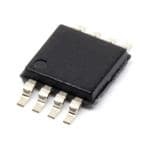
| 产品图片 |
|
| rohs | 符合RoHS无铅 / 符合限制有害物质指令(RoHS)规范要求 |
| 产品系列 | 放大器 IC,精密放大器,Analog Devices AD8676ARMZ- |
| 数据手册 | |
| 产品型号 | AD8676ARMZ |
| 产品培训模块 | http://www.digikey.cn/PTM/IndividualPTM.page?site=cn&lang=zhs&ptm=30008http://www.digikey.cn/PTM/IndividualPTM.page?site=cn&lang=zhs&ptm=26202 |
| 产品种类 | 精密放大器 |
| 供应商器件封装 | 8-MSOP |
| 共模抑制比—最小值 | 130 dB |
| 关闭 | No |
| 包装 | 管件 |
| 压摆率 | 2.5 V/µs |
| 双重电源电压 | +/- 9 V, +/- 12 V |
| 可用增益调整 | 132 dB |
| 商标 | Analog Devices |
| 增益带宽生成 | 10 MHz |
| 增益带宽积 | 10MHz |
| 安装类型 | 表面贴装 |
| 安装风格 | SMD/SMT |
| 封装 | Tube |
| 封装/外壳 | 8-TSSOP,8-MSOP(0.118",3.00mm 宽) |
| 封装/箱体 | MSOP-8 |
| 工作温度 | -40°C ~ 125°C |
| 工作电源电压 | 5 V to 18 V |
| 工厂包装数量 | 50 |
| 放大器类型 | 通用 |
| 最大双重电源电压 | +/- 15 V |
| 最大工作温度 | + 125 C |
| 最小双重电源电压 | +/- 5 V |
| 最小工作温度 | - 40 C |
| 标准包装 | 50 |
| 电压-电源,单/双 (±) | 10 V ~ 36 V, ±5 V ~ 18 V |
| 电压-输入失调 | 12µV |
| 电压增益dB | 126 dB |
| 电流-电源 | 2.7mA |
| 电流-输入偏置 | 2nA |
| 电流-输出/通道 | 20mA |
| 电源电压-最大 | 18 V |
| 电源电压-最小 | 5 V |
| 电源电流 | 2.7 mA |
| 电源类型 | Dual |
| 电路数 | 2 |
| 系列 | AD8676 |
| 视频文件 | http://www.digikey.cn/classic/video.aspx?PlayerID=1364138032001&width=640&height=505&videoID=2245193153001http://www.digikey.cn/classic/video.aspx?PlayerID=1364138032001&width=640&height=505&videoID=2245193159001 |
| 设计资源 | |
| 转换速度 | 2.5 V/us |
| 输入偏压电流—最大 | 4.5 nA |
| 输入电压范围—最大 | 12.5 V |
| 输入补偿电压 | 12 uV |
| 输出电流 | 20 mA |
| 输出类型 | Rail to Rail Output |
| 通道数量 | 2 Channel |


- 商务部:美国ITC正式对集成电路等产品启动337调查
- 曝三星4nm工艺存在良率问题 高通将骁龙8 Gen1或转产台积电
- 太阳诱电将投资9.5亿元在常州建新厂生产MLCC 预计2023年完工
- 英特尔发布欧洲新工厂建设计划 深化IDM 2.0 战略
- 台积电先进制程称霸业界 有大客户加持明年业绩稳了
- 达到5530亿美元!SIA预计今年全球半导体销售额将创下新高
- 英特尔拟将自动驾驶子公司Mobileye上市 估值或超500亿美元
- 三星加码芯片和SET,合并消费电子和移动部门,撤换高东真等 CEO
- 三星电子宣布重大人事变动 还合并消费电子和移动部门
- 海关总署:前11个月进口集成电路产品价值2.52万亿元 增长14.8%


PDF Datasheet 数据手册内容提取
Ultraprecision, 36 V, 2.8 nV/√Hz Dual Rail-to-Rail Output Op Amp Data Sheet AD8676 FEATURES PIN CONFIGURATIONS Very low voltage noise 2.8 nV/√Hz @ 1 kHz OUTA 1 8 V+ Rail-to-rail output swing –INA 2 AD8676 7 OUTB Low input bias current: 2 nA maximum VLoewry i lnopwu ot foffsfeste vt odlrtiaftg: e0:. 162 μ μVV/° Cty mpiacxailm um +INVA– 34 (NToOt Pto V SIEcaWle) 65 –+IINNBB 06487-001 Figure 1. 8-Lead SOIC_N (R-8) Very high gain: 120 dB Wide bandwidth: 10 MHz typical OUT A 1 8 V+ ±5 V to ±18 V operation –IN A 2 AD8676 7 OUT B APrPecPisLiIoCnA inTsItOruNmSe ntation +INV A– 34 (NToOt Pto V SIEcaWle) 65 +–IINN BB 06487-002 Figure 2. 8-Lead MSOP (RM-8) PLL filters Laser diode control loops Strain gage amplifiers Medical instrumentation Thermocouple amplifiers GENERAL DESCRIPTION The AD8676 precision operational amplifier offers ultralow The smaller packages and low power consumption afforded by offset, drift, and voltage noise combined with very low input the AD8676 allow maximum channel density or minimum bias currents over the full operating temperature range. The board size for space-critical equipment. AD8676 is a precision, wide bandwidth op amp featuring rail- The AD8676 is specified for the extended industrial temperature to-rail output swings and very low noise. Operation is fully range (−40°C to +125°C). The AD8676 is available in the 8-lead specified from ±5 V to ±15 V. MSOP, and the popular 8-lead, narrow SOIC; both of which are The AD8676 features a rail-to-rail output like that of the OP184, lead-free packages. MSOP packaged devices are only available but with wide bandwidth and even lower voltage noise, com- in tape and reel format. bined with the precision and low power consumption like that For the single version of this ultraprecision, rail-to-rail op amp, of the industry-standard OP07 amplifier. Unlike other low see the AD8675 data sheet. noise, rail-to-rail op amps, the AD8676 has very low input bias current and low input current noise. The AD8675 and AD8676 are members of a growing series of low noise op amps offered by Analog Devices, Inc. With typical offset voltage of only 12 μV, offset drift of 0.2 μV/°C, and noise of only 0.10 μV p-p (0.1 Hz to 10 Hz), the AD8676 is Table 1. Voltage Noise perfectly suited for applications where large error sources Package 0.9 nV 1.1 nV 1.8 nV 2.8 nV 3.8 nV cannot be tolerated. Precision instrumentation, PLL and other Single AD797 AD8597 ADA4004-1 AD8675 AD8671 precision filter circuits, position and pressure sensors, medical Dual AD8599 ADA4004-2 AD8676 AD8672 instrumentation, and strain gage amplifiers benefit greatly from Quad ADA4004-4 AD8674 the very low noise, low input bias current, and wide bandwidth. Many systems can take advantage of the low noise, dc precision, and rail-to-rail output swing provided by the AD8676 to maxi- mize SNR and dynamic range. Rev. C Information furnished by Analog Devices is believed to be accurate and reliable. However, no responsibility is assumed by Analog Devices for its use, nor for any infringements of patents or other One Technology Way, P.O. Box 9106, Norwood, MA 02062-9106, U.S.A. rights of third parties that may result from its use. Specifications subject to change without notice. No license is granted by implication or otherwise under any patent or patent rights of Analog Devices. Tel: 781.329.4700 www.analog.com Trademarks and registered trademarks are the property of their respective owners. Fax: 781.461.3113 ©2006–2011 Analog Devices, Inc. All rights reserved.
AD8676 Data Sheet TABLE OF CONTENTS Features .............................................................................................. 1 Absolute Maximum Ratings ............................................................5 Applications ....................................................................................... 1 Thermal Resistance .......................................................................5 Pin Configurations ........................................................................... 1 Power Sequencing .........................................................................5 General Description ......................................................................... 1 ESD Caution...................................................................................5 Revision History ............................................................................... 2 Typical Performance Characteristics ..............................................6 Specifications ..................................................................................... 3 Outline Dimensions ....................................................................... 11 Electrical Specifications ............................................................... 3 Ordering Guide .......................................................................... 11 REVISION HISTORY 8/11—Rev. B to Rev. C 4/08—Rev. 0 to Rev. A Change to Y-Axis Label, Figure 9 ................................................... 7 Changes to Table 1 ............................................................................. 3 Changes to Table 2 ............................................................................. 4 11/09—Rev. A to Rev. B Changes to Figure 6, Figure 7, Figure 8 .......................................... 6 Changes to General Description Section ...................................... 1 Changes to Figure 9 through Figure 12 .......................................... 7 Added Table 1; Renumbered Sequentially .................................... 1 Changes to Figure 21, Figure 22, and Figure 25 ............................ 9 Updated Outline Dimensions ....................................................... 11 Added Figure 26, Renumbered Sequentially ................................. 9 Changes to Ordering Guide .......................................................... 11 Changes to Figure 27 ...................................................................... 10 Added Figure 28, Renumbered Sequentially .............................. 10 10/06—Revision 0: Initial Version Rev. C | Page 2 of 12
Data Sheet AD8676 SPECIFICATIONS ELECTRICAL SPECIFICATIONS V = ±5.0 V, V = 0 V, V = 0 V, T = +25°C, unless otherwise specified. S CM O A Table 2. Parameter Symbol Conditions Min Typ Max Unit INPUT CHARACTERISTICS Offset Voltage V OS B Grade (SOIC) 12 50 μV B Grade (MSOP) 60 μV A Grade (SOIC, MSOP) 100 μV Offset Voltage V −40°C ≤ T ≤ +125°C OS A B Grade (SOIC, MSOP) 15 160 μV A Grade (SOIC, MSOP) 250 μV Input Bias Current I −2 +2 nA B −40°C ≤ T ≤ +125°C −5.5 +5.5 nA A Input Offset Current I −1 +1 nA OS −40°C ≤ T ≤ +125°C −2.8 +2.8 nA A Input Voltage Range −3.0 +3.0 V Common-Mode Rejection Ratio CMRR V = −3.0 V to +3.0 V 105 130 dB CM −40°C ≤ T ≤ +125°C 105 dB A Open-Loop Gain A R = 2 kΩ to ground, 120 126 dB VO L V = −3.5 V to +3.5 V O −40°C ≤ T ≤ +125°C 117 dB A Offset Voltage Drift ΔV /ΔT −40°C ≤ T ≤ +125°C 0.2 0.6 μV/°C OS A OUTPUT CHARACTERISTICS Output Voltage High V R = 10 kΩ to ground +4.90 +4.95 V OH L −40°C ≤ T ≤ +125°C +4.85 V A R = 2 kΩ to ground +4.80 +4.89 V L −40°C ≤ T ≤ +125°C +4.75 V A Output Voltage Low V R = 10 kΩ to ground −4.98 −4.90 V OL L −40°C ≤ T ≤ +125°C −4.85 V A R = 2 kΩ to ground −4.91 −4.86 V L −40°C ≤ T ≤ +125°C −4.82 V A Short-Circuit Limit I +40 mA SC Output Current I ±20 mA O POWER SUPPLY Power Supply Rejection Ratio PSRR V = ±5.0 V to ±15.0 V 106 120 dB S −40°C ≤ T ≤ +125°C 106 120 dB A Supply Current/Amplifier I V = 0 V 2.5 3.2 mA SY O −40°C ≤ T ≤ +125°C 3.8 mA A DYNAMIC PERFORMANCE Slew Rate SR R = 2 kΩ 2.5 V/μs L Gain Bandwidth Product GBP 10 MHz NOISE PERFORMANCE Voltage Noise e p-p 0.1 Hz to 10 Hz 0.1 μV p-p n Voltage Noise Density e f = 1 kHz 2.8 nV/√Hz n Current Noise Density i f = 10 Hz 0.3 pA/√Hz n Rev. C | Page 3 of 12
AD8676 Data Sheet V = ±15 V, V = 0 V, V = 0 V, T = +25°C, unless otherwise specified. S CM O A Table 3. Parameter Symbol Conditions Min Typ Max Unit INPUT CHARACTERISTICS Offset Voltage V OS B Grade (SOIC) 12 50 μV B Grade (MSOP) 60 μV A Grade (SOIC, MSOP) 100 μV Offset Voltage V −40°C ≤ T ≤ +125°C OS A B Grade (SOIC, MSOP) 15 160 μV A Grade (SOIC, MSOP) 250 μV Input Bias Current I −2 +2 nA B −40°C ≤ T ≤ +125°C −4.5 +4.5 nA A Input Offset Current I −1 +1 nA OS −40°C ≤ T ≤ +125°C −2.8 +2.8 nA A Input Voltage Range −12.5 +12.5 V Common-Mode Rejection Ratio CMRR V = −12.5 V to +12.5 V 111 130 dB CM −40°C ≤ T ≤ +125°C 107 130 dB A Open-Loop Gain A R = 2 kΩ to ground, 123 132 dB VO L V = −13.5 V to +13.5 V O −40°C ≤ T ≤ +125°C 117 dB A Offset Voltage Drift ΔV /ΔT −40°C ≤ T ≤ +125°C 0.2 0.6 μV/°C OS A OUTPUT CHARACTERISTICS Output Voltage High V R = 10 kΩ to ground +14.85 +14.92 V OH L −40°C ≤ T ≤ +125°C +14.80 V A R = 2 kΩ to ground +14.60 +14.75 V L −40°C ≤ T ≤ +125°C +14.40 V A Output Voltage Low V R = 10 kΩ to ground −14.96 −14.94 V OL L −40°C ≤ T ≤ +125°C −14.90 V A R = 2 kΩ to ground −14.85 −14.75 V L −40°C ≤ T ≤ +125°C −14.60 V A Short-Circuit Limit I +40 mA SC Output Current I ±20 mA O POWER SUPPLY Power Supply Rejection Ratio PSRR V = ±5.0 V to ±15.0 V 106 120 dB S −40°C ≤ T ≤ +125°C 106 dB A Supply Current/Amplifier I V = 0 V 2.7 3.4 mA SY O −40°C ≤ T ≤ +125°C 4.2 mA A DYNAMIC PERFORMANCE Slew Rate SR R =10 kΩ 2.5 V/μs L Gain Bandwidth Product GBP 10 MHz NOISE PERFORMANCE Voltage Noise e p-p 0.1 Hz to 10 Hz 0.1 μV p-p n Voltage Noise Density e f = 1 kHz 2.8 nV/√Hz n Current Noise Density i f = 10 Hz 0.3 pA/√Hz n Rev. C | Page 4 of 12
Data Sheet AD8676 ABSOLUTE MAXIMUM RATINGS THERMAL RESISTANCE Table 4. Parameter Rating Table 5. Thermal Resistance Supply Voltage ±18 V Package Type θ θ Unit JA JC Input Voltage ±V supply 8-Lead MSOP (RM) 210 45 °C/W Differential Input Voltage ±0.7 V 8-Lead SOIC_N (R) 158 43 °C/W Output Short-Circuit Duration to GND Indefinite Storage Temperature Range RM, R Packages −65°C to +150°C POWER SEQUENCING Operating Temperature Range −40°C to +125°C The op amp supplies must be established simultaneously with, Junction Temperature Range or before, any input signals are applied. If this is not possible, RM, R Packages −65°C to +150°C the input current must be limited to 10 mA. Lead Temperature Range (Soldering, 10 sec) 300°C ESD CAUTION Stresses above those listed under Absolute Maximum Ratings may cause permanent damage to the device. This is a stress rating only; functional operation of the device at these or any other conditions above those indicated in the operational section of this specification is not implied. Exposure to absolute maximum rating conditions for extended periods may affect device reliability. Rev. C | Page 5 of 12
AD8676 Data Sheet TYPICAL PERFORMANCE CHARACTERISTICS ±15 V and ±5 V, T = 25°C, unless otherwise specified. A 10 150 VS = ±15V 9 Hz) 8 100 V/ Y (n 7 50 T OISE DENSI 654 V (µV)OS 0 TYPICAL N E –50 G 3 A T VOL 2 –100 1 0 –150 1 10 F1R0E0QUENCY (1Hkz) 10k 100k 06487-003 –40 –20 0 T2E0MPER4A0TURE6 (0°C) 80 100 120 06487-106 Figure 3. Voltage Noise Density vs. Frequency Figure 6. Offset Voltage vs. Temperature 90 350 80 300 70 RS RS 250 MPLIFIE 6500 MPLIFIE 200 A A R OF 40 R OF 150 MBE 30 MBE U U 10 N N 20 50 10 0 0 –100 –80 –60 –40 –20VOS0 (µV)20 40 60 80 100 06487-004 –2.0 –1.6 –1.2 –0.8 –0.4 IB0 (nA0).4 0.8 1.2 1.6 2.0 06487-107 Figure 4. Input Offset Voltage Distribution Figure 7. Input Bias Current, VSY = ±15 V 25 350 300 20 RS RS 250 MPLIFIE 15 MPLIFIE 200 A A R OF 10 R OF 150 BE BE M M NU NU 10 5 50 0 0 00.050.100.150.200.250.300.35T0.40CV0.45OS0.50 (µV0.55/°C0.60)0.650.70 0.750.800.850.900.951.00 06487-005 –2.0 –1.6 –1.2 –0.8 –0.4 IB0 (nA0).4 0.8 1.2 1.6 2.0 06487-108 Figure 5. TCVOS Distribution Figure 8. Input Bias Current, VSY = ±5 V Rev. C | Page 6 of 12
Data Sheet AD8676 ±15 V and ±5 V, T = 25°C, unless otherwise specified. A 5 120 180 4 100 GAIN RCLL == 23k5pΩF 135 80 θM = 55.2° 3 60 90 s) A) 12 dB) 4200 PHASE 45 N (Degree I (nB –10 VS = ±5V GAIN ( –200 0 MARGI VS = ±15V –40 –45 SE –2 A H –60 –90 P –3 –80 –135 –4 –100 –5 –120 –180 –40 –20 0 T2E0MPER4A0TURE6 (0°C) 80 100 120 06487-109 100 1k 10kFREQU1E0N0kCY (Hz)1M 10M 100M 06487-012 Figure 9. Input Bias Current vs. Temperature Figure 12. Gain and Phase vs. Frequency 3.0 60 50 2.5 40 RENT (mA) 2.0 P GAIN (dB) 3200 GG == 11000 R 1.5 O 10 U O C L Y D- 0 SUPPL 1.0 CLOSE –10 G = 1 –20 0.5 –30 0 –40 5 10 15SUPPLY 2V0OLTAGE2 (5V) 30 35 06487-110 1k 10k F1R00EkQUENCY (1HMz) 10M 100M 06487-013 Figure 10. Supply Current vs. Total Supply Voltage Figure 13. Closed-Loop Gain vs. Frequency 4.0 70 3.5 60 VS = ±15V 3.0 A) 50 m T ( 2.5 URREN 2.0 VS = ±5V (Ω)UT 40 AVO= 100 C O LY 1.5 Z 30 AVO= 10 P P SU 1.0 20 AVO= 1 0.5 10 0 0 –40 –20 0 T2E0MPER4A0TURE6 (0°C) 80 100 120 06487-111 1k 10k F1R00EkQUENCY 1(HMz) 10M 100M 06487-014 Figure 11. Supply Current vs. Temperature Figure 14. ZOUT vs. Frequency Rev. C | Page 7 of 12
AD8676 Data Sheet ±15 V and ±5 V, T = 25°C, unless otherwise specified. A 15 0.1 50 VIN = ±10V RL = 2kΩ VIN AV = +1 0 40 10 –0.1 30 E (V) 5 AGE (V) –0.2 20 TAGE (V) OLTAG 0 T VOLT –0.3 10 UT VOL V U –0.4 0 P –5 INP VOUT OUT –0.5 –10 –10 –0.6 VAIVNO = = 2 –0100m0V p-p –20 RL = 10kΩ –15 –0.7 –30 TIME (10µs/DIV) 06487-015 –4 1 6 11 TIM1E6 (µs) 21 26 31 36 06487-018 Figure 15. Large Signal Transient Response, VSY = ±15 V Figure 18. Positive Overvoltage Recovery 4 0.3 50 VIN = ±3.5V VIN = 200mV p-p 3 ARLV == 2+k1Ω 0.2 RAVL O= =1 0–k1Ω00 40 2 0.1 30 E (V) 1 AGE (V) 0 VIN 20 TAGE (V) OLTAG 0 T VOLT –0.1 10 UT VOL V –1 U –0.2 0 P P T IN VOUT OU –2 –0.3 –10 –3 –0.4 –20 –4 –0.5 –30 TIME (10µs/DIV) 06487-016 –4 1 6 11 TIM1E6 (µs) 21 26 31 36 06487-019 Figure 16. Large Signal Transient Response, VSY = ±5 V Figure 19. Negative Overvoltage Recovery 70 180 AV = +1 VIN = 100mV p-p 160 60 140 50 120 %) OT ( 40 dB) 100 RSHO 30 +OS MRR ( 80 E C 60 V O –OS 20 40 20 10 0 0 –20 1 10 CA1P00ACITANCE 1(kpF) 10k 100k 06487-017 10 100 1k FR1E0QkUENC1Y0 0(Hkz) 1M 10M 100M 06487-020 Figure 17. Small Signal Overshoot vs. Load Capacitance Figure 20. CMRR vs. Frequency Rev. C | Page 8 of 12
Data Sheet AD8676 ±15 V and ±5 V, T = 25°C, unless otherwise specified. A 160 1000 B) 140 d O ( TI 120 A SOURCE R N 100 100 TIO –PSRR mV) LY REJEC 6800 +PSRR – V (SOUT P V UP 40 10 SINK S ER 20 W O P 0 –20 1 10 100 1k FR1E0QkUENC1Y0 0(Hkz) 1M 10M 100M 06487-021 0.001 0.01 LOA0D.1 CURRENT 1(mA) 10 100 06487-024 Figure 21. Power Supply Rejection Ratio vs. Frequency Figure 24. Output Saturation Voltage vs. Output Load Current 126 15.0 RL = 2kΩ B) VS = ±15V O (d 124 14.9 TI V) RA 122 E ( CTION 120 OLTAG 14.8 E V Y REJ 118 TPUT 14.7 L U SUPP 116 GH O 14.6 R HI E W 14.5 O 114 P 112 14.4 –40 –20 0 T2E0MPER4A0TURE6 (0°C) 80 100 120 06487-122 –40 –20 0 T2E0MPER4A0TURE6 (0°C) 80 100 120 06487-125 Figure 22. Power Supply Rejection Ratio vs. Temperature Figure 25. High Output Voltage, VOH vs. Temperature, VS = ±15 V 0.06 5.00 RL = 2kΩ VS = ±5V 0.04 4.95 V) E ( 0.02 AG V) LT 4.90 µ O OISE ( 0 PUT V N T 4.85 U –0.02 H O G HI 4.80 –0.04 –0.06 4.75 0 1 2 3 4 TIM5E (s) 6 7 8 9 10 06487-023 –40 –20 0 T2E0MPER4A0TURE6 (0°C) 80 100 120 06487-225 Figure 23. Voltage Noise (0.1 Hz to 10 Hz) Figure 26. High Output Voltage, VOH vs. Temperature, VS = ±5 V Rev. C | Page 9 of 12
AD8676 Data Sheet ±15 V and ±5 V, T = 25°C, unless otherwise specified. A –14.70 –4.93 RL = 2kΩ RL = 2kΩ VS = ±15V VS = ±5V –4.94 –14.75 V) V) E ( E ( –4.95 G –14.80 G A A T T OL OL –4.96 V V T –14.85 T U U P P –4.97 T T U U O –14.90 O W W –4.98 O O L L –14.95 –4.99 –15.00 –5.00 –40 –20 0 T2E0MPER4A0TURE6 (0°C) 80 100 120 06487-126 –40 –20 0 T2E0MPER4A0TURE6 (0°C) 80 100 120 06487-226 Figure 27. Low Output Voltage, VOL vs. Temperature, VS = ±15 V Figure 28. Low Output Voltage, VOL vs. Temperature, VS = ±5 V Rev. C | Page 10 of 12
Data Sheet AD8676 OUTLINE DIMENSIONS 5.00(0.1968) 4.80(0.1890) 8 5 4.00 (0.1574) 6.20 (0.2441) 3.80 (0.1497) 1 4 5.80 (0.2284) 1.27 (0.0500) 0.50 (0.0196) BSC 1.75 (0.0688) 0.25 (0.0099) 45° 0.25 (0.0098) 1.35 (0.0532) 8° 0.10 (0.0040) 0° COPLANARITY 0.51 (0.0201) 0.10 SEATING 0.31 (0.0122) 0.25 (0.0098) 10..2470 ((00..00510507)) PLANE 0.17 (0.0067) COMPLIANTTO JEDEC STANDARDS MS-012-AA C(RINOEFNPETARRREOENNLCLTEIHN EOGSN DELSIYM)AEANNRDSEI AORRNOESU NANORDEET DAIN-PO MPFRIFLO LMPIIMRLELIATIMTEEER TFSEO; RIRN ECUQHSU EDI VIINMA LEDENENSSTIIOGSN NFS.OR 012407-A Figure 29. 8-Lead Standard Small Outline Package [SOIC_N] Narrow Body (R-8) Dimensions shown in millimeters and (inches) 3.20 3.00 2.80 8 5 5.15 3.20 4.90 3.00 4.65 2.80 1 4 PIN1 IDENTIFIER 0.65BSC 0.95 15°MAX 0.85 1.10MAX 0.75 0.80 0.15 0.40 6° 0.23 0.55 CO0P.0L5ANARITY 0.25 0° 0.09 0.40 0.10 COMPLIANTTOJEDECSTANDARDSMO-187-AA 100709-B Figure 30. 8-Lead Mini Small Outline Package [MSOP] (RM-8) Dimensions shown in millimeters ORDERING GUIDE Model1 Temperature Range Package Description Package Option Branding AD8676ARMZ −40°C to +125°C 8-Lead Mini Small Outline Package [MSOP] RM-8 A13 AD8676ARMZ-REEL −40°C to +125°C 8-Lead Mini Small Outline Package [MSOP] RM-8 A13 AD8676ARZ −40°C to +125°C 8-Lead Standard Small Outline Package [SOIC_N] R-8 AD8676ARZ-REEL −40°C to +125°C 8-Lead Standard Small Outline Package [SOIC_N] R-8 AD8676ARZ-REEL7 −40°C to +125°C 8-Lead Standard Small Outline Package [SOIC_N] R-8 AD8676BRMZ −40°C to +125°C 8-Lead Mini Small Outline Package [MSOP] RM-8 A1L AD8676BRMZ-REEL −40°C to +125°C 8-Lead Mini Small Outline Package [MSOP] RM-8 A1L AD8676BRZ −40°C to +125°C 8-Lead Standard Small Outline Package [SOIC_N] R-8 AD8676BRZ-REEL −40°C to +125°C 8-Lead Standard Small Outline Package [SOIC_N] R-8 AD8676BRZ-REEL7 −40°C to +125°C 8-Lead Standard Small Outline Package [SOIC_N] R-8 1 Z = RoHs Compliant Part. Rev. C | Page 11 of 12
AD8676 Data Sheet NOTES ©2006–2011 Analog Devices, Inc. All rights reserved. Trademarks and registered trademarks are the property of their respective owners. D06487-0-8/11(C) Rev. C | Page 12 of 12
Mouser Electronics Authorized Distributor Click to View Pricing, Inventory, Delivery & Lifecycle Information: A nalog Devices Inc.: AD8676ARMZ AD8676ARMZ-REEL AD8676ARZ AD8676BRMZ AD8676BRZ AD8676ARZ-REEL AD8676ARZ- REEL7 AD8676BRMZ-REEL AD8676BRZ-REEL AD8676BRZ-REEL7