ICGOO在线商城 > 集成电路(IC) > 线性 - 放大器 - 仪表,运算放大器,缓冲器放大器 > TLV2372QDRG4Q1

 Datasheet下载
- 型号: TLV2372QDRG4Q1
- 制造商: Texas Instruments
- 库位|库存: xxxx|xxxx
- 要求:
| 数量阶梯 | 香港交货 | 国内含税 |
| +xxxx | $xxxx | ¥xxxx |
查看当月历史价格
查看今年历史价格
TLV2372QDRG4Q1产品简介:
ICGOO电子元器件商城为您提供TLV2372QDRG4Q1由Texas Instruments设计生产,在icgoo商城现货销售,并且可以通过原厂、代理商等渠道进行代购。 TLV2372QDRG4Q1价格参考。Texas InstrumentsTLV2372QDRG4Q1封装/规格:线性 - 放大器 - 仪表,运算放大器,缓冲器放大器, 通用 放大器 2 电路 满摆幅 8-SOIC。您可以下载TLV2372QDRG4Q1参考资料、Datasheet数据手册功能说明书,资料中有TLV2372QDRG4Q1 详细功能的应用电路图电压和使用方法及教程。
Texas Instruments(德州仪器)的TLV2372QDRG4Q1是一款双通道低功耗运算放大器,属于线性放大器系列中的仪表、运算和缓冲放大器类别。它适用于多种场景,尤其是在需要高精度、低功耗以及宽电源电压范围的应用中。以下是其主要应用场景:

 1. 工业自动化与控制
   - TLV2372QDRG4Q1可用于工业传感器信号调理电路中,例如温度、压力或位移传感器的信号放大。
   - 在数据采集系统中,作为前置放大器对微弱信号进行放大,同时保持低噪声特性。
   - 适用于可编程逻辑控制器(PLC)中的模拟输入/输出模块。

 2. 汽车电子
   - 该器件符合AEC-Q100标准,适合汽车级应用,如车载传感器信号处理。
   - 可用于汽车音响系统的音频信号放大,提供清晰的声音输出。
   - 在电池管理系统(BMS)中,用于监测电池电压和电流的变化。

 3. 消费电子产品
   - 在便携式设备(如智能手机、平板电脑)中,用作音频信号放大或传感器信号调理。
   - 适用于家用健康设备(如血压计、血糖仪),对生物医学信号进行精确放大。

 4. 通信设备
   - 用于射频(RF)前端电路中的信号调理,支持低功耗运行。
   - 在无线传感器网络中,放大来自传感器的弱电信号以提高传输质量。

 5. 医疗设备
   - 用于心电图(ECG)、脑电图(EEG)等医疗监测设备,对微弱生理信号进行放大和滤波。
   - 在超声波设备中,作为接收端的前置放大器,提升图像质量。

 6. 测试与测量
   - 在示波器、万用表等测试仪器中,用作信号放大和隔离,确保测量结果的准确性。
   - 适用于高精度数据记录仪,对环境参数(如湿度、光照强度)进行实时监控。

 特性总结
- 低功耗:适合电池供电设备,延长续航时间。
- 宽电源电压范围(2.7V至5.5V):适应多种供电条件。
- 轨到轨输入/输出:提供更大的动态范围,适合复杂信号处理。
- 高增益带宽积(10MHz):支持高频信号放大。

总之,TLV2372QDRG4Q1凭借其优异的性能和可靠性,广泛应用于工业、汽车、消费电子、通信和医疗等领域,为各种精密信号处理任务提供了理想的解决方案。
| 参数 | 数值 |
| -3db带宽 | - |
| 产品目录 | 集成电路 (IC)半导体 |
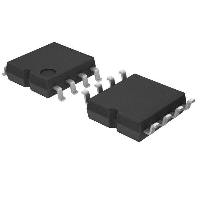
| 描述 | IC OPAMP GP 3MHZ RRO 8SOIC运算放大器 - 运放 Auto Cat 550uA/Ch 3MHz Rail to Rail |
| 产品分类 | Linear - Amplifiers - Instrumentation, OP Amps, Buffer Amps集成电路 - IC |
| 品牌 | Texas Instruments |
| 产品手册 | |
| 产品图片 |
|
| rohs | 符合RoHS无铅 / 符合限制有害物质指令(RoHS)规范要求 |
| 产品系列 | 放大器 IC,运算放大器 - 运放,Texas Instruments TLV2372QDRG4Q1- |
| 数据手册 | |
| 产品型号 | TLV2372QDRG4Q1 |
| 产品种类 | 运算放大器 - 运放 |
| 供应商器件封装 | 8-SOIC |
| 共模抑制比—最小值 | 67 dB |
| 关闭 | No Shutdown |
| 其它名称 | 296-22845-6 |
| 包装 | Digi-Reel® |
| 单位重量 | 72.600 mg |
| 压摆率 | 2.1 V/µs |
| 双重电源电压 | +/- 3 V, +/- 5 V |
| 商标 | Texas Instruments |
| 增益带宽生成 | 3 MHz |
| 增益带宽积 | 3MHz |
| 安装类型 | 表面贴装 |
| 安装风格 | SMD/SMT |
| 封装 | Reel |
| 封装/外壳 | 8-SOIC(0.154",3.90mm 宽) |
| 封装/箱体 | SOIC-8 |
| 工作温度 | -40°C ~ 125°C |
| 工作电源电压 | 2.7 V to 16 V, +/- 1.35 V to +/- 8 V |
| 工厂包装数量 | 2500 |
| 技术 | CMOS |
| 放大器类型 | 通用 |
| 最大双重电源电压 | +/- 8 V |
| 最大工作温度 | + 125 C |
| 最小双重电源电压 | +/- 1.35 V |
| 最小工作温度 | - 40 C |
| 标准包装 | 1 |
| 电压-电源,单/双 (±) | 2.7 V ~ 16 V, ±1.35 V ~ 8 V |
| 电压-输入失调 | 2mV |
| 电流-电源 | 750µA |
| 电流-输入偏置 | 1pA |
| 电流-输出/通道 | 16mA |
| 电源电流 | 1.8 mA |
| 电路数 | 2 |
| 系列 | TLV2372-Q1 |
| 设计资源 | http://www.digikey.com/product-highlights/cn/zh/texas-instruments-webench-design-center/3176 |
| 转换速度 | 2.4 V/us |
| 输入偏压电流—最大 | 60 pA |
| 输入参考电压噪声 | 39 nV |
| 输入补偿电压 | 4.5 mV |
| 输出电流 | 16 mA |
| 输出类型 | 满摆幅 |
| 通道数量 | 2 Channel |


- 商务部:美国ITC正式对集成电路等产品启动337调查
- 曝三星4nm工艺存在良率问题 高通将骁龙8 Gen1或转产台积电
- 太阳诱电将投资9.5亿元在常州建新厂生产MLCC 预计2023年完工
- 英特尔发布欧洲新工厂建设计划 深化IDM 2.0 战略
- 台积电先进制程称霸业界 有大客户加持明年业绩稳了
- 达到5530亿美元!SIA预计今年全球半导体销售额将创下新高
- 英特尔拟将自动驾驶子公司Mobileye上市 估值或超500亿美元
- 三星加码芯片和SET,合并消费电子和移动部门,撤换高东真等 CEO
- 三星电子宣布重大人事变动 还合并消费电子和移动部门
- 海关总署:前11个月进口集成电路产品价值2.52万亿元 增长14.8%


PDF Datasheet 数据手册内容提取
Product Sample & Technical Tools & Support & Folder Buy Documents Software Community TLV2371-Q1,TLV2372-Q1,TLV2374-Q1 SGLS244B–MAY2004–REVISEDDECEMBER2016 TLV237x-Q1 550-µA/Channel, 3-MHz Rail-to-Rail Input and Output Operational Amplifiers 1 Features 3 Description • QualifiedforAutomotiveApplications The TLV237x-Q1 devices are single-supply 1 operational amplifiers providing rail-to-rail input and • AEC-Q100QualifiedWiththeFollowingResults: output capability. The TLV237x-Q1 takes the – DeviceTemperatureGrade1: –40°Cto125°C minimum operating supply voltage down to 2.7 V and AmbientOperatingTemperatureRange up to 16 V over the extended automotive temperature – DeviceHBMESDClassificationLevel2 range. Therefore, the wide voltage range can support both start-stop functionality and a connection directly – DeviceCDMESDClassificationLevelC4B to the typical 12-V battery. The rail-to-rail capabilities • Rail-to-RailInputandOutput allow the device to maximize the output signal and • WideBandwidth:3MHz avoidclipping. • HighSlewRate:2.4V/µs The CMOS inputs enable high-impedance suitable for • SupplyVoltageRange:2.7Vto16V engine control units (ECU), body control modules (BCM), battery management systems (BMS), and • SupplyCurrent:550µA/Channel HEV/EV inverters. This also allows the user to draw a • InputNoiseVoltage:39nV/√Hz lower offset voltage and maintain low power • InputBiasCurrent:1pA consumption to help meet overall system needs for quiescent current such as in infotainment or cluster, • Ultra-SmallPackaging: HEV/EV,andpowertrain. – 5-PinSOT-23(TLV2371-Q1) Additionally, the TLV237x-Q1 family supports a high 2 Applications common-mode rail to the supply voltage. This feature sets no gain limitations and can support the input at • EngineControlUnits(ECU) anylevelwithouttheconcernforanyphasereversal. • BodyControlModules(BCM) DeviceInformation(1) • BatteryManagementSystems PARTNUMBER PACKAGE BODYSIZE(NOM) • HEV/EVInverters SOT-23(5) 2.90mm×1.60mm • LaneDepartureWarning TLV2371-Q1 SOIC(8) 4.90mm×3.91mm • WhiteGoods TLV2372-Q1 SOIC(8) 4.90mm×3.91mm SOIC(14) 8.65mm×3.91mm TLV2374-Q1 TSSOP(14) 5.00mm×4.40mm (1) For all available packages, see the orderable addendum at theendofthedatasheet. OutputVoltagevsDifferentialInput inHighCurrentSensing 12 11 10 s 9 olt V 8 n e i 7 g a 6 olt V 5 put 4 ut O 3 2 VOUT in Volts 1 VOUT Ideal 0 0 100 200 300 400 500 600 Voltage Across The Sense Resistor in mV D001 1 An IMPORTANT NOTICE at the end of this data sheet addresses availability, warranty, changes, use in safety-critical applications, intellectualpropertymattersandotherimportantdisclaimers.PRODUCTIONDATA.
TLV2371-Q1,TLV2372-Q1,TLV2374-Q1 SGLS244B–MAY2004–REVISEDDECEMBER2016 www.ti.com Table of Contents 1 Features.................................................................. 1 8.3 FeatureDescription.................................................15 2 Applications........................................................... 1 8.4 DeviceFunctionalModes........................................17 3 Description............................................................. 1 9 ApplicationandImplementation........................ 18 4 RevisionHistory..................................................... 2 9.1 ApplicationInformation............................................18 9.2 TypicalApplications................................................18 5 DeviceComparisonTable..................................... 3 10 PowerSupplyRecommendations..................... 21 6 PinConfigurationandFunctions......................... 3 11 Layout................................................................... 22 7 Specifications......................................................... 5 11.1 LayoutGuidelines.................................................22 7.1 AbsoluteMaximumRatings......................................5 11.2 LayoutExamples...................................................23 7.2 ESDRatings..............................................................5 11.3 PowerDissipationConsiderations........................23 7.3 RecommendedOperatingConditions.......................5 12 DeviceandDocumentationSupport................. 24 7.4 ThermalInformation:TLV2371-Q1...........................6 7.5 ThermalInformation:TLV2372-Q1...........................6 12.1 RelatedLinks........................................................24 7.6 ThermalInformation:TLV2374-Q1...........................6 12.2 ReceivingNotificationofDocumentationUpdates24 7.7 ElectricalCharacteristics...........................................6 12.3 CommunityResources..........................................24 7.8 TypicalCharacteristics..............................................9 12.4 Trademarks...........................................................24 12.5 ElectrostaticDischargeCaution............................24 8 DetailedDescription............................................ 15 12.6 Glossary................................................................24 8.1 Overview.................................................................15 13 Mechanical,Packaging,andOrderable 8.2 FunctionalBlockDiagram.......................................15 Information........................................................... 24 4 Revision History NOTE:Pagenumbersforpreviousrevisionsmaydifferfrompagenumbersinthecurrentversion. ChangesfromRevisionA(June2008)toRevisionB Page • AddedESDRatingstable,FeatureDescriptionsection,DeviceFunctionalModes,ApplicationandImplementation section,PowerSupplyRecommendationssection,Layoutsection,DeviceandDocumentationSupportsection,and Mechanical,Packaging,andOrderableInformationsection.................................................................................................. 1 • Deleted8-PinMSOP(TLV2372)becausetheTLV2372-Q1isnotavailableinMSOP;alsoremovedallreferences throughoutthedatasheet....................................................................................................................................................... 1 • ChangedlistitemsinApplications......................................................................................................................................... 1 • RemovedFamilyPackageandAvailableOptionstables,seePOAattheendofthedatasheet ........................................ 1 • RenamedSelectionofSignalAmplifierProductstabletoDeviceComparisonTable............................................................ 3 • ChangedSHUTDOWNfortheTLV237xintheDeviceComparisonTableFrom:YesTo:—............................................... 3 • ChangedI (pA)fortheTLV246xintheDeviceComparisonTableFrom:1300To:1.3...................................................... 3 IB • ChangedSHUTDOWNfortheTLV237xintheDeviceComparisonTableFrom:YesTo:—............................................... 3 • ChangedGNDDESCRIPTIONinPinFunctions:TLV2371-Q1From:GroundconnectionTo:Negative(lowest) powersupply........................................................................................................................................................................... 3 • ChangedGNDDESCRIPTIONinPinFunctions:TLV2372-Q1From:GroundconnectionTo:Negative(lowest) powersupply........................................................................................................................................................................... 4 • RemovedTypicalPin1Indicatorsimage .............................................................................................................................. 4 • ChangedGNDDESCRIPTIONinPinFunctions:TLV2374-Q1From:GroundconnectionTo:Negative(lowest) powersupply........................................................................................................................................................................... 4 • DeletedLeadtemperature(260°Cmaximum)........................................................................................................................ 5 • AddedadditionalthermalvaluestoallThermalInformationtables........................................................................................ 6 • ChangedR valuesinThermalInformation:TLV2371-Q1From:325.1To:228.5(DBV)andFrom:176To:138.4(D)...6 θJA • ChangedR valueinThermalInformation:TLV2372-Q1From:176To:138.4(D)............................................................ 6 θJA • DeletedentireDGK(MSOP)columnfromThermalInformation:TLV2372-Q1..................................................................... 6 • ChangedR valuesinThermalInformation:TLV2374-Q1From:122.3To:67(D)andFrom:173.6To:121(PW)..........6 θJA • DeletedMaximumPowerDissipationvsFree-AirTemperaturegraph................................................................................ 23 2 SubmitDocumentationFeedback Copyright©2004–2016,TexasInstrumentsIncorporated ProductFolderLinks:TLV2371-Q1 TLV2372-Q1 TLV2374-Q1
TLV2371-Q1,TLV2372-Q1,TLV2374-Q1 www.ti.com SGLS244B–MAY2004–REVISEDDECEMBER2016 5 Device Comparison Table Typicalvaluesmeasuredat5Vand25°C SINGLES, GBW SR RAIL-TO- DEVICE V (V) V (µV) Iq/Ch(µA) I (pA) SHUTDOWN DUALS, DD IO IB (MHz) (V/µs) RAIL QUADS TLV237x-Q1 2.7to16 500 550 1 3 2.4 — I/O S,D,Q TLC227x-Q1 4to16 300 1100 1 2.2 3.6 — O D,Q TLV27x-Q1 2.7to16 500 550 1 3 2.4 — O S,D,Q TLV246x-Q1 2.7to6 150 550 1.3 6.4 1.6 Yes I/O S,D,Q TLV247x-Q1 2.7to6 250 600 2 2.8 1.5 — I/O S,D,Q TLV244x-Q1 2.7to10 300 725 1 1.8 1.4 — O D,Q 6 Pin Configuration and Functions TLV2371-Q1DBVPackage 5-PinSOT-23 TLV2371-Q1DPackage TopView 8-PinSOIC TopView OUT 1 5 VDD NC 1 8 NC GND 2 IN− 2 7 VDD IN+ 3 6 OUT IN+ 3 4 IN− GND 4 5 NC PinFunctions:TLV2371-Q1 PIN I/O DESCRIPTION NAME SOT-23 SOIC GND 2 4 — Negative(lowest)powersupply IN– 4 2 I Negative(inverting)input IN+ 3 3 I Positive(noninverting)input NC — 1,5,8 — Nointernalconnection(canbeleftfloating) OUT 1 6 O Output V 5 7 — Positivepowersupply DD Copyright©2004–2016,TexasInstrumentsIncorporated SubmitDocumentationFeedback 3 ProductFolderLinks:TLV2371-Q1 TLV2372-Q1 TLV2374-Q1
TLV2371-Q1,TLV2372-Q1,TLV2374-Q1 SGLS244B–MAY2004–REVISEDDECEMBER2016 www.ti.com TLV2372-Q1DPackage 8-PinSOIC TopView 1OUT 1 8 VDD 1IN− 2 7 2OUT 1IN+ 3 6 2IN− GND 4 5 2IN+ PinFunctions:TLV2372-Q1 PIN I/O DESCRIPTION NAME NO. 1IN– 2 I Invertinginput,channel1 1IN+ 3 I Noninvertinginput,channel1 1OUT 1 O Output,channel1 2IN– 6 I Invertinginput,channel2 2IN+ 5 I Noninvertinginput,channel2 2OUT 7 O Output,channel2 GND 4 — Negative(lowest)powersupply V 8 — Positivepowersupply DD TLV2374-Q1DandPWPackages 14-PinSOICorTSSOP TopView 1OUT 1 14 4OUT 1IN− 2 13 4IN− 1IN+ 3 12 4IN+ VDD 4 11 GND 2IN+ 5 10 3IN+ 2IN− 6 9 3IN− 2OUT 7 8 3OUT PinFunctions:TLV2374-Q1 PIN I/O DESCRIPTION NAME NO. 1IN– 2 I Invertinginput,channel1 1IN+ 3 I Noninvertinginput,channel1 1OUT 1 O Output,channel1 2IN– 6 I Invertinginput,channel2 2IN+ 5 I Noninvertinginput,channel2 2OUT 7 O Output,channel2 3IN– 9 I Invertinginput,channel3 3IN+ 10 I Noninvertinginput,channel3 3OUT 8 O Output,channel3 4IN– 13 I Invertinginput,channel4 4IN+ 12 I Noninvertinginput,channel4 4OUT 14 O Output,channel4 GND 11 — Negative(lowest)powersupply V 4 — Positivepowersupply DD 4 SubmitDocumentationFeedback Copyright©2004–2016,TexasInstrumentsIncorporated ProductFolderLinks:TLV2371-Q1 TLV2372-Q1 TLV2374-Q1
TLV2371-Q1,TLV2372-Q1,TLV2374-Q1 www.ti.com SGLS244B–MAY2004–REVISEDDECEMBER2016 7 Specifications 7.1 Absolute Maximum Ratings overoperatingfree-airtemperaturerange(unlessotherwisenoted)(1) MIN MAX UNIT Supplyvoltage,V 16.5 V DD Differentialinputvoltage,V ±V ID DD Inputvoltage,V –0.2 V +0.2 V I DD Inputcurrent,I ±10 mA I Outputcurrent,I ±100 mA O Maximumjunctiontemperature,T 150 °C J Storagetemperature,T –65 150 °C stg (1) StressesbeyondthoselistedunderAbsoluteMaximumRatingsmaycausepermanentdamagetothedevice.Thesearestressratings only,whichdonotimplyfunctionaloperationofthedeviceattheseoranyotherconditionsbeyondthoseindicatedunderRecommended OperatingConditions.Exposuretoabsolute-maximum-ratedconditionsforextendedperiodsmayaffectdevicereliability. 7.2 ESD Ratings VALUE UNIT TLV2371-Q1inDBVpackage Human-bodymodel(HBM),perAECQ100-002(1) Allpins ±2000 V(ESD) Electrostaticdischarge Allpins ±500 V Charged-devicemodel(CDM),perAECQ100-011 Cornerpins(1,3,4,and5) ±750 TLV2371-Q1inDpackage Human-bodymodel(HBM),perAECQ100-002(1) Allpins ±2000 V(ESD) Electrostaticdischarge Allpins ±500 V Charged-devicemodel(CDM),perAECQ100-011 Cornerpins(1,4,5,and8) ±750 TLV2372-Q1inDpackage Human-bodymodel(HBM),perAECQ100-002(1) Allpins ±2000 V(ESD) Electrostaticdischarge Allpins ±500 V Charged-devicemodel(CDM),perAECQ100-011 Cornerpins(1,4,5,and8) ±750 TLV2374-Q1inDandPWpackages Human-bodymodel(HBM),perAECQ100-002(1) Allpins ±2000 V(ESD) Electrostaticdischarge Allpins ±500 V Charged-devicemodel(CDM),perAECQ100-011 Cornerpins(1,7,8,and14) ±750 (1) AECQ100-002indicatesthatHBMstressingshallbeinaccordancewiththeANSI/ESDA/JEDECJS-001specification. 7.3 Recommended Operating Conditions overoperatingfree-airtemperaturerange(unlessotherwisenoted) MIN MAX UNIT Singlesupply 2.7 16 V Supplyvoltage V DD Splitsupply ±1.35 ±8 V Common-modeinputvoltage 0 V V ICR DD V Turnonvoltagelevel(relativetoGNDpinvoltage) 2 V (ON) V Turnoffvoltagelevel(relativetoGNDpinvoltage) 0.8 V (OFF) T Operatingfree-airtemperature(Q-suffix) –40 125 °C A Copyright©2004–2016,TexasInstrumentsIncorporated SubmitDocumentationFeedback 5 ProductFolderLinks:TLV2371-Q1 TLV2372-Q1 TLV2374-Q1
TLV2371-Q1,TLV2372-Q1,TLV2374-Q1 SGLS244B–MAY2004–REVISEDDECEMBER2016 www.ti.com 7.4 Thermal Information: TLV2371-Q1 TLV2371-Q1 THERMALMETRIC(1) DBV(SOT-23) D(SOIC) UNIT 5PINS 8PINS R Junction-to-ambientthermalresistance 228.5 138.4 °C/W θJA R Junction-to-case(top)thermalresistance 99.1 89.5 °C/W θJC(top) R Junction-to-boardthermalresistance 54.6 78.6 °C/W θJB ψ Junction-to-topcharacterizationparameter 7.7 29.9 °C/W JT ψ Junction-to-boardcharacterizationparameter 53.8 78.1 °C/W JB R Junction-to-case(bottom)thermalresistance — — °C/W θJC(bot) (1) Formoreinformationabouttraditionalandnewthermalmetrics,seetheSemiconductorandICPackageThermalMetricsapplication report. 7.5 Thermal Information: TLV2372-Q1 TLV2372-Q1 THERMALMETRIC(1) D(SOIC) UNIT 8PINS R Junction-to-ambientthermalresistance 138.4 °C/W θJA R Junction-to-case(top)thermalresistance 89.5 °C/W θJC(top) R Junction-to-boardthermalresistance 78.6 °C/W θJB ψ Junction-to-topcharacterizationparameter 29.9 °C/W JT ψ Junction-to-boardcharacterizationparameter 78.1 °C/W JB R Junction-to-case(bottom)thermalresistance — °C/W θJC(bot) (1) Formoreinformationabouttraditionalandnewthermalmetrics,seetheSemiconductorandICPackageThermalMetricsapplication report. 7.6 Thermal Information: TLV2374-Q1 TLV2374-Q1 THERMALMETRIC(1) D(SOIC) PW(TSSOP) UNIT 14PINS 14PINS R Junction-to-ambientthermalresistance 67 121 °C/W θJA R Junction-to-case(top)thermalresistance 24.1 49.4 °C/W θJC(top) R Junction-to-boardthermalresistance 22.5 62.8 °C/W θJB ψ Junction-to-topcharacterizationparameter 2.2 5.9 °C/W JT ψ Junction-to-boardcharacterizationparameter 22.1 62.2 °C/W JB R Junction-to-case(bottom)thermalresistance — — °C/W θJC(bot) (1) Formoreinformationabouttraditionalandnewthermalmetrics,seetheSemiconductorandICPackageThermalMetricsapplication report. 7.7 Electrical Characteristics atspecifiedfree-airtemperature,V =2.7V,5V,and15V(unlessotherwisenoted) DD PARAMETER TESTCONDITIONS MIN TYP MAX UNIT DCPERFORMANCE T =25°C 2 4.5 A V Inputoffsetvoltage V =V /2,V =V /2,R =50Ω mV IO IC DD O DD S T =–40°Cto125°C 6 A α Offsetvoltagedrift V =V /2,V =V /2,R =50Ω,T =25°C 2 µV/°C VIO IC DD O DD S A 6 SubmitDocumentationFeedback Copyright©2004–2016,TexasInstrumentsIncorporated ProductFolderLinks:TLV2371-Q1 TLV2372-Q1 TLV2374-Q1
TLV2371-Q1,TLV2372-Q1,TLV2374-Q1 www.ti.com SGLS244B–MAY2004–REVISEDDECEMBER2016 Electrical Characteristics (continued) atspecifiedfree-airtemperature,V =2.7V,5V,and15V(unlessotherwisenoted) DD PARAMETER TESTCONDITIONS MIN TYP MAX UNIT VIC=0toVDD, TA=25°C 50 68 RS=50Ω TA=–40°Cto125°C 49 V =2.7V DD V =0to T =25°C 53 70 IC A V –1.35V, DD RS=50Ω TA=–40°Cto125°C 54 VIC=0toVDD, TA=25°C 55 72 Common-mode RS=50Ω TA=–40°Cto125°C 54 CMRR V =5V dB rejectionratio DD VIC=0to TA=25°C 58 80 V –1.35V, DD RS=50Ω TA=–40°Cto125°C 57 VIC=0toVDD, TA=25°C 64 82 RS=50Ω TA=–40°Cto125°C 63 V =15V DD V =0to T =25°C 67 84 IC A V –1.35V, DD RS=50Ω TA=–40°Cto125°C 66 T =25°C 95 106 A V =2.7V DD T =–40°Cto125°C 76 A A Large-signaldifferential VO(PP)=VDD/2, V =5V TA=25°C 80 110 dB VD voltageamplification RS=10Ω DD TA=–40°Cto125°C 82 T =25°C 77 83 A V =15V DD T =–40°Cto125°C 79 A INPUT T =25°C 1 60 A I Inputoffsetcurrent V =15V,V =V /2,V =V /2 pA IO DD IC DD O DD T =–40°Cto125°C 500 A T =25°C 1 60 A I Inputbiascurrent V =15V,V =V /2,V =V /2 pA IB DD IC DD O DD T =–40°Cto125°C 500 A Differentialinput r T =25°C 1000 GΩ i(d) resistance A Common-modeinput C f=21kHz,T =25°C 8 pF IC capacitance A OUTPUT T =25°C 2.55 2.58 A V =2.7V DD T =–40°Cto125°C 2.48 A VIC=VDD/2, TA=25°C 4.9 4.93 I =–1mA, V =5V OH DD VID=1V TA=–40°Cto125°C 4.85 T =25°C 14.92 14.96 A V =15V DD High-leveloutput TA=–40°Cto125°C 14.9 V V OH voltage T =25°C 1.88 2 A V =2.7V DD T =–40°Cto125°C 1.42 A VIC=VDD/2, TA=25°C 4.58 4.68 I =–5mA, V =5V OH DD VID=1V TA=–40°Cto125°C 4.44 T =25°C 14.7 14.8 A V =15V DD T =–40°Cto125°C 14.6 A Copyright©2004–2016,TexasInstrumentsIncorporated SubmitDocumentationFeedback 7 ProductFolderLinks:TLV2371-Q1 TLV2372-Q1 TLV2374-Q1
TLV2371-Q1,TLV2372-Q1,TLV2374-Q1 SGLS244B–MAY2004–REVISEDDECEMBER2016 www.ti.com Electrical Characteristics (continued) atspecifiedfree-airtemperature,V =2.7V,5V,and15V(unlessotherwisenoted) DD PARAMETER TESTCONDITIONS MIN TYP MAX UNIT T =25°C 0.1 0.15 A V =2.7V DD T =–40°Cto125°C 0.22 A VIC=VDD/2, TA=25°C 0.05 0.1 I =1mA, V =5V OH DD VID=1V TA=–40°Cto125°C 0.15 T =25°C 0.05 0.08 A V =15V DD Low-leveloutput TA=–40°Cto125°C 0.1 V V OL voltage T =25°C 0.52 0.7 A V =2.7V DD T =–40°Cto125°C 1.15 A VIC=VDD/2, TA=25°C 0.28 0.4 I =5mA, V =5V OH DD VID=1V TA=–40°Cto125°C 0.54 T =25°C 0.19 0.3 A V =15V DD T =–40°Cto125°C 0.35 A POWERSUPPLY V =2.7V T =25°C 470 560 DD A Supplycurrent VDD=5V TA=25°C 550 660 I V =V /2 µA DD (perchannel) O DD T =25°C 750 900 A V =15V DD T =–40°Cto125°C 1200 A Supplyvoltage T =25°C 70 80 V =2.7Vto15V,V =V /2, A PSRR rejectionratio DD IC DD dB (ΔVDD/ΔVIO) noload TA=–40°Cto125°C 65 DYNAMICPERFORMANCE V =2.7V,T =25°C 2.4 DD A UGBW Unitygainbandwidth RL=2kΩ,CL=10pF VDD=5Vto15V, 3 MHz T =25°C A T =25°C 1.4 2 A V =2.7V DD T =–40°Cto125°C 1 A VO(PP)=VDD/2, TA=25°C 1.4 2.4 SR Slewrateatunitygain R =10kΩ, V =5V V/µs L DD CL=50pF TA=–40°Cto125°C 1.2 T =25°C 1.9 2.1 A V =15V DD T =–40°Cto125°C 1.4 A φ Phasemargin R =2kΩ,C =100pF,T =25°C 65° m L L A Gainmargin R =2kΩ,C =10pF,T =25°C 18 dB L L A V =2.7V,V =1V,A =–1,R =2kΩ,C =10pF, DD (STEP)PP V L L 2.9 0.1%at25°C t Settlingtime µs s V =5Vor15V,V =1V,A =–1,R =2kΩ, DD (STEP)PP V L 2 C =47pF,0.1%at25°C L NOISE/DISTORTIONPERFORMANCE A =1 0.02% V V =2.7V,V =V /2V, DD O(PP) DD A =10 0.05% R =2kΩ,f=10kHz,T =25°C V L A Totalharmonic AV=100 0.18% THD+N distortionplusnoise A =1 0.02% V V =5Vor15V,V =V /2V, DD O(PP) DD A =10 0.09% R =2kΩ,f=10kHz,T =25°C V L A A =100 0.5% V Equivalentinputnoise f=1kHz,TA=25°C 39 V nV√Hz n voltage f=10kHz,T =25°C 35 A Equivalentinputnoise I f=1kHz,T =25°C 0.6 fA√Hz n current A 8 SubmitDocumentationFeedback Copyright©2004–2016,TexasInstrumentsIncorporated ProductFolderLinks:TLV2371-Q1 TLV2372-Q1 TLV2374-Q1
TLV2371-Q1,TLV2372-Q1,TLV2374-Q1 www.ti.com SGLS244B–MAY2004–REVISEDDECEMBER2016 7.8 Typical Characteristics Table1.TableofGraphs FIGURE V Inputoffsetvoltage vsCommon-modeinputvoltage Figure1,Figure2,Figure3 IO CMRR Common-moderejectionratio vsFrequency Figure4 Inputbiasandoffsetcurrent vsFree-airtemperature Figure5 V Low-leveloutputvoltage vsLow-leveloutputcurrent Figure6,Figure8,Figure10 OL V High-leveloutputvoltage vsHigh-leveloutputcurrent Figure7,Figure9,Figure11 OH V Peak-to-peakoutputvoltage vsFrequency Figure12 O(PP) I Supplycurrent vsSupplyvoltage Figure13 DD PSRR Powersupplyrejectionratio vsFrequency Figure14 A Differentialvoltagegain&phase vsFrequency Figure15 VD Gain-bandwidthproduct vsFree-airtemperature Figure16 vsSupplyvoltage Figure17 SR Slewrate vsFree-airtemperature Figure18 φ Phasemargin vsCapacitiveload Figure19 m V Equivalentinputnoisevoltage vsFrequency Figure20 n Voltage-followerlarge-signalpulseresponse Figure21,Figure22 Voltage-followersmall-signalpulseresponse Figure23 Invertinglarge-signalresponse Figure24,Figure25 Invertingsmall-signalresponse Figure26 Crosstalk vsFrequency Figure27 1000 1000 VDD=2.7V VDD= 5 V µV 800 TA= 25°C µV 800 TA= 25°C − − Offset Voltage 460000 Offset Voltage 460000 −Input 200 −Input 200 O 0 O 0 VI VI −200 −200 0 0.4 0.8 1.2 1.6 2 2.4 2.7 0 1 2 3 4 5 VICR−Common-Mode Input Voltage−V VICR−Common-Mode Input Voltage−V Figure1.InputOffsetVoltage Figure2.InputOffsetVoltage vsCommon-ModeInputVoltage vsCommon-ModeInputVoltage Copyright©2004–2016,TexasInstrumentsIncorporated SubmitDocumentationFeedback 9 ProductFolderLinks:TLV2371-Q1 TLV2372-Q1 TLV2374-Q1
TLV2371-Q1,TLV2372-Q1,TLV2374-Q1 SGLS244B–MAY2004–REVISEDDECEMBER2016 www.ti.com 1000 120 B VDD=15V −d µ−V 800 TA= 25°C nRatio 100 VDD= 5 V, 15 V Voltage 600 ejectio 80 Offset 400 ModeR 60 VDD= 2.7 V ut 200 n- 40 p o n m −I m O 0 Co 20 VI − R −200 MR 0 0 2 4 6 8 10 12 1415 C 10 100 1k 10 k 100k 1M VICR−Common-ModeInputVoltage−V f−Frequency−Hz Figure3.InputOffsetVoltage Figure4.Common-ModeRejectionRatio vsCommon-ModeInputVoltage vsFrequency 300 2.80 Current−pA 220500 VVDICD== V 2D.7D /V2, 5 V and 15 V oltage−V 2.420 TAVD=D 1=2 52.°7C V set ut V Off 150 utp 1.60 nput Bias / 10500 ow-Level O 01..8200 TATA= =2 570°C°C I L I−IO 0 −OL 0.40 TA= 0°C /B V TA= 40°C II −50 0 −40−25−105 20 35 50 65 80 95 110125 0 2 4 6 8 10 12 14 16 18 20 22 24 TA−Free-AirTemperature−°C IOL−Low-Level Output Current−mA Figure5.InputBiasandOffsetCurrent Figure6.Low-LevelOutputVoltage vsFree-AirTemperature vsLow-LevelOutputCurrent 2.80 5 V VDD= 2.7 V V 4.50 VDD= 5 V Voltage− 2.420 TA=−40°C Voltage− 3.540 TAT=A 7=0 1°2C5°C Output 1.60 TA= 125°C Output 2.530 −High-Level 01..8200 TA=TA T7A=0° =2C 50°°CC −Low-Level 1.5120 TAT=A 0= °2C5°C H 0.40 L TA=−40°C VO VO 0.50 0 0 0 1 2 3 4 5 6 7 8 9 10 11 12 0 5 10152025303540455055606570 IOH−High-Level Output Current−mA IOL−Low-Level Output Current−mA Figure7.High-LevelOutputVoltage Figure8.Low-LevelOutputVoltage vsHigh-LevelOutputCurrent vsLow-LevelOutputCurrent 10 SubmitDocumentationFeedback Copyright©2004–2016,TexasInstrumentsIncorporated ProductFolderLinks:TLV2371-Q1 TLV2372-Q1 TLV2374-Q1
TLV2371-Q1,TLV2372-Q1,TLV2374-Q1 www.ti.com SGLS244B–MAY2004–REVISEDDECEMBER2016 5 15 High-LevelOutputVoltage−V 1234....55552340000 TAT=A 2=5 °7C0°C TA=−40°CTVAC=C 0=° C5 V −Low-Level Output Voltage−V 111024468 VDDTTTA=TAA =A1==−5=T074 A2V°00C5°°=CC°1C25°C − 1 L VOH 0.50 TA= 125°C VO 2 0 0 0 5 10 15 20 25 30 35 40 45 0 20 40 60 80 100 120 140 160 IOH−High-Level Output Current−mA IOL−Low-Level Output Current−mA Figure9.High-LevelOutputVoltage Figure10.Low-LevelOutputVoltage vsHigh-LevelOutputCurrent vsLow-LevelOutputCurrent 15 V 16 14 VDD= 15 V − 15 −V age 14 VDD= 15 V ge 12 TA=−40°C olt 13 a V 12 High-LevelOutputVolt 10468 TATT=AA 0==° C7205°°CC Peak-to-PeakOutput 1110456789 CTARTAVHLLD==== 2−21=V510 Dk5°0 DΩpC%F= 5 V −OH 2 TA= 125°C −PP) 23 VDD= 2.7 V V O( 1 0 V 0 0 20 40 60 80 100 120 140 160 10 100 1 k 10 k 100 k 1 M 10 M IOH−High-Level Output Current−mA f−Frequency−Hz Figure11.High-LevelOutputVoltage Figure12.Peak-to-PeakOutputVoltage vsHigh-LevelOutputCurrent vsFrequency 1 B 120 0.9 AV= 1 −d TA= 25°C Ch 0.8 VIC= VDD/ 2 TA= 125°C Ratio 100 A/ TA= 70°C n VDD=5V,15V m 0.7 o − cti 80 urrent 00..56 y Reje 60 VDD=2.7V Su−pply C 00..34 TA= 0T°AC= 25°C ower Suppl 40 DD 0.2 TA=−40°C −P 20 I 0.1 RR S 0 P 0 0 1 2 3 4 5 6 7 8 9 101112131415 10 100 1 k 10 k 100 k 1 M VCC−SupplyVoltage−V f−Frequency−Hz Figure13.SupplyCurrentvsSupplyVoltage Figure14.PowerSupplyRejectionRatio vsFrequency Copyright©2004–2016,TexasInstrumentsIncorporated SubmitDocumentationFeedback 11 ProductFolderLinks:TLV2371-Q1 TLV2372-Q1 TLV2374-Q1
TLV2371-Q1,TLV2372-Q1,TLV2374-Q1 SGLS244B–MAY2004–REVISEDDECEMBER2016 www.ti.com 120 180 4 z 100 135 MH 3.5 −dB 80 Phase 90 uct− 3 VDD= 15 V n d Gai 60 45 Pro 2.5 −DiffereAntialVoltageVD −2420000 CTVRADLL===D221=5 05k°ΩpCVFdc Gain −−−01943055Phase−° GBWP−GainBandwidth 01..01255 VDD= 5 V VDD= 2.7 V −40 −180 −40−25−10 5 20 35 50 65 80 95 110 125 10 100 1 k 10 k 100 k 1 M 10 M f−Frequency−Hz TA−Free-AirTemperature−°C Figure15.DifferentialVoltageGainandPhase Figure16.GainBandwidthProduct vsFrequency vsFree-AirTemperature 3 3.5 SR− 2.5 3 s SR− µV/ sµ 2.5 − 2 V/ e − at e 2 w R 1.5 SR+ Rat SR+ e w Sl e1.5 − Sl SR 1 ARVL== 110 kΩ SR− 1 VAVDD= =1 5 V 0.5 CL= 50 pF RL= 10 kΩ TA= 25°C 0.5 CL=50pF VI= 3 V 0 0 2.5 4.5 6.5 8.5 10.5 12.5 14.5 −40−25−10 5 20 35 50 65 80 95 110 125 VCC−SupplyVoltage−V TA−Free-AirTemperature−°C Figure17.SlewRatevsSupplyVoltage Figure18.SlewRatevsFree-AirTemperature 100 z 100 90 VDD= 5 V H 90 VDD=2.7,5,15V RL= 2 kΩ V/ TA=25°C 80 TA= 25°C n 80 AV=OpenLoop − °Margin− 567000 Rnull=100 seVoltage 567000 e oi s N Pha 40 Rnull=0 put 40 30 n 30 Rnull=50 ntI 20 e 20 al v 10 ui 10 q E 0 − 0 10 100 1000 n 10 100 1k 10k 100k CL−Capacitive Load−pF V f−Frequency−Hz Figure19.PhaseMarginvsCapacitiveLoad Figure20.EquivalentInputNoiseVoltage vsFrequency 12 SubmitDocumentationFeedback Copyright©2004–2016,TexasInstrumentsIncorporated ProductFolderLinks:TLV2371-Q1 TLV2372-Q1 TLV2374-Q1
TLV2371-Q1,TLV2372-Q1,TLV2374-Q1 www.ti.com SGLS244B–MAY2004–REVISEDDECEMBER2016 V 4 V 12 V−Input Voltage−I 0123 VI CVVATRAVDILL=D==== 3 =2121 5V0 5k° PΩpCVPF 4 ge−V V−Input Voltage−I 0369 VI CVVATRAVDILL=D==== 9 =2121 5V0 1k° 5PΩpCPFV 12 ge−V 3 Volta 9 Volta 2 ut 6 ut p p VO 01 −OutO VO 03 −OutO V V 0 2 4 6 8 10 12 14 16 18 0 2 4 6 8 10 12 14 16 18 t−Time−µs t−Time−µs Figure21.Voltage-FollowerLarge-Signal Figure22.Voltage-FollowerLarge-Signal PulseResponse PulseResponse V V 4 m 0.12 − V−Input Voltage−I00..00048 VI VVTARCAVDILL=D==== 1 =21 2105 500k°Ω CVpmFVPP 00..0182 age−mV V−Input VoltageI 3210 CVTARVAVIDLL=D==== 3 =2121 5V0 5k° PΩpCVPF VI 3 Voltage−V olt 2 ut VO 0.04 put V 1 Outp 0 ut 0 − O VO VO − O 0 0.2 0.4 0.6 0.8 1 1.2 1.4 1.6 1.8 V 0 22 4 6 8 10 12 14 16 t−Time−µs t−Time−µs Figure23.Voltage-FollowerSmall-Signal Figure24.InvertingLarge-SignalResponse PulseResponse V 12 V − − age 9 age 0.10 −InVput VoltI 630 CVVRAVDILL=D=== 9 −21= V10 k1 pΩp5pF V VI V −IVnput VoltI0.005 CVARVDLLD=== −21=10 k5 ΩpVF VI V TA= 25°C VO 96 Voltage− VTAI== 12050° CmVpp VO 00..015 Voltage− 3 ut ut p p ut 0 ut 0 O O − − O O 0 2 4 6 8 10 12 14 16 V 0 0.5 1 1.5 2 2.5 3 3.5 4 4.5 V t−Time−µs t−Time−µs Figure25.InvertingLarge-SignalResponse Figure26.InvertingSmall-SignalResponse Copyright©2004–2016,TexasInstrumentsIncorporated SubmitDocumentationFeedback 13 ProductFolderLinks:TLV2371-Q1 TLV2372-Q1 TLV2374-Q1
TLV2371-Q1,TLV2372-Q1,TLV2374-Q1 SGLS244B–MAY2004–REVISEDDECEMBER2016 www.ti.com 0 VDD= 2.7, 5, & 15 V −20 VI= VDD/2 AV= 1 −40 RL= 2 kΩ TA= 25°C B −60 d − k al −80 sst CrosstalkinShutdown o Cr −100 −120 Crosstalk −140 10 100 1k 10k 100k f−Frequency−Hz Figure27.CrosstalkvsFrequency 14 SubmitDocumentationFeedback Copyright©2004–2016,TexasInstrumentsIncorporated ProductFolderLinks:TLV2371-Q1 TLV2372-Q1 TLV2374-Q1
TLV2371-Q1,TLV2372-Q1,TLV2374-Q1 www.ti.com SGLS244B–MAY2004–REVISEDDECEMBER2016 8 Detailed Description 8.1 Overview The TLV237x-Q1 single-supply operational amplifiers provide rail-to-rail input and output capability with 3-MHz bandwidth. Consuming only 550 µA, the TLV237x-Q1 is the perfect choice for portable and battery-operated applications. The maximum recommended supply voltage is 16 V, which allows the devices to be operated from a variety of rechargeable cells (±8-V supplies down to ±1.35 V). The rail-to-rail inputs with high input impedance maketheTLV237x-Q1idealforsensorsignal-conditioningapplications. 8.2 Functional Block Diagram V+ Reference Current VIN+ VIN- VBIAS1 ClassAB Control V O Circuitry V BIAS2 V- (Ground) Copyright © 2016,Texas Instruments Incorporated 8.3 Feature Description 8.3.1 Rail-to-RailInputOperation TheTLV237x-Q1inputstageconsistsoftwodifferentialtransistorpairs,NMOSandPMOS,thatoperatetogether to achieve rail-to-rail input operation. The transition point between these two pairs can be seen in Figure 1 through Figure 3 for a 2.7-V, 5-V, and 15-V supply. As the common-mode input voltage approaches the positive supply rail, the input pair switches from the PMOS differential pair to the NMOS differential pair. This transition occursapproximately1.35Vfromthepositiverailandresultsinachangeinoffsetvoltageduetodifferentdevice characteristics between the NMOS and PMOS pairs. If the input signal to the device is large enough to swing between both rails, this transition results in a reduction in common-mode rejection ratio (CMRR). If the input signal does not swing between both rails, it is best to bias the signal in the region where only one input pair is active. This is the region in Figure 1 through Figure 3 where the offset voltage varies slightly across the input range and optimal CMRR can be achieved. This has the greatest impact when operating from a 2.7-V supply voltage. Copyright©2004–2016,TexasInstrumentsIncorporated SubmitDocumentationFeedback 15 ProductFolderLinks:TLV2371-Q1 TLV2372-Q1 TLV2374-Q1
TLV2371-Q1,TLV2372-Q1,TLV2374-Q1 SGLS244B–MAY2004–REVISEDDECEMBER2016 www.ti.com Feature Description (continued) 8.3.2 DrivingaCapacitiveLoad When the amplifier is configured in this manner, capacitive loading directly on the output decreases the device’s phase margin, leading to high-frequency ringing or oscillations. Therefore, for capacitive loads of greater than 10 pF, TI recommends placing a resistor in series (R ) with the output of the amplifier, as shown in Figure 28. NULL Aminimumvalueof20Ω workswellformostapplications. RF RG Input − RNULL Output + CLOAD VDD/2 Figure28. DrivingaCapacitiveLoad 8.3.3 OffsetVoltage The output offset voltage, (V ) is the sum of the input offset volt age (V ) and both input bias currents (I ) OO IO IB times the corresponding gains. The schematic and formula in Figure 29 can be used to calculate the output offsetvoltage. R F I IB− R G + − V V I O + R S I IB+ æ æR öö æ æR öö VOO = VIOçç1+çRF ÷÷÷±IIB+ RSçç1+çRF ÷÷÷±IIB- RF è è G øø è è G øø Figure29. OutputOffsetVoltageModel 8.3.4 GeneralConfigurations When receiving low-level signals, limiting the bandwidth of the incoming signals into the system is often required. The simplest way to accomplish this is to place an RC filter at the noninverting terminal of the amplifier (see Figure30). 16 SubmitDocumentationFeedback Copyright©2004–2016,TexasInstrumentsIncorporated ProductFolderLinks:TLV2371-Q1 TLV2372-Q1 TLV2374-Q1
TLV2371-Q1,TLV2372-Q1,TLV2374-Q1 www.ti.com SGLS244B–MAY2004–REVISEDDECEMBER2016 Feature Description (continued) R R G F V /2 DD − V + O V I R1 C1 1 f = -3dB 2pR1C1 V æ R öæ 1 ö O =ç1+ F ÷ç ÷ VI è RG øè1+sR1C1ø Figure30. Single-PoleLow-PassFilter If even more attenuation is required, a multiple pole filter is required. The Sallen-Key filter can be used for this task (see Figure 31). For best results, the amplifier must have a bandwidth that is 8 to 10 times the filter frequencybandwidth.Failuretodothiscanresultinphaseshiftoftheamplifier. C1 R1=R2=R C1=C2=C VI + 1=PeakingFactor R1 R2 _ (ButterworthQ=0.707) C2 1 f -3dB 2RC RF R G R R = F G æ 1ö ç2- ÷ VDD/2 è Qø Figure31. 2-PoleLow-PassSallen-KeyFilter 8.4 Device Functional Modes The TLV2371-Q1, TLV2372-Q1, and TLV2374-Q1 have a single functional mode. These devices are operational aslongasthepowersupplyvoltageisbetween2.7V(±1.35V)and16V(±8V). Copyright©2004–2016,TexasInstrumentsIncorporated SubmitDocumentationFeedback 17 ProductFolderLinks:TLV2371-Q1 TLV2372-Q1 TLV2374-Q1
TLV2371-Q1,TLV2372-Q1,TLV2374-Q1 SGLS244B–MAY2004–REVISEDDECEMBER2016 www.ti.com 9 Application and Implementation NOTE Information in the following applications sections is not part of the TI component specification, and TI does not warrant its accuracy or completeness. TI’s customers are responsible for determining suitability of components for their purposes. Customers should validateandtesttheirdesignimplementationtoconfirmsystemfunctionality. 9.1 Application Information When designing for low power, choose system components carefully. To minimize current consumption, select large-valueresistors.Anyresistorscanreactwithstraycapacitanceinthecircuitandtheinputcapacitanceofthe operational amplifier. These parasitic RC combinations can affect the stability of the overall system. Use of a feedbackcapacitorassuresstabilityandlimitsovershootorgainpeaking. 9.2 Typical Applications 9.2.1 High-SideCurrentMonitor The TLV237x-Q1 is rail-to-rail input and output capability and up to 16-V supply voltage. That makes the device suitableinbodycontrolmodelapplicationsandmorespecifichigh-sidecurrentsensing.Theinputcommonmode isatthesupplyvoltagesothereisnolimitationindifferentialgain. VBAT V1 Rs V2 0.005 Rg 220k R1 VBAT 11K R Load 0.1uF 11K 8 2 1 VOUT 3 A R2 TLV2372 47K 220K 4 GND Figure32. ApplicationCircuit 9.2.1.1 DesignRequirements Forthisdesignexample,usetheseparameterslistedinTable2astheinputparameters. Table2.DesignParameters PARAMETER VALUE V Batteryvoltage 12V BAT R 0.05Ω SENSE I Loadcurrent 0Ato10A LOAD Setindifferentialconfiguration Operationalamplifier withgain=20 18 SubmitDocumentationFeedback Copyright©2004–2016,TexasInstrumentsIncorporated ProductFolderLinks:TLV2371-Q1 TLV2372-Q1 TLV2374-Q1
TLV2371-Q1,TLV2372-Q1,TLV2374-Q1 www.ti.com SGLS244B–MAY2004–REVISEDDECEMBER2016 9.2.1.2 DetailedDesignProcedure This circuit is designed for measuring the high-side current in automotive body control modules with a 12-V batteryorsimilarapplications.Theoperationalamplifierissetasdifferentialwithanexternalresistornetwork. 9.2.1.2.1 DifferentialAmplifierEquations Equation1andEquation2areusedtocalculateV . OUT æ R R 1æ R R ö ö ç - 1 1+ ç + 1 ÷ ÷ V = Rg ç Rg R2 ´V1+V2+ 2çèRg R2 ÷ø(V1-V2)÷ OUT R ç R 2 R ÷ ç 1+ 1 1+ 1 ÷ ç R R ÷ 2 2 è ø (1) æ R R 1æ R R ö ö ç - 1 1+ ç + 1 ÷ ÷ V = Rg çç Rg R2 ´V1+V2+ 2çèRg R2 ÷ø´R ´I ÷÷ OUT R R 2 R S load ç 1+ 1 1+ 1 ÷ ç R R ÷ è 2 2 ø (2) Inanidealcase,R1=R,R2=R ,andV canthenbecalculatedusingEquation3. g OUT R V = g ´R ´I OUT R S load (3) However,astheresistorshavetolerances,theycannotbeperfectlymatched. R =R±ΔR (4) 1 1 R =R±ΔR (5) 2 2 R=R±ΔR (6) R =R ±ΔR (7) g g DR Tol = R (8) By developing the equations and neglecting the second order, the worst case is when the tolerances add up. ThisisshownbyEquation9. Rg 2R Rg V r (cid:11)4 Tol(cid:12) xVbat (cid:14) (1 r 2 Tol(1(cid:14) )) u RsuI load R+Rg R+Rg R where • Tol=0.01for1% • Tol=0.001for0.1% (9) Iftheresistorsareperfectlymatched,thenTol=0andVoutiscalculatedusingEquation10. Rg Vout uRsuI load R (10) ThehighesterrorisfromthecommonmodeinEquation11. Rg (4 Tol) u Vbat R+Rg (11) Gainof20,Rg/R=20,andTol=1%inEquation12. Commonmodeerror=((4×0.01)/1.05)×12V=0.457V (12) Whenthegainof20andTol=0.1%,thecommon-modeerror=45.7mV. Copyright©2004–2016,TexasInstrumentsIncorporated SubmitDocumentationFeedback 19 ProductFolderLinks:TLV2371-Q1 TLV2372-Q1 TLV2374-Q1
TLV2371-Q1,TLV2372-Q1,TLV2374-Q1 SGLS244B–MAY2004–REVISEDDECEMBER2016 www.ti.com Theresistorswerechosenfrom1%batches. • R1andRare11kΩ • R2andRgare220kΩ IdealGain=220/11=20 Themeasuredvalueoftheresistors: • R1=10.97kΩ • R=10.96kΩ • R2=220.23kΩ • Rg=220.15kΩ 9.2.1.3 ApplicationCurve 12 11 10 s 9 olt V 8 n e i 7 g a 6 olt V 5 put 4 ut O 3 2 VOUT in Volts 1 VOUT Ideal 0 0 100 200 300 400 500 600 Voltage Across The Sense Resistor in mV D001 Figure33. OutputVoltagevsDifferentialInputinHighCurrentSensing 9.2.2 InvertingAmplifier A typical application for an operational amplifier is an inverting amplifier, as shown in Figure 34. An inverting amplifier takes a positive voltage on the input and outputs a signal inverted to the input, making a negative voltageofthesamemagnitude.Inthesamemanner,theamplifieralsomakesnegativeinputvoltagespositiveon theoutput.Inaddition,amplificationcanbeaddedbyselectingtheinputresistorR andthefeedbackresistorR . I F R F V SUP+ R I V OUT + V IN VSUP– Copyright © 2016, Texas Instruments Incorporated Figure34. AmplifierSchematic 20 SubmitDocumentationFeedback Copyright©2004–2016,TexasInstrumentsIncorporated ProductFolderLinks:TLV2371-Q1 TLV2372-Q1 TLV2374-Q1
TLV2371-Q1,TLV2372-Q1,TLV2374-Q1 www.ti.com SGLS244B–MAY2004–REVISEDDECEMBER2016 9.2.3 DesignRequirements The supply voltage must be chosen to be larger than the input voltage range and the desired output range. The limits of the input common-mode range (V ) and the output voltage swing to the rails (V ) must also be CM O considered. For instance, this application scales a signal of ±0.5 V (1 V) to ±1.8 V (3.6 V). Setting the supply at ±2.5Vissufficienttoaccommodatethisapplication. 9.2.4 DetailedDesignProcedure DeterminethegainrequiredbytheinvertingamplifierusingEquation13andEquation14. V A OUT V V IN (13) 1.8 A (cid:16)3.6 V (cid:16)0.5 (14) When the desired gain is determined, choose a value for R or R . Choosing a value in the kΩ range is desirable I F for general-purpose applications because the amplifier circuit uses currents in the milliamp range. This milliamp current range ensures the device does not draw too much current. The trade-off is that large resistors (hundreds of kΩ) draw the smallest current but generate the highest noise. Small resistors (hundreds of Ω) generate low noise but draw high current. This example uses 10 kΩ for R, meaning 36 kΩ is used for R . These values are I F determinedbyEquation15. R A (cid:16) F V R I (15) 9.2.5 ApplicationCurve 2 Input 1.5 Output 1 V) 0.5 ge ( 0 a olt V -0.5 -1 -1.5 -2 Time Figure35. InvertingAmplifierInputandOutput 10 Power Supply Recommendations The TLV237x-Q1 family is specified for operation from 2.7 V to 15 V (±1.35 V to ±7.5 V); many specifications apply from –40°C to 125°C. The Typical Characteristics presents parameters that can exhibit significant variance withregardtooperatingvoltageortemperature. CAUTION Supply voltages larger than 16 V can permanently damage the device (see the AbsoluteMaximumRatings). Place 0.1-µF bypass capacitors close to the power-supply pins to reduce errors coupling in from noisy or high- impedancepowersupplies.Formoredetailedinformationonbypasscapacitorplacement(seeLayout). Copyright©2004–2016,TexasInstrumentsIncorporated SubmitDocumentationFeedback 21 ProductFolderLinks:TLV2371-Q1 TLV2372-Q1 TLV2374-Q1
TLV2371-Q1,TLV2372-Q1,TLV2374-Q1 SGLS244B–MAY2004–REVISEDDECEMBER2016 www.ti.com 11 Layout 11.1 Layout Guidelines To achieve the levels of high performance of the TLV237x-Q1, follow proper printed-circuit board design techniques.Thefollowingisageneralsetofguidelines: • Ground planes: TI highly recommends a ground plane be used on the board to provide all components with a low inductive ground connection. However, in the areas of the amplifier inputs and output, the ground plane canberemovedtominimizethestraycapacitance. • Proper power supply decoupling: Use a 6.8-µF tantalum capacitor in parallel with a 0.1-µF ceramic capacitor on each supply terminal. It may be possible to share the tantalum capacitor among several amplifiers depending on the application, but a 0.1-µF ceramic capacitor must always be used on the supply terminal of every amplifier. In addition, the 0.1-µF capacitor must be placed as close as possible to the supply terminal. As this distance increases, the inductance in the connecting trace makes the capacitor less effective. The designer must strive for distances of less than 0.1 inches between the device power terminals and the ceramiccapacitors. • Sockets: Sockets can be used but are not recommended. The additional lead inductance in the socket pins often leads to stability problems. Surface-mount packages soldered directly to the printed-circuit board is the bestimplementation. • Short trace runs or compact part placements: Optimum high performance is achieved when stray series inductance has been minimized. To realize this, the circuit layout must be made as compact as possible, thereby minimizing the length of all trace runs. Pay particular attention to the inverting input of the amplifier. Its length must be kept as short as possible. This helps to minimize stray capacitance at the input of the amplifier. • Surface-mount passive components: Using surface-mount passive components is recommended for high performance amplifier circuits for several reasons. First, because of the extremely low lead inductance of surface-mount components, the problem with stray series inductance is greatly reduced. Second, the small size of surface-mount components naturally leads to a more compact layout thereby minimizing both stray inductance and capacitance. If leaded components are used, TI recommends that the lead lengths be kept as shortaspossible. 22 SubmitDocumentationFeedback Copyright©2004–2016,TexasInstrumentsIncorporated ProductFolderLinks:TLV2371-Q1 TLV2372-Q1 TLV2374-Q1
TLV2371-Q1,TLV2372-Q1,TLV2374-Q1 www.ti.com SGLS244B–MAY2004–REVISEDDECEMBER2016 11.2 Layout Examples VIN + VOUT – RG RF Copyright © 2016, Texas Instruments Incorporated Figure36. SchematicRepresentation Place components close to device and to eachother to Run the input traces reduce parasitic as far away from the supply lines errors RF VS+ as possible N/C N/C RG GND –IN V+ GND VIN +IN OUTPUT V– N/C Use low-ESR, ceramic bypass capacitor GND VS– Use low-ESR, VOUT ceramic bypass capacitor Copyright © 2016,Texas Instruments Incorporated Figure37. OperationalAmplifierBoardLayoutforNoninvertingConfiguration 11.3 Power Dissipation Considerations ForagivenR ,themaximumpowerdissipationiscalculatedbyEquation16. θJA æT -T ö PD =ç MAX A ÷ q è JA ø where • P =MaximumpowerdissipationofTLV237x-Q1IC(watts) D • T =Absolutemaximumjunctiontemperature(150°C) MAX • T =Free-ambientairtemperature(°C) A • R =R +R θJA θJC θCA – R =Thermalcoefficientfromjunction-to-case θJC – R =Thermalcoefficientfromcase-to-ambientair(°C/W) (16) θCA Copyright©2004–2016,TexasInstrumentsIncorporated SubmitDocumentationFeedback 23 ProductFolderLinks:TLV2371-Q1 TLV2372-Q1 TLV2374-Q1
TLV2371-Q1,TLV2372-Q1,TLV2374-Q1 SGLS244B–MAY2004–REVISEDDECEMBER2016 www.ti.com 12 Device and Documentation Support 12.1 Related Links The table below lists quick access links. Categories include technical documents, support and community resources,toolsandsoftware,andquickaccesstosampleorbuy. Table3.RelatedLinks TECHNICAL TOOLS& SUPPORT& PARTS PRODUCTFOLDER SAMPLE&BUY DOCUMENTS SOFTWARE COMMUNITY TLV2371-Q1 Clickhere Clickhere Clickhere Clickhere Clickhere TLV2372-Q1 Clickhere Clickhere Clickhere Clickhere Clickhere TLV2374-Q1 Clickhere Clickhere Clickhere Clickhere Clickhere 12.2 Receiving Notification of Documentation Updates To receive notification of documentation updates, navigate to the device product folder on ti.com. In the upper right corner, click on Alert me to register and receive a weekly digest of any product information that has changed.Forchangedetails,reviewtherevisionhistoryincludedinanyreviseddocument. 12.3 Community Resources The following links connect to TI community resources. Linked contents are provided "AS IS" by the respective contributors. They do not constitute TI specifications and do not necessarily reflect TI's views; see TI's Terms of Use. TIE2E™OnlineCommunity TI'sEngineer-to-Engineer(E2E)Community.Createdtofostercollaboration amongengineers.Ate2e.ti.com,youcanaskquestions,shareknowledge,exploreideasandhelp solveproblemswithfellowengineers. DesignSupport TI'sDesignSupport QuicklyfindhelpfulE2Eforumsalongwithdesignsupporttoolsand contactinformationfortechnicalsupport. 12.4 Trademarks E2EisatrademarkofTexasInstruments. Allothertrademarksarethepropertyoftheirrespectiveowners. 12.5 Electrostatic Discharge Caution Thesedeviceshavelimitedbuilt-inESDprotection.Theleadsshouldbeshortedtogetherorthedeviceplacedinconductivefoam duringstorageorhandlingtopreventelectrostaticdamagetotheMOSgates. 12.6 Glossary SLYZ022—TIGlossary. Thisglossarylistsandexplainsterms,acronyms,anddefinitions. 13 Mechanical, Packaging, and Orderable Information The following pages include mechanical, packaging, and orderable information. This information is the most current data available for the designated devices. This data is subject to change without notice and revision of thisdocument.Forbrowser-basedversionsofthisdatasheet,refertotheleft-handnavigation. 24 SubmitDocumentationFeedback Copyright©2004–2016,TexasInstrumentsIncorporated ProductFolderLinks:TLV2371-Q1 TLV2372-Q1 TLV2374-Q1
PACKAGE OPTION ADDENDUM www.ti.com 10-Mar-2016 PACKAGING INFORMATION Orderable Device Status Package Type Package Pins Package Eco Plan Lead/Ball Finish MSL Peak Temp Op Temp (°C) Device Marking Samples (1) Drawing Qty (2) (6) (3) (4/5) TLV2371QDBVRQ1 ACTIVE SOT-23 DBV 5 3000 Green (RoHS CU NIPDAU Level-1-260C-UNLIM -40 to 125 371Q & no Sb/Br) TLV2371QDRG4Q1 ACTIVE SOIC D 8 2500 Green (RoHS CU NIPDAU Level-1-260C-UNLIM -40 to 125 2371Q1 & no Sb/Br) TLV2372QDRG4Q1 ACTIVE SOIC D 8 2500 Green (RoHS CU NIPDAU Level-1-260C-UNLIM -40 to 125 2372Q1 & no Sb/Br) TLV2372QDRQ1 ACTIVE SOIC D 8 2500 Green (RoHS CU NIPDAU Level-1-260C-UNLIM -40 to 125 2372Q1 & no Sb/Br) TLV2374QDRG4Q1 ACTIVE SOIC D 14 2500 Green (RoHS CU NIPDAU Level-1-260C-UNLIM -40 to 125 2374Q1 & no Sb/Br) TLV2374QDRQ1 ACTIVE SOIC D 14 2500 Green (RoHS CU NIPDAU Level-1-260C-UNLIM -40 to 125 2374Q1 & no Sb/Br) TLV2374QPWRG4Q1 ACTIVE TSSOP PW 14 2000 Green (RoHS CU NIPDAU Level-1-260C-UNLIM -40 to 125 2374Q1 & no Sb/Br) TLV2374QPWRQ1 ACTIVE TSSOP PW 14 2000 Green (RoHS CU NIPDAU Level-1-260C-UNLIM -40 to 125 2374Q1 & no Sb/Br) (1) The marketing status values are defined as follows: ACTIVE: Product device recommended for new designs. LIFEBUY: TI has announced that the device will be discontinued, and a lifetime-buy period is in effect. NRND: Not recommended for new designs. Device is in production to support existing customers, but TI does not recommend using this part in a new design. PREVIEW: Device has been announced but is not in production. Samples may or may not be available. OBSOLETE: TI has discontinued the production of the device. (2) Eco Plan - The planned eco-friendly classification: Pb-Free (RoHS), Pb-Free (RoHS Exempt), or Green (RoHS & no Sb/Br) - please check http://www.ti.com/productcontent for the latest availability information and additional product content details. TBD: The Pb-Free/Green conversion plan has not been defined. Pb-Free (RoHS): TI's terms "Lead-Free" or "Pb-Free" mean semiconductor products that are compatible with the current RoHS requirements for all 6 substances, including the requirement that lead not exceed 0.1% by weight in homogeneous materials. Where designed to be soldered at high temperatures, TI Pb-Free products are suitable for use in specified lead-free processes. Pb-Free (RoHS Exempt): This component has a RoHS exemption for either 1) lead-based flip-chip solder bumps used between the die and package, or 2) lead-based die adhesive used between the die and leadframe. The component is otherwise considered Pb-Free (RoHS compatible) as defined above. Green (RoHS & no Sb/Br): TI defines "Green" to mean Pb-Free (RoHS compatible), and free of Bromine (Br) and Antimony (Sb) based flame retardants (Br or Sb do not exceed 0.1% by weight in homogeneous material) (3) MSL, Peak Temp. - The Moisture Sensitivity Level rating according to the JEDEC industry standard classifications, and peak solder temperature. Addendum-Page 1
PACKAGE OPTION ADDENDUM www.ti.com 10-Mar-2016 (4) There may be additional marking, which relates to the logo, the lot trace code information, or the environmental category on the device. (5) Multiple Device Markings will be inside parentheses. Only one Device Marking contained in parentheses and separated by a "~" will appear on a device. If a line is indented then it is a continuation of the previous line and the two combined represent the entire Device Marking for that device. (6) Lead/Ball Finish - Orderable Devices may have multiple material finish options. Finish options are separated by a vertical ruled line. Lead/Ball Finish values may wrap to two lines if the finish value exceeds the maximum column width. Important Information and Disclaimer:The information provided on this page represents TI's knowledge and belief as of the date that it is provided. TI bases its knowledge and belief on information provided by third parties, and makes no representation or warranty as to the accuracy of such information. Efforts are underway to better integrate information from third parties. TI has taken and continues to take reasonable steps to provide representative and accurate information but may not have conducted destructive testing or chemical analysis on incoming materials and chemicals. TI and TI suppliers consider certain information to be proprietary, and thus CAS numbers and other limited information may not be available for release. In no event shall TI's liability arising out of such information exceed the total purchase price of the TI part(s) at issue in this document sold by TI to Customer on an annual basis. OTHER QUALIFIED VERSIONS OF TLV2371-Q1, TLV2372-Q1, TLV2374-Q1 : •Catalog: TLV2371, TLV2372, TLV2374 •Enhanced Product: TLV2371-EP, TLV2374-EP NOTE: Qualified Version Definitions: •Catalog - TI's standard catalog product •Enhanced Product - Supports Defense, Aerospace and Medical Applications Addendum-Page 2
PACKAGE MATERIALS INFORMATION www.ti.com 10-Mar-2016 TAPE AND REEL INFORMATION *Alldimensionsarenominal Device Package Package Pins SPQ Reel Reel A0 B0 K0 P1 W Pin1 Type Drawing Diameter Width (mm) (mm) (mm) (mm) (mm) Quadrant (mm) W1(mm) TLV2371QDBVRQ1 SOT-23 DBV 5 3000 180.0 9.0 3.15 3.2 1.4 4.0 8.0 Q3 TLV2374QPWRG4Q1 TSSOP PW 14 2000 330.0 12.4 6.9 5.6 1.6 8.0 12.0 Q1 TLV2374QPWRQ1 TSSOP PW 14 2000 330.0 12.4 6.9 5.6 1.6 8.0 12.0 Q1 PackMaterials-Page1
PACKAGE MATERIALS INFORMATION www.ti.com 10-Mar-2016 *Alldimensionsarenominal Device PackageType PackageDrawing Pins SPQ Length(mm) Width(mm) Height(mm) TLV2371QDBVRQ1 SOT-23 DBV 5 3000 182.0 182.0 20.0 TLV2374QPWRG4Q1 TSSOP PW 14 2000 367.0 367.0 35.0 TLV2374QPWRQ1 TSSOP PW 14 2000 367.0 367.0 35.0 PackMaterials-Page2
PACKAGE OUTLINE DBV0005A SOT-23 - 1.45 mm max height SCALE 4.000 SMALL OUTLINE TRANSISTOR C 3.0 2.6 0.1 C 1.75 1.45 B A 1.45 MAX PIN 1 INDEX AREA 1 5 2X 0.95 3.05 2.75 1.9 1.9 2 4 3 0.5 5X 0.3 0.15 0.2 C A B (1.1) TYP 0.00 0.25 GAGE PLANE 0.22 TYP 0.08 8 TYP 0.6 0 0.3 TYP SEATING PLANE 4214839/D 11/2018 NOTES: 1. All linear dimensions are in millimeters. Any dimensions in parenthesis are for reference only. Dimensioning and tolerancing per ASME Y14.5M. 2. This drawing is subject to change without notice. 3. Refernce JEDEC MO-178. 4. Body dimensions do not include mold flash, protrusions, or gate burrs. Mold flash, protrusions, or gate burrs shall not exceed 0.15 mm per side. www.ti.com
EXAMPLE BOARD LAYOUT DBV0005A SOT-23 - 1.45 mm max height SMALL OUTLINE TRANSISTOR PKG 5X (1.1) 1 5 5X (0.6) SYMM (1.9) 2 2X (0.95) 3 4 (R0.05) TYP (2.6) LAND PATTERN EXAMPLE EXPOSED METAL SHOWN SCALE:15X SOLDER MASK SOLDER MASK METAL UNDER METAL OPENING OPENING SOLDER MASK EXPOSED METAL EXPOSED METAL 0.07 MAX 0.07 MIN ARROUND ARROUND NON SOLDER MASK SOLDER MASK DEFINED DEFINED (PREFERRED) SOLDER MASK DETAILS 4214839/D 11/2018 NOTES: (continued) 5. Publication IPC-7351 may have alternate designs. 6. Solder mask tolerances between and around signal pads can vary based on board fabrication site. www.ti.com
EXAMPLE STENCIL DESIGN DBV0005A SOT-23 - 1.45 mm max height SMALL OUTLINE TRANSISTOR PKG 5X (1.1) 1 5 5X (0.6) SYMM 2 (1.9) 2X(0.95) 3 4 (R0.05) TYP (2.6) SOLDER PASTE EXAMPLE BASED ON 0.125 mm THICK STENCIL SCALE:15X 4214839/D 11/2018 NOTES: (continued) 7. Laser cutting apertures with trapezoidal walls and rounded corners may offer better paste release. IPC-7525 may have alternate design recommendations. 8. Board assembly site may have different recommendations for stencil design. www.ti.com
None
None
None
None
PACKAGE OUTLINE D0008A SOIC - 1.75 mm max height SCALE 2.800 SMALL OUTLINE INTEGRATED CIRCUIT C SEATING PLANE .228-.244 TYP [5.80-6.19] .004 [0.1] C A PIN 1 ID AREA 6X .050 [1.27] 8 1 2X .189-.197 [4.81-5.00] .150 NOTE 3 [3.81] 4X (0 -15 ) 4 5 8X .012-.020 B .150-.157 [0.31-0.51] .069 MAX [3.81-3.98] .010 [0.25] C A B [1.75] NOTE 4 .005-.010 TYP [0.13-0.25] 4X (0 -15 ) SEE DETAIL A .010 [0.25] .004-.010 0 - 8 [0.11-0.25] .016-.050 [0.41-1.27] DETAIL A (.041) TYPICAL [1.04] 4214825/C 02/2019 NOTES: 1. Linear dimensions are in inches [millimeters]. Dimensions in parenthesis are for reference only. Controlling dimensions are in inches. Dimensioning and tolerancing per ASME Y14.5M. 2. This drawing is subject to change without notice. 3. This dimension does not include mold flash, protrusions, or gate burrs. Mold flash, protrusions, or gate burrs shall not exceed .006 [0.15] per side. 4. This dimension does not include interlead flash. 5. Reference JEDEC registration MS-012, variation AA. www.ti.com
EXAMPLE BOARD LAYOUT D0008A SOIC - 1.75 mm max height SMALL OUTLINE INTEGRATED CIRCUIT 8X (.061 ) [1.55] SYMM SEE DETAILS 1 8 8X (.024) [0.6] SYMM (R.002 ) TYP [0.05] 5 4 6X (.050 ) [1.27] (.213) [5.4] LAND PATTERN EXAMPLE EXPOSED METAL SHOWN SCALE:8X SOLDER MASK SOLDER MASK METAL OPENING OPENING METAL UNDER SOLDER MASK EXPOSED METAL EXPOSED METAL .0028 MAX .0028 MIN [0.07] [0.07] ALL AROUND ALL AROUND NON SOLDER MASK SOLDER MASK DEFINED DEFINED SOLDER MASK DETAILS 4214825/C 02/2019 NOTES: (continued) 6. Publication IPC-7351 may have alternate designs. 7. Solder mask tolerances between and around signal pads can vary based on board fabrication site. www.ti.com
EXAMPLE STENCIL DESIGN D0008A SOIC - 1.75 mm max height SMALL OUTLINE INTEGRATED CIRCUIT 8X (.061 ) [1.55] SYMM 1 8 8X (.024) [0.6] SYMM (R.002 ) TYP [0.05] 5 4 6X (.050 ) [1.27] (.213) [5.4] SOLDER PASTE EXAMPLE BASED ON .005 INCH [0.125 MM] THICK STENCIL SCALE:8X 4214825/C 02/2019 NOTES: (continued) 8. Laser cutting apertures with trapezoidal walls and rounded corners may offer better paste release. IPC-7525 may have alternate design recommendations. 9. Board assembly site may have different recommendations for stencil design. www.ti.com
IMPORTANTNOTICEANDDISCLAIMER TIPROVIDESTECHNICALANDRELIABILITYDATA(INCLUDINGDATASHEETS),DESIGNRESOURCES(INCLUDINGREFERENCE DESIGNS),APPLICATIONOROTHERDESIGNADVICE,WEBTOOLS,SAFETYINFORMATION,ANDOTHERRESOURCES“ASIS” ANDWITHALLFAULTS,ANDDISCLAIMSALLWARRANTIES,EXPRESSANDIMPLIED,INCLUDINGWITHOUTLIMITATIONANY IMPLIEDWARRANTIESOFMERCHANTABILITY,FITNESSFORAPARTICULARPURPOSEORNON-INFRINGEMENTOFTHIRD PARTYINTELLECTUALPROPERTYRIGHTS. TheseresourcesareintendedforskilleddevelopersdesigningwithTIproducts.Youaresolelyresponsiblefor(1)selectingtheappropriate TIproductsforyourapplication,(2)designing,validatingandtestingyourapplication,and(3)ensuringyourapplicationmeetsapplicable standards,andanyothersafety,security,orotherrequirements.Theseresourcesaresubjecttochangewithoutnotice.TIgrantsyou permissiontousetheseresourcesonlyfordevelopmentofanapplicationthatusestheTIproductsdescribedintheresource.Other reproductionanddisplayoftheseresourcesisprohibited.NolicenseisgrantedtoanyotherTIintellectualpropertyrightortoanythird partyintellectualpropertyright.TIdisclaimsresponsibilityfor,andyouwillfullyindemnifyTIanditsrepresentativesagainst,anyclaims, damages,costs,losses,andliabilitiesarisingoutofyouruseoftheseresources. TI’sproductsareprovidedsubjecttoTI’sTermsofSale(www.ti.com/legal/termsofsale.html)orotherapplicabletermsavailableeitheron ti.comorprovidedinconjunctionwithsuchTIproducts.TI’sprovisionoftheseresourcesdoesnotexpandorotherwisealterTI’sapplicable warrantiesorwarrantydisclaimersforTIproducts. MailingAddress:TexasInstruments,PostOfficeBox655303,Dallas,Texas75265 Copyright©2019,TexasInstrumentsIncorporated