ICGOO在线商城 > 集成电路(IC) > 线性 - 放大器 - 视频放大器和频缓冲器 > AD8013AR-14

 Datasheet下载
- 型号: AD8013AR-14
- 制造商: Analog
- 库位|库存: xxxx|xxxx
- 要求:
| 数量阶梯 | 香港交货 | 国内含税 |
| +xxxx | $xxxx | ¥xxxx |
查看当月历史价格
查看今年历史价格
AD8013AR-14产品简介:
ICGOO电子元器件商城为您提供AD8013AR-14由Analog设计生产,在icgoo商城现货销售,并且可以通过原厂、代理商等渠道进行代购。 AD8013AR-14价格参考¥10.53-¥13.16。AnalogAD8013AR-14封装/规格:线性 - 放大器 - 视频放大器和频缓冲器, Video Amp, 3 Current Feedback 14-SOIC。您可以下载AD8013AR-14参考资料、Datasheet数据手册功能说明书,资料中有AD8013AR-14 详细功能的应用电路图电压和使用方法及教程。
AD8013AR-14 是由 Analog Devices Inc. 生产的一款高速视频放大器和频率缓冲器,主要应用于需要高质量信号传输与处理的场景。其典型应用场景包括:

1. 视频信号传输设备:AD8013 具有高带宽(高达 140MHz)和快速压摆率,适用于复合视频、S-Video 和 RGB 视频信号的放大与缓冲,广泛用于视频监控系统、视频切换器和分配放大器中。

2. 广播与专业视频设备:该器件支持高质量视频信号处理,适合用于广播级摄像机、非线性编辑系统、视频采集卡等对图像质量要求较高的设备。

3. 通信系统中的信号调理:AD8013 可用作高频信号缓冲器或驱动器,用于改善信号完整性,适用于通信设备中的模拟信号路径调理。

4. 测试与测量仪器:由于其优异的动态性能和稳定性,AD8013AR-14 常用于示波器、视频分析仪、信号发生器等测试设备中,以确保精确的信号再现。

5. 工业控制系统:在需要远距离视频传输或高速模拟信号处理的工业场合,如工业相机、自动化视觉检测系统中,AD8013 也能提供可靠的信号放大与隔离功能。

该芯片采用单电源供电,功耗低,封装为 SOIC-8,便于集成于各种紧凑型电路设计中。
| 参数 | 数值 |
| -3db带宽 | 140MHz |
| 3dB带宽 | 140 MHz |
| 产品目录 | 集成电路 (IC)半导体 |
| 描述 | IC OPAMP SINGLE SUPPLY 14-SOIC视频放大器 SGL Supply Low Power Triple |
| 产品分类 | |
| 品牌 | Analog Devices |
| 产品手册 | |
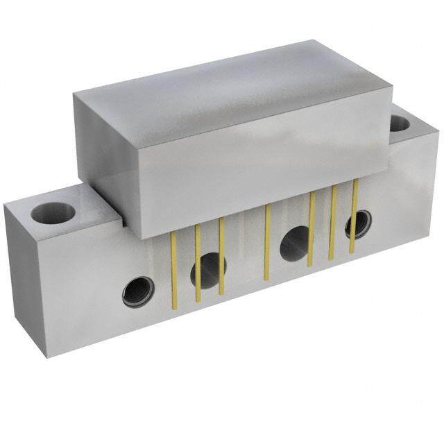
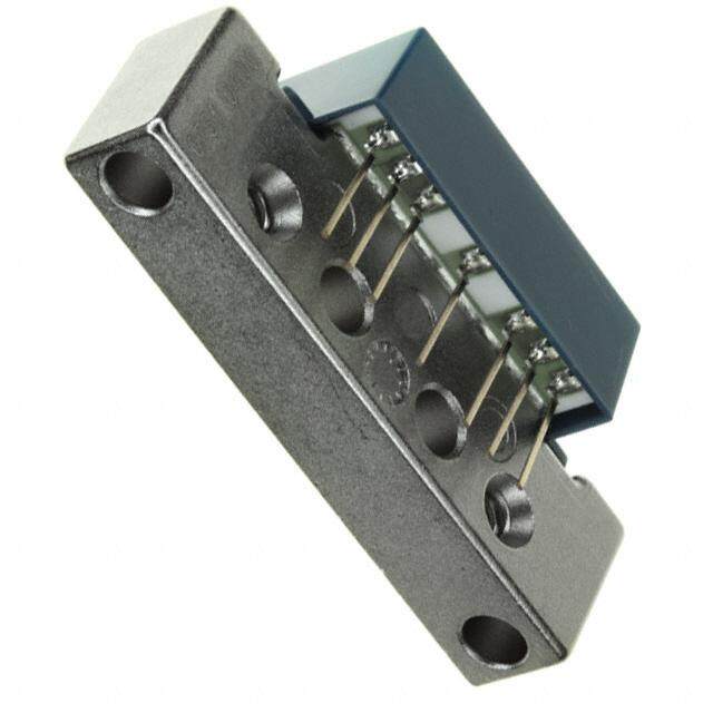
| 产品图片 |
|
| rohs | 否不符合限制有害物质指令(RoHS)规范要求 |
| 产品系列 | 放大器 IC,视频放大器,Analog Devices AD8013AR-14- |
| 数据手册 | |
| 产品型号 | AD8013AR-14 |
| 产品种类 | 视频放大器 |
| 供应商器件封装 | 14-SOICN |
| 其它名称 | AD8013AR14 |
| 包装 | 管件 |
| 压摆率 | 1000 V/µs |
| 双重电源电压 | +/- 2.1 V to +/- 6.5 V |
| 商标 | Analog Devices |
| 安装类型 | 表面贴装 |
| 安装风格 | SMD/SMT |
| 封装 | Tube |
| 封装/外壳 | 14-SOIC(0.154",3.90mm 宽) |
| 封装/箱体 | SOIC-14 |
| 工作温度范围 | - 40 C to + 85 C |
| 工作电源电压 | 4.2 V to 13 V |
| 工厂包装数量 | 56 |
| 带宽 | 140 MHz |
| 应用 | 电流反馈 |
| 放大器类型 | Current Feedback Amplifier |
| 最大功率耗散 | 1000 mW |
| 最大双重电源电压 | +/- 6.5 V |
| 最大工作温度 | + 85 C |
| 最小双重电源电压 | +/- 2.1 V |
| 最小工作温度 | - 40 C |
| 标准包装 | 56 |
| 电压-电源,单/双 (±) | 4.2 V ~ 13 V, ±2.1 V ~ 6.5 V |
| 电流-电源 | 3.5mA |
| 电流-输出/通道 | 30mA |
| 电源电压-最大 | 13 V |
| 电源电压-最小 | 4.2 V |
| 电源电流 | 3 mA, 3.5 mA |
| 电源类型 | Dual |
| 电路数 | 3 |
| 系列 | AD8013 |
| 输出类型 | - |
| 通道数量 | 3 Channel |


- 商务部:美国ITC正式对集成电路等产品启动337调查
- 曝三星4nm工艺存在良率问题 高通将骁龙8 Gen1或转产台积电
- 太阳诱电将投资9.5亿元在常州建新厂生产MLCC 预计2023年完工
- 英特尔发布欧洲新工厂建设计划 深化IDM 2.0 战略
- 台积电先进制程称霸业界 有大客户加持明年业绩稳了
- 达到5530亿美元!SIA预计今年全球半导体销售额将创下新高
- 英特尔拟将自动驾驶子公司Mobileye上市 估值或超500亿美元
- 三星加码芯片和SET,合并消费电子和移动部门,撤换高东真等 CEO
- 三星电子宣布重大人事变动 还合并消费电子和移动部门
- 海关总署:前11个月进口集成电路产品价值2.52万亿元 增长14.8%


PDF Datasheet 数据手册内容提取
a Single Supply, Low Power, Triple Video Amplifier AD8013 FEATURES PIN CONFIGURATION Three Video Amplifiers in One Package 14-Pin DIP & SOIC Package Drives Large Capacitive Load Excellent Video Specifications (R = 150 (cid:86)) L Gain Flatness 0.1 dB to 60 MHz DISABLE 1 1 14 OUT 2 0.02% Differential Gain Error DISABLE 2 2 13 –IN 2 0.06(cid:176) Differential Phase Error DISABLE 3 3 12 +IN 2 Low Power Operates on Single +5 V to +13 V Power Supplies +VS 4 AD8013 11 –VS +IN 1 5 10 +IN 3 4mA/Amplifier Max Power Supply Current High Speed –IN 1 6 9 –IN 3 140 MHz Unity Gain Bandwidth (3 dB) OUT 1 7 8 OUT 3 Fast Settling Time of 18ns (0.1%) 1000 V/(cid:109)s Slew Rate High Speed Disable Function per Channel Turn-Off Time 30 ns differential gain and phase error of 0.02% and 0.06(cid:176) . This Easy to Use makes the AD8013 ideal for broadcast and professional video 95 mA Short Circuit Current electronics. Output Swing to Within 1 V of Rails The AD8013 offers low power of 4mA per amplifier max and runs on a single +5 V to +13 V power supply. The outputs of APPLICATIONS each amplifier swing to within one volt of either supply rail to LCD Displays easily accommodate video signals. The AD8013 is unique Video Line Driver among current feedback op amps by virtue of its large capacitive Broadcast and Professional Video load drive. Each op amp is capable of driving large capacitive Computer Video Plug-In Boards loads while still achieving rapid settling time. For instance it Consumer Video can settle in 18 ns driving a resistive load, and achieves 40 ns RGB Amplifier in Component Systems (0.1%) settling while driving 200 pF. PRODUCT DESCRIPTION The outstanding bandwidth of 140 MHz along with 1000 V/m s The AD8013 is a low power, single supply, triple video of slew rate make the AD8013 useful in many general purpose amplifier. Each of the three amplifiers has 30 mA of output high speed applications where a single +5 V or dual power current, and is optimized for driving one back terminated video supplies up to – 6.5 V are required. Furthermore the AD8013’s load (150W ) each. Each amplifier is a current feedback amp- high speed disable function can be used to power down the lifier and features gain flatness of 0.1 dB to 60 MHz while offering amplifier or to put the output in a high impedance state. This can then be used in video multiplexing applications. The AD8013 is available in the industrial temperature range of 0.2 GRL = = + 1250W –40(cid:176) C to +85(cid:176) C. 0.1 B – d 0 500mV 500ns LIZED GAIN ––00..12 VS = +5V VS = – 5V 10900 A M R–0.3 O N –0.4 1 –0.5 0%0 5V 1M 10M 100M 1G FREQUENCY – Hz Fine-ScaleGainFlatnessvs.Frequency, G=+2,R =150W Channel Switching Characteristics for a 3:1 Mux L REV. A Information furnished by Analog Devices is believed to be accurate and © Analog Devices, Inc., 1995 reliable. However, no responsibility is assumed by Analog Devices for its use, nor for any infringements of patents or other rights of third parties which may result from its use. No license is granted by implication or One Technology Way, P.O. Box 9106, Norwood, MA 02062-9106, U.S.A. otherwise under any patent or patent rights of Analog Devices. Tel: 617/329-4700 Fax: 617/326-8703
AD8013–SPECIFICATIONS (@ T = +25(cid:56)C, R = 150 (cid:86), unless otherwise noted) A LOAD Model AD8013A Conditions V Min Typ Max Units S DYNAMIC PERFORMANCE Bandwidth (3 dB) No Peaking, G = +2 +5 V 100 125 MHz No Peaking, G = +2 – 5 V 110 140 MHz Bandwidth (0.1 dB) No Peaking, G = +2 +5 V 50 MHz No Peaking, G = +2 – 5 V 60 MHz Slew Rate 2 V Step +5 V 400 V/m s 6 V Step – 5 V 600 1000 V/m s Settling Time to 0.1% 0 V to +2 V – 5 V 18 ns 4.5 V Step, C = 200 pF – 6 V 40 ns LOAD R > 1 kW , R = 4 kW LOAD FB NOISE/HARMONIC PERFORMANCE Total Harmonic Distortion f = 5 MHz, R = 1 k – 5 V –76 dBc C L f = 5 MHz, R = 150 W – 5 V –66 dBc C L Input Voltage Noise f = 10 kHz +5 V, – 5 V 3.5 nV/(cid:214) Hz Input Current Noise f = 10 kHz (–I ) +5 V, – 5 V 12 pA/(cid:214) Hz IN Differential Gain (R = 150 W ) f = 3.58 MHz, G = +2 +5 V1 0.05 % L – 5 V 0.02 0.05 % Differential Phase (R = 150 W ) f = 3.58 MHz, G = +2 +5 V1 0.06 Degrees L – 5 V 0.06 0.12 Degrees DC PERFORMANCE Input Offset Voltage T to T +5 V, – 5 V 2 5 mV MIN MAX Offset Drift 7 m V/(cid:176) C Input Bias Current (–) +5 V, – 5 V 2 10 m A Input Bias Current (+) T to T +5 V, – 5 V 3 15 m A MIN MAX Open-Loop Transresistance +5 V 650 800 kW T to T 550 kW MIN MAX – 5 V 800 k 1.1 M W T to T 650 kW MIN MAX INPUT CHARACTERISTICS Input Resistance +Input – 5 V 200 kW –Input – 5 V 150 W Input Capacitance – 5 V 2 pF Input Common-Mode Voltage Range – 5 V 3.8 – V +5 V 1.2 3.8 +V Common-Mode Rejection Ratio Input Offset Voltage +5 V 52 56 dB Input Offset Voltage – 5 V 52 56 dB –Input Current +5 V, – 5 V 0.2 0.4 m A/V +Input Current +5 V, – 5 V 5 7 m A/V OUTPUT CHARACTERISTICS Output Voltage Swing R = 1 kW V –V 0.8 1.0 V L OL EE V –V 0.8 1.0 V CC OH R = 150 W V –V 1.1 1.3 V L OL EE V –V 1.1 1.3 V CC OH Output Current +5 V 30 mA – 5 V 25 30 mA Short-Circuit Current – 5 V 95 mA Capacitive Load Drive – 5 V 1000 pF MATCHING CHARACTERISTICS Dynamic Crosstalk G = +2, f = 5 MHz +5 V, – 5 V 70 dB Gain Flatness Match f = 20 MHz – 5 V 0.1 dB DC Input Offset Voltage +5 V, – 5 V 0.3 mV –Input Bias Current +5 V, – 5 V 1.0 m A –2– REV. A
AD8013 Model AD8013A Conditions V Min Typ Max Units S POWER SUPPLY Operating Range Single Supply +4.2 +13 V Dual Supply – 2.1 – 6.5 V Quiescent Current/Amplifier +5 V 3.0 3.5 mA – 5 V 3.4 4.0 mA – 6.5 V 3.5 mA Quiescent Current/Amplifier Power Down +5 V 0.25 0.35 mA – 5 V 0.3 0.4 mA Power Supply Rejection Ratio Input Offset Voltage V = – 2.5 V to – 5 V 70 76 dB S –Input Current +5 V, – 5 V 0.03 0.2 m A/V +Input Current +5 V, – 5 V 0.07 1.0 m A/V DISABLE CHARACTERISTICS Off Isolation f = 6 MHz +5 V, – 5 V –70 dB Off Output Impedance G = +1 +5 V, – 5 V 12 pF Turn-On Time 50 ns Turn-Off Time 30 ns Switching Threshold –V + xV 1.3 1.6 1.9 V S NOTES 1The test circuit for differential gain and phase measurements on a +5 V supply is ac coupled. Specifications subject to change without notice. ABSOLUTE MAXIMUM RATINGS1 Maximum Power Dissipation SupplyVoltage . . . . . . . . . . . . . . . . . . . . . . . . . . 13.2 V Total The maximum power that can be safely dissipated by the AD8013 InternalPowerDissipation2 is limited by the associated rise in junction temperature. The Plastic(N) . . . . . . . . .1.6Watts (Observe Derating Curves) maximum safe junction temperature for the plastic encapsulated SmallOutline(R) . . . .1.0Watts (Observe Derating Curves) parts is determined by the glass transition temperature of the Input Voltage (Common Mode) . . Lower of – V or – 12.25 V plastic, about 150(cid:176) C. Exceeding this limit temporarily may S DifferentialInputVoltage . . . . . . . . Output – 6V (Clamped) cause a shift in parametric performance due to a change in the Output Voltage Limit stresses exerted on the die by the package. Exceeding a junction Maximum . . . . . . . . . Lower of (+12 V from –V ) or (+V ) temperature of 175(cid:176) C for an extended period can result in S S Minimum . . . . . . . . .Higher of (–12.5 V from +V ) or (–V ) device failure. S S Output Short Circuit Duration While the AD8013 is internally short circuit protected, this may . . . . . . . . . . . . . . . . . . . .Observe Power Derating Curves not be enough to guarantee that the maximum junction temper- Storage Temperature Range ature is not exceeded under all conditions. To ensure proper N and R Package . . . . . . . . . . . . . . . . . . . –65(cid:176) C to +125(cid:176) C operation, it is important to observe the derating curves. Operating Temperature Range AD8013A . . . . . . . . . . . . . . . . . . . . . . . . . . –40(cid:176) C to +85(cid:176) C It must also be noted that in (noninverting) gain configurations Lead Temperature Range (Soldering10sec) . . . . . . . .+300(cid:176) C (with low values of gain resistor), a high level of input overdrive can result in a large input error current, which may result in a NOTES significant power dissipation in the input stage. This power 1Stresses above those listed under “Absolute Maximum Ratings” may cause must be included when computing the junction temperature rise permanent damage to the device. This is a stress rating only and functional operation of the device at these or any other conditions above those indicated in due to total internal power. the operational section of this specification is not implied. Exposure to absolute maximum rating conditions for extended periods may affect device reliability. 2.5 2Specification is for device in free air: TJ = +150(cid:176)C 14-Pin Plastic DIP Package: q JA = 75(cid:176)C/Watt atts 14-Pin SOIC Package: q = 120(cid:176)C/Watt W JA N – 2.0 ORDERING GUIDE ATIO 14-PIN DIP PACKAGE P SI S Temperature Package Package DI 1.5 R Model Range Description Options E W O AD8013AN –40(cid:176) C to +85(cid:176) C 14-Pin Plastic DIP N-14 M P 14-PIN SOIC AD8013AR-14 –40(cid:176) C to +85(cid:176) C 14-Pin Plastic SOIC R-14 MU 1.0 AD8013AR-14-REEL –40(cid:176) C to +85(cid:176) C 14-Pin Plastic SOIC R-14 AXI M AD8013AR-14-REEL7 –40(cid:176) C to +85(cid:176) C 14-Pin Plastic SOIC R-14 AD8013ACHIPS –40(cid:176) C to +85(cid:176) C Die Form 0.5 –50 –40–30–20 –10 0 10 20 30 40 50 60 70 80 90 AMBIENT TEMPERATURE – (cid:176)C Maximum Power Dissipation vs. Ambient Temperature REV. A –3–
AD8013 METALIZATION PHOTO Contact factory for latest dimensions. Dimensions shown in inches and (mm). +IN1 +vs DISABLE 3 5 4 3 –IN1 6 2 DISABLE 2 OUT1 7 1 DISABLE 1 0.044 (1.13) 14 OUT 2 OUT3 8 –IN3 9 10 11 12 13 +IN3 –VS +IN2 –IN2 0.071 (1.81) CAUTION ESD (electrostatic discharge) sensitive device. Electrostatic charges as high as 4000 V readily WARNING! accumulate on the human body and test equipment and can discharge without detection. Although the AD8013 features proprietary ESD protection circuitry, permanent damage may occur on devices subjected to high energy electrostatic discharges. Therefore, proper ESD precautions are recom- mended to avoid performance degradation or loss of functionality. ESD SENSITIVE DEVICE 6 12 s olt V5 p10 –E – V p- NO LOAD G – TAGE RAN43 GE SWING 86 RL = 150W OL TA V L E O OD2 T V 4 M U N- TP O U M1 O 2 M O C 0 0 1 2 3 4 5 6 7 1 2 3 4 5 6 7 SUPPLY VOLTAGE – – Volts SUPPLY VOLTAGE – – Volts Figure 1.Input Common-Mode Voltage Range vs. Figure 2.Output Voltage Swing vs. Supply Voltage Supply Voltage –4– REV. A
AD8013 10 3 p VS = – 5V 2 p- 8 V A WING – 6 ENT – µ 1 S R UTPUT VOLTAGE 42 VS = +5V INPUT BIAS CUR–01 –IB O –2 +IB 0 –3 10 100 1k 10k –60 –40 –20 0 20 40 60 80 100 120 140 LOAD RESISTANCE – W JUNCTION TEMPERATURE – (cid:176)C Figure 3.Output Voltage Swing vs. Load Resistance Figure 6.Input Bias Current vs. Junction Temperature 12 2 11 1 V VS = – 5V – m mA 10 GE 0 – A RRENT 9 T VOLT–1 Y CU VS = +5V FFSE VS = +5V SUPPL 8 NPUT O–2 VS = – 5V 7 I–3 6 –4 –60 –40 –20 0 20 40 60 80 100 120 140 –60 –40 –20 0 20 40 60 80 100 120 140 JUNCTION TEMPERATURE – (cid:176)C JUNCTION TEMPERATURE – (cid:176)C Figure 4.Total Supply Current vs. Junction Temperature Figure 7.Input Offset Voltage vs. Junction Temperature 11 140 VS = – 5V TA = +25(cid:176)C mA130 A10 – CURRENT – m 9 UIT CURRENT 120 SINK SOURCE LY RC100 SUPP 8 ORT CI H 90 S 7 80 1 2 3 4 5 6 7 –60 –40 –20 0 20 40 60 80 100 120 140 SUPPLY VOLTAGE – – Volts JUNCTION TEMPERATURE – (cid:176)C Figure 5.Supply Current vs. Supply Voltage Figure 8.Short Circuit Current vs. Junction Temperature REV. A –5–
AD8013 1k 70 W– G = +2 R R NCE 100 dB60 VCM R A – UT RESIST 10 EJECTION 50 R P OUTP 1 VS = – 5V MODE R40 SED-LOO0.1 OMMON-30 O C20 L C 0.01 10 100k 1M 10M 100M 1G 100k 1M 10M 100M 1G FREQUENCY – Hz FREQUENCY – Hz Figure 9.Closed-Loop Output Resistance vs. Figure 12.Common-Mode Rejection vs. Frequency Frequency 100k 80 VS = – 5V 70 B d 10k – 60 WNCE – CTION 50 A E UT RESIST 1k UPPLY REJ 3400 –PSR +PSR P S OUT 100 WER 20 O P 10 10 0 1M 10M 100M 1G 100k 1M 10M 100M 1G FREQUENCY – Hz FREQUENCY – Hz Figure 10.Output Resistance vs. Frequency, Disabled Figure 13.Power Supply Rejection Ratio vs. Frequency State 1k 1k 140 0 VRSL == –15kV –45 egrees 120 –90 – D (cid:214)V/Hz100 100(cid:214)A/Hz – dB –135HASE E n E p CE 100 –180P S S N GE NOI NONINVERTING I NT NOI MPEDA VOLTA 10 INVERTING I 10 CURRE TRANSI 80 60 VNOISE 1 1 40 100 1k 10k 100k 1M 10k 100k 1M 10M 100M 1G FREQUENCY – Hz FREQUENCY – Hz Figure 11.Input Current and Voltage Noise vs. Figure 14.Open-Loop Transimpedance vs. Frequency Frequency (Relative to 1 W ) –6– REV. A
AD8013 –30 G = +2 G = +1 es Bc ––4500 VVOS == –25VV p-p PHASE V SR L= =– 51V50W 0–90 – Degre N – d –60 +1 VS = +5V –180HIFT O S RTI –70 0 –270SE NIC DISTO ––8900 2RnLd = 150W OOP GAINZED) – dB––12 GAIN VS = – 5V PHA HARMO––110100 2RnLd = 1kW 3RrLd = 1kW CLOSED-L(NORMALI––34 VS = +5V –120 3rd –5 RL = 150W –6 1k 10k 100k 1M 10M 100M 1M 10M 100M 1G FREQUENCY – Hz FREQUENCY – Hz Figure 15.Harmonic Distortion vs. Frequency Figure 18.Closed-Loop Gain and Phase vs. Frequency, G = +1, R = 150W L 1800 2000 1600 VS = – 5V 1800 RL = 500W G = +10 1600 G = +10 1400 µs1200 µs1400 G = –1 E – V/1000 G = –1 E – V/1200 G = +2 W RAT 800 G = +2 W RAT1800000 SLE 600 G = +1 SLE 600 G = +1 400 400 200 200 1 2 3 4 5 6 7 8 1.5 2.5 3.5 4.5 5.5 6.5 7.5 OUTPUT STEP SIZE – V p-p SUPPLY VOLTAGE – – Volts Figure 16.Slew Rate vs. Output Step Size Figure 19.Maximum Slew Rate vs. Supply Voltage 2V 20ns 500mV 20ns 100 100 VIN 90 VIN 90 VOUT 10 VOUT 10 0% 0% 2V 500mV Figure 17.Large Signal Pulse Response, Gain = +1, Figure 20.Small Signal Pulse Response, Gain = +1, (R = 2 kW , R = 150 W , V = – 5 V) (R = 2 kW , R = 150 W , V = – 5 V) F L S F L S REV. A –7–
AD8013 50mV 20ns 2V 20ns 100 100 VIN 90 VIN 90 VOUT 10 VOUT 10 0% 0% 500mV 2V Figure 21.Large Signal Pulse Response, Gain = +10, Figure 24.Large Signal Pulse Response, Gain = –1, R = 301 W , R = 150 W , V = – 5 V) (R = 698 W , R = 150 W , V = – 5 V) F L S F L S +1 PHASE VS = +5V VS GR=L =– = 5+ V11500W 0––19800HIFT – Degrees +1 PHASE VS = +5V GR VL =S = =– 11 –550VW 901080 HIFT – Degrees CLOSED-LOOP GAIN(NORMALIZED) – dB––––01234 GAIN VS = – 5V VS = +5V –270PHASE S CLOSED-LOOP GAIN(NORMALIZED) – dB––––01234 GAIN VS = +5V VS = – 5V –90 PHASE S –5 –5 –6 –6 1M 10M 100M 1G 1M 10M 100M 1G FREQUENCY – Hz FREQUENCY – Hz Figure 22.Closed-Loop Gain and Phase vs. Frequency, Figure 25.Closed-Loop Gain and Phase vs. Frequency, G = +10, R = 150 W G = –1, R = 150 W L L 50mV 20ns 500mV 20ns 100 100 VIN 90 VIN 90 VOUT 10 VOUT 10 0% 0% 500mV 500mV Figure 23.Small Signal Pulse Response, Gain = +10, Figure 26.Small Signal Pulse Response, Gain = –1, (R = 301 W , R = 150 W , V = – 5 V) (R = 698 W , R = 150 W , V = – 5 V) F L S F L S –8– REV. A
AD8013 To estimate the –3 dB bandwidth for closed-loop gains of 2 or greater, for feedback resistors not listed in the following table, G = –10 es the following single pole model for the AD8013 may be used: PHASE RL = 150W 180 egre G VS = +5V VS = – 5V 90 FT – D ACL (cid:46) 1 +SCT (RF +Gnrin) +1 0 E SHI where: CT = transcapacitance (cid:62) 1 pF 0 –90 S R = feedback resistor GAIN– dB–1 GAIN PHA GF = ideal closed loop gain CLOSED-LOOP (NORMALIZED) –––234 VS = +5V VS = – 5V rGAinCn L== =i n(cid:230)Ł(cid:231) 1vcel+ortsRRiendGFg l(cid:246)ł(cid:247)ion o=ppu ntgo arieisnsei sgtaainnce (cid:62) 150 W –5 The –3 dB bandwidth is determined from this model as: –6 1M 10M 100M 1G 1 FREQUENCY – Hz f (cid:46) 3 2p C (R +Gnrin) T F Figure 27.Closed-Loop Gain and Phase vs. Frequency, This model will predict –3 dB bandwidth to within about 10% G = –10, RL = 150 W to 15% of the correct value when the load is 150 W and V = S – 5V. For lower supply voltages there will be a slight decrease in General bandwidth. The model is not accurate enough to predict either The AD8013 is a wide bandwidth, triple video amplifier that the phase behavior or the frequency response peaking of the offers a high level of performance on less than 4.0 mA per AD8013. amplifier of quiescent supply current. The AD8013 uses a It should be noted that the bandwidth is affected by attenuation proprietary enhancement of a conventional current feedback due to the finite input resistance. Also, the open-loop output architecture, and achieves bandwidth in excess of 200MHz with resistance of about 12 W reduces the bandwidth somewhat when low differential gain and phase errors, making it an extremely driving load resistors less than about 250 W . (Bandwidths will efficient video amplifier. be about 10% greater for load resistances above a few hundred The AD8013’s wide phase margin coupled with a high output ohms.) short circuit current make it an excellent choice when driving any capacitive load. High open-loop gain and low inverting Table I. –3 dB Bandwidth vs. Closed-Loop Gain and Feedback input bias current enable it to be used with large values of Resistor, R = 150 W (SOIC) L feedback resistor with very low closed-loop gain errors. V – Volts Gain R – Ohms BW – MHz S F It is designed to offer outstanding functionality and performance – 5 +1 2000 230 at closed-loop inverting or noninverting gains of one or greater. +2 845 (931) 150 (135) Choice of Feedback & Gain Resistors +10 301 80 –1 698 (825) 140 (130) Because it is a current feedback amplifier, the closed-loop band- –10 499 85 width of the AD8013 may be customized using different values +5 +1 2000 180 of the feedback resistor. Table I shows typical bandwidths at +2 887 (931) 120 (130) different supply voltages for some useful closed-loop gains when +10 301 75 driving a load of 150 W . –1 698 (825) 130 (120) The choice of feedback resistor is not critical unless it is –10 499 80 important to maintain the widest, flattest frequency response. Driving Capacitive Loads The resistors recommended in the table are those (chip When used in combination with the appropriate feedback resistors) that will result in the widest 0.1 dB bandwidth without resistor, the AD8013 will drive any load capacitance without peaking. In applications requiring the best control of bandwidth, oscillation. The general rule for current feedback amplifiers is 1% resistors are adequate. Package parasitics vary between the that the higher the load capacitance, the higher the feedback 14-pin plastic DIP and the 14-pin plastic SOIC, and may result resistor required for stable operation. Due to the high open-loop in a slight difference in the value of the feedback resistor used to transresistance and low inverting input current of the AD8013, achieve the optimum dynamic performance. Resistor values and the use of a large feedback resistor does not result in large closed- widest bandwidth figures are shown in parenthesis for the SOIC loop gain errors. Additionally, its high output short circuit current where they differ from those of the DIP. Wider bandwidths than makes possible rapid voltage slewing on large load capacitors. those in the table can be attained by reducing the magnitude of the feedback resistor (at the expense of increased peaking), For the best combination of wide bandwidth and clean pulse while peaking can be reduced by increasing the magnitude of response, a small output series resistor is also recommended. the feedback resistor. Table II contains values of feedback and series resistors which result in the best pulse responses. Figure 29 shows the AD8013 Increasing the feedback resistor is especially useful when driving driving a 300pF capacitor through a large voltage step with large capacitive loads as it will increase the phase margin of the virtually no overshoot. (In this case, the large and small signal closed-loop circuit. (Refer to the section on driving capacitive pulse responses are quite similar in appearance.) loads for more information.) REV. A –9–
AD8013 RF As noted in the warning under “Maximum Power Dissipation,” +VS 1.0µF a high level of input overdrive in a high noninverting gain circuit can result in a large current flow in the input stage. Though this 0.1µF RG current is internally limited to about 30 mA, its effect on the 4 15W total power dissipation may be significant. VIN AD801113 1.0µF RS CL VO High Performance Video Line Driver RT 0.1µF At a gain of +2, the AD8013 makes an excellent driver for a –VS back terminated 75 W video line (Figures 31, 32, and 33). Low differential gain and phase errors and wide 0.1 dB bandwidth Figure 28.Circuit for Driving a Capacitive Load can be realized. The low gain and group delay matching errors ensure excellent performance in RGB systems. Figures 34 and Table II. Recommended Feedback and Series Resistors vs. 35 show the worst case matching. Capacitive Load and Gain R – Ohms RG RF S CL – pF RF – Ohms G = 2 G ‡ 3 +VS 0.1µF 20 2k 25 15 75W 50 2k 25 15 75W 4 75W CABLE 100 3k 20 15 CABLE AD8013 VOUT 200 4k 15 15 VIN 11 0.1µF 75W 75W 300 6k 15 15 –VS ‡ 500 7k 15 15 Figure 31.A Video Line Driver Operating at a Gain of +2 (R = R from Table I) 500mV 50ns F G 100 VIN 90 GRL = = + 1250W 0 grees PHASE e D VS = – 5V –90 T – +1 VS = +5V –180HIF S E VOUT 01%0 1V OOP GAINZED) – dB––012 GAIN VS = – 5V –270PHAS FCiLg =u r3e0 209 p.FP,u Gls e= R+2e,s RpoF n=s 6ek D, RriSv =in 1g5 a W Large Load Capacitor. CLOSED-L(NORMALI––34 VS = +5V –5 Overload Recovery The three important overload conditions are: input common- –6 1M 10M 100M 1G mode voltage overdrive, output voltage overdrive, and input FREQUENCY – Hz current overdrive. When configured for a low closed-loop gain, the amplifier will quickly recover from an input common- Figure 32.Closed-Loop Gain & Phase vs. Frequency mode voltage overdrive; typically in under 25 ns. When con- for the Line Driver figured for a higher gain, and overloaded at the output, the recovery time will also be short. For example, in a gain of +10, G = +2 with 15% overdrive, the recovery time of the AD8013 is about RL = 150W 20 ns (see Figure 30). For higher overdrive, the response is +0.2 somewhat slower. For 6 dB overdrive, (in a gain of +10), the +0.1 recovery time is about 65 ns. B 0 d – N –0.1 500mV 50ns D GAI –0.2 VS = – 5V VIN19000 ALIZE –0.3 VS = +5V M R –0.4 O N –0.5 1M 10M 100M 1G VOUT 10 FREQUENCY – Hz 0% 5V Figure 33.Fine-Scale Gain Flatness vs. Frequency, G = +2, R = 150 W L Figure 30.15% Overload Recovery, G = +10 (R = 300 W , F R = 1 kW , V = – 5 V) L S –10– REV. A
AD8013 1.5 VI +5V 1.0 G = +2 8k RL = 150W B 0.5 TO DISABLE PIN d – 4k 10k G N 0 –5V TCHI VS = +5V VI HIGH => AMPLIFIER ENABLED MA–0.5 VI LOW => AMPLIFIER DISABLED AIN VS = – 5V G–1.0 Figure 36.Level Shifting to Drive Disable Pins on Dual Supplies –1.5 The AD8013’s input stages include protection from the large –2.0 differential input voltages that may be applied when disabled. 1M 10M 100M 1G Internal clamps limit this voltage to about – 3 V. The high input to FREQUENCY – Hz output isolation will be maintained for voltages below this limit. Figure 34.Closed-Loop Gain Matching vs. Frequency 3:1 Video Multiplexer Wiring the amplifier outputs together will form a 3:1 mux with 10 G = +2 excellent switching behavior. Figure 37 shows a recommended 8 RL = 150W configuration which results in –0.1 dB bandwidth of 35 MHz 6 and OFF channel isolation of 60 dB at 10 MHz on – 5 V 4 VS = +5V supplies. The time to switch between channels is about 50 ns. s n LAY – 2 VS = – 5V DELAY Switching time is virtually unaffected by signal level. DE 1.0 665W 845W GROUP 0.5 GRL = = + 1250W VS = – 5V +VS 0 6 4 84W –0.5 DELAY VS = +5V 7 –1.0 MATCHING VIN1 75W 5 1 100k 1M 10M 100M FREQUENCY – Hz DISABLE 1 Figure 35.Group Delay and Group Delay Matching 665W 845W vs. Frequency, G = +2, RL = 150 W 75W 13 84W CABLE 14 VOUT Disable Mode Operation VIN2 12 2 75W Pulling the voltage on any one of the Disable pins about 1.6V 75W up from the negative supply will put the corresponding amplifier into a disabled, powered down, state. In this DISABLE 2 665W 845W condition, the amplifier’s quiescent current drops to about 0.3 mA, its output becomes a high impedance, and there is a high level of isolation from input to output. In the case of 9 84W 8 the gain of two line driver for example, the impedance at the 11 output node will be about the same as for a 1.6 kW resistor VIN3 75W 10 3 (the feedback plus gain resistors) in parallel with a 12 pF –VS capacitor and the input to output isolation will be about DISABLE 3 66 dB at 5 MHz. Figure 37.A Fast Switching 3:1 Video Mux (Supply Leaving the Disable pin disconnected (floating) will leave Bypassing Not Shown) the corresponding amplifier operational, in the enabled state. The input impedance of the disable pin is about 40 kW in parallel with a few picofarads. When driven to 0 V, with 500mV 200ns the negative supply at –5 V, about 100 m A flows into the 100 90 disable pin. When the disable pins are driven by complementary output CMOS logic, on a single 5 V supply, the disable and enable times are about 50 ns. When operated on dual supplies, level shifting will be required from standard logic outputs to 10 0% the Disable pins. Figure 36 shows one possible method 5V which results in a negligible increase in switching time. Figure 38.Channel Switching Characteristic for the 3:1 Mux REV. A –11–
AD8013 2:1 Video Multiplexer The AD8013 can be used to build a circuit for switching between Configuring two amplifiers as unity gain followers and using the any two arbitrary gains while maintaining a constant input third to set the gain results in a high performance 2:1 mux impedance. The example of Figure 41 shows a circuit for switching (Figures 39 and 40). This circuit takes advantage of the very low between a noninverting gain of 1 and an inverting gain of 1. The crosstalk between Channels 2 and 3 to achieve the OFF channel total time for channel switching and output voltage settling is isolation shown in Figure 40. This circuit can achieve about 80ns. differential gain and phase of 0.03% and 0.07(cid:176) respectively. 698W 698W 95 0/ +5V 1 13 R2k1W 2k 6 4 18– – 2 14 13 5 1 7 84 VVIINNBA 1120 32DISA8BLE R1R10034WW 65 1 R75 VOUT VIN 5100W0W 12 141k 10 DDIISS3 31 15W VOUT C20 9 3 R2k2W 845W 1k 9 118 R6 DISABLE 845W –5V 845W 845W Figure 39.2:1 Mux with High Isolation and Low Differential Gain and Phase Errors Figure 41. Circuit to Switch Between Gains of –1 and +1 2 1 GAIN 500mV 500mV 200ns 0 B 100 – d –1 90 N AI –2 G OP –3 –30 CLOSED-LO –––456 FEEDTHROUGH –––456000 HROUGH – dB 01%0 5V T D –7 –70 E E F –8 –80 Figure 42.Switching Characteristic for Circuit of Figure 41 1M 10M 100M 1G FREQUENCY – Hz Figure 40.2:1 Mux ON Channel Gain and Mux OFF Channel Feedthrough vs. Frequency Gain Switching OUTLINE DIMENSIONS Dimensions shown in inches and (mm). 14-Lead Plastic DIP (N-14) 14-Lead SOIC (R-14) A. 0.795 (20.19) 0.3444 (8.75) U.S. 0.725 (18.42) 0.3367 (8.55) N 14 8 0.280 (7.11) 0.1574 (4.00) 14 8 0.2440 (6.20) ED I 0.240 (6.10) T 1 7 0.1497 (3.80) 1 7 0.2284 (5.80) N 0.325 (8.25) RI 0.060 (1.52) 0.300 (7.62)0.195 (4.95) P 0.210 (5.33) PIN 1 0.015 (0.38) 0.115 (2.93) 0.0098 (0.25) PIN 1 00..00658382 ((11..7355)) 00..00109969 ((00..5205))x 45(cid:176) MAX 0.130 0.0040 (0.10) 0.160 (4.06) (3.30) 0.115 (2.9300)..002124 ((00..535586)) (02.1.5040) 00..007405 ((11..7175)) SPMELIAANNTIENG 00..001058 ((00..328014)) SEPALTAINNGE 0(B1.0.S25C70)0 00..00119328 ((00..4395)) 00..00009785 ((00..2159)) 80(cid:176)(cid:176) 00..00510600 ((10..2471)) BSC –12– REV. A