ICGOO在线商城 > 集成电路(IC) > 线性 - 放大器 - 视频放大器和频缓冲器 > AD810ARZ-REEL7
 Datasheet下载
- 型号: AD810ARZ-REEL7
- 制造商: Analog
- 库位|库存: xxxx|xxxx
- 要求:
| 数量阶梯 | 香港交货 | 国内含税 |
| +xxxx | $xxxx | ¥xxxx |
查看当月历史价格
查看今年历史价格
AD810ARZ-REEL7产品简介:
ICGOO电子元器件商城为您提供AD810ARZ-REEL7由Analog设计生产,在icgoo商城现货销售,并且可以通过原厂、代理商等渠道进行代购。 AD810ARZ-REEL7价格参考。AnalogAD810ARZ-REEL7封装/规格:线性 - 放大器 - 视频放大器和频缓冲器, Video Amp, 1 Current Feedback 8-SOIC。您可以下载AD810ARZ-REEL7参考资料、Datasheet数据手册功能说明书,资料中有AD810ARZ-REEL7 详细功能的应用电路图电压和使用方法及教程。
AD810ARZ-REEL7是Analog Devices Inc.生产的一款高速视频放大器,属于线性放大器中的视频放大器和缓冲器类别。该器件具有宽达140 MHz的带宽,支持RGB视频信号处理,适用于需要高质量模拟视频信号传输的应用场景。

典型应用场景包括:高性能视频显示系统,如专业监视器、医疗成像设备、工业视觉系统和广播级视频设备;RGB信号驱动电路中,用于增强信号驱动能力,确保长距离传输时的信号完整性;在视频信号分配器、切换器和矩阵系统中作为缓冲放大器使用,有效隔离前后级电路,减少信号干扰与失真。

AD810ARZ-REEL7采用8引脚SOIC封装,具备低功耗、高转换速率(约550 V/μs)和优异的差分增益/相位性能,可支持NTSC、PAL、SECAM等多种视频标准,确保色彩还原准确。其工作电压为±5V至±6V双电源供电,也可单电源工作,灵活性高。

此外,该器件具有良好的输出驱动能力,可驱动75Ω负载,适合直接连接视频电缆。因其高稳定性和抗干扰能力,广泛应用于对图像质量要求较高的工业、医疗及通信设备中。REEL7后缀表示产品以卷带包装形式供应,适用于自动化贴片生产线,适合大规模制造使用。
| 参数 | 数值 |
| -3db带宽 | 80MHz |
| 产品目录 | 集成电路 (IC) |
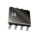
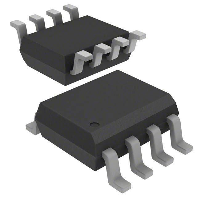
| 描述 | IC OPAMP VIDEO LOW POWER 8SOIC |
| 产品分类 | |
| 品牌 | Analog Devices Inc |
| 数据手册 | |
| 产品图片 |
|
| 产品型号 | AD810ARZ-REEL7 |
| rohs | 无铅 / 符合限制有害物质指令(RoHS)规范要求 |
| 产品系列 | - |
| 供应商器件封装 | 8-SOIC |
| 包装 | Digi-Reel® |
| 压摆率 | 1000 V/µs |
| 安装类型 | 表面贴装 |
| 封装/外壳 | 8-SOIC(0.154",3.90mm 宽) |
| 应用 | 电流反馈 |
| 标准包装 | 1 |
| 电压-电源,单/双 (±) | 5 V ~ 36 V, ±2.5 V ~ 18 V |
| 电流-电源 | 6.8mA |
| 电流-输出/通道 | 60mA |
| 电路数 | 1 |
| 输出类型 | - |


- 商务部:美国ITC正式对集成电路等产品启动337调查
- 曝三星4nm工艺存在良率问题 高通将骁龙8 Gen1或转产台积电
- 太阳诱电将投资9.5亿元在常州建新厂生产MLCC 预计2023年完工
- 英特尔发布欧洲新工厂建设计划 深化IDM 2.0 战略
- 台积电先进制程称霸业界 有大客户加持明年业绩稳了
- 达到5530亿美元!SIA预计今年全球半导体销售额将创下新高
- 英特尔拟将自动驾驶子公司Mobileye上市 估值或超500亿美元
- 三星加码芯片和SET,合并消费电子和移动部门,撤换高东真等 CEO
- 三星电子宣布重大人事变动 还合并消费电子和移动部门
- 海关总署:前11个月进口集成电路产品价值2.52万亿元 增长14.8%


PDF Datasheet 数据手册内容提取
a Low Power Video Op Amp with Disable AD810 FEATURES CONNECTION DIAGRAM High Speed 8-Pin Plastic Mini-DIP (N), SOIC (R) 80 MHz Bandwidth (3 dB, G = +1) and Cerdip (Q) Packages 75 MHz Bandwidth (3 dB, G = +2) 1000 V/(cid:109)s Slew Rate OFFSET 50 ns Settling Time to 0.1% (V = 10 V Step) NULL 1 AD810 8 DISABLE O Ideal for Video Applications –IN 2 7 +VS 30 MHz Bandwidth (0.1 dB, G = +2) +IN 3 6 OUTPUT 0.02% Differential Gain 0.04(cid:56) Differential Phase –VS 4 TOP VIEW 5 ONUFFLSLET Low Noise 2.9 nV/(cid:214) Hz Input Voltage Noise PRODUCT DESCRIPTION 13 pA/(cid:214) Hz Inverting Input Current Noise The AD810 is a composite and HDTV compatible, current Low Power feedback, video operational amplifier, ideal for use in systems 8.0 mA Supply Current max such as multimedia, digital tape recorders and video cameras. 2.1 mA Supply Current (Power-Down Mode) The 0.1 dB flatness specification at bandwidth of 30 MHz High Performance Disable Function (G = +2) and the differential gain and phase of 0.02% and Turn-Off Time 100 ns 0.04(cid:176) (NTSC) make the AD810 ideal for any broadcast quality Break Before Make Guaranteed video system. All these specifications are under load conditions Input to Output Isolation of 64 dB (OFF State) of 150 W (one 75 W back terminated cable). Flexible Operation Specified for (cid:54)5 V and (cid:54)15 V Operation The AD810 is ideal for power sensitive applications such as (cid:54)2.9 V Output Swing Into a 150 (cid:86) Load (V = (cid:54)5 V) video cameras, offering a low power supply current of 8.0 mA S max. The disable feature reduces the power supply current to APPLICATIONS only 2.1 mA, while the amplifier is not in use, to conserve Professional Video Cameras power. Furthermore the AD810 is specified over a power supply Multimedia Systems range of – 5 V to – 15 V. NTSC, PAL & SECAM Compatible Systems The AD810 works well as an ADC or DAC buffer in video Video Line Driver systems due to its unity gain bandwidth of 80 MHz. Because the ADC/DAC Buffer AD810 is a transimpedance amplifier, this bandwidth can be DC Restoration Circuits maintained over a wide range of gains while featuring a low noise of 2.9 nV/(cid:214) Hz for wide dynamic range applications. 0.10 0.20 0 0.09 GAIN = +2 0.18 dB– N 01 PGHAAISNE RGLA =IN 1 =5V± 0+5SW2V = ±15V ––––1149385050seegre DT –FHI SSEA % N –AIGL IANTER 0000....00006578 GAIN RRf1MC0FLO 0 ===D I 3RU71.155EL508AWWMTHEzD RAMP 0000....11116420 esreegD – SEAPHL A AIGP O––21 ±2.5V ––222750PH EFIFD 00..0034 PHASE 00..0086 TIENRE LOD-–3 VS = ±15V 0.02 0.04 FFDI EOS–4 ±5V 0.01 0.02 LC ±2.5V –5 0 0 1 10 100 1000 5 6 7 8 9 10 11 12 13 14 15 FREQUENCY – MHz SUPPLY VOLTAGE – ± Volts Closed-Loop Gain and Phase vs. Frequency, G = +2, Differential Gain and Phase vs. Supply Voltage R = 150, R = 715 W L F REV.A Information furnished by Analog Devices is believed to be accurate and reliable. However, no responsibility is assumed by Analog Devices for its use, nor for any infringements of patents or other rights of third parties which may result from its use. No license is granted by implication or One Technology Way, P.O. Box 9106, Norwood, MA 02062-9106, U.S.A. otherwise under any patent or patent rights of Analog Devices. Tel: 617/329-4700 Fax: 617/326-8703
AD810–SPECIFICATIONS (@ T = +25(cid:56)C and V = (cid:54)15 V dc, R = 150 (cid:86) unless otherwise noted) A S L AD810A AD810S1 Parameter Conditions V Min Typ Max Min Typ Max Units S DYNAMIC PERFORMANCE 3 dB Bandwidth (G = +2) R = 715 – 5 V 40 50 40 50 MHz FB (G = +2) R = 715 – 15 V 55 75 55 75 MHz FB (G = +1) R = 1000 – 15 V 40 80 40 80 MHz FB (G = +10) R = 270 – 15 V 50 65 50 65 MHz FB 0.1 dB Bandwidth (G = +2) R = 715 – 5 V 13 22 13 22 MHz FB (G = +2) R = 715 – 15 V 15 30 15 30 MHz FB Full Power Bandwidth V = 20 V p-p, O R = 400 W – 15 V 16 16 MHz L Slew Rate2 R = 150 W – 5 V 350 350 V/m s L R = 400 W – 15 V 1000 1000 V/m s L Settling Time to 0.1% 10 V Step, G = –1 – 15 V 50 50 ns Settling Time to 0.01% 10 V Step, G = –1 – 15 V 125 125 ns Differential Gain f = 3.58 MHz – 15 V 0.02 0.05 0.02 0.05 % f - 3.58 MHz – 5 V 0.04 0.07 0.04 0.07 % Differential Phase f = 3.58 MHz – 15 V 0.04 0.07 0.04 0.07 Degrees f = 3.58 MHz – 5 V 0.045 0.08 0.045 0.08 Degrees Total Harmonic Distortion f = 10 MHz, V = 2 V p-p O R = 400 W , G = +2 – 15 V –61 –61 dBc L INPUT OFFSET VOLTAGE – 5 V, – 15 V 1.5 6 1.5 6 mV T –T – 5 V, – 15 V 2 7.5 4 15 mV MIN MAX Offset Voltage Drift 7 15 m V/(cid:176) C INPUT BIAS CURRENT –Input T –T – 5 V, – 15 V 0.7 5 0.8 5 m A MIN MAX +Input T –T – 5 V, – 15 V 2 7.5 2 10 m A MIN MAX OPEN-LOOP T –T MIN MAX TRANSRESISTANCE V = – 10 V, R = 400 W – 15 V 1.0 3.5 1.0 3.5 MW O L V = – 2.5 V, R = 100 W – 5 V 0.3 1.2 0.2 1.0 MW O L OPEN-LOOP T –T MIN MAX DC VOLTAGE GAIN V = – 10 V, R = 400 W – 15 V 86 100 80 100 dB O L V = – 2.5 V, R = 100 W – 5 V 76 88 72 88 dB O L COMMON-MODE REJECTION T –T MIN MAX V V = – 12 V – 15 V 56 64 56 64 dB OS CM V = – 2.5 V – 5 V 52 60 50 60 dB CM – Input Current T –T – 5 V, – 15 V 0.1 0.4 0.1 0.4 m A/V MIN MAX POWER SUPPLY REJECTION – 4.5 V to – 18 V V T –T 65 72 60 72 dB OS MIN MAX – Input Current T –T 0.05 0.3 0.05 0.3 m A/V MIN MAX INPUT VOLTAGE NOISE f = 1 kHz – 5 V, – 15 V 2.9 2.9 nV/(cid:214) Hz INPUT CURRENT NOISE –I , f = 1 kHz – 5 V, – 15 V 13 13 pA/(cid:214) Hz IN +I , f = 1 kHz – 5 V, – 15 V 1.5 1.5 pA/(cid:214) Hz IN INPUT COMMON-MODE – 5 V – 2.5 – 3.0 – 2.5 – 3 V VOLTAGE RANGE – 15 V – 12 – 13 – 12 – 13 V OUTPUT CHARACTERISTICS Output Voltage Swing3 R = 150 W , T –T – 5 V – 2.5 – 2.9 – 2.5 – 2.9 V L MIN MAX R = 400 W – 15 V – 12.5 – 12.9 – 12.5 – 12.9 V L R = 400 W , T –T – 15 V – 12 – 12 V L MIN MAX Short-Circuit Current – 15 V 150 150 mA Output Current T –T – 5 V, – 15 V 40 60 30 60 mA MIN MAX OUTPUT RESISTANCE Open Loop (5 MHz) 15 15 W INPUT CHARACTERISTICS Input Resistance +Input – 15 V 2.5 10 2.5 10 MW –Input – 15 V 40 40 W Input Capacitance +Input – 15 V 2 2 pF DISABLE CHARACTERISTICS4 OFF Isolation f = 5 MHz, See Figure 43 64 64 dB OFF Output Impedance See Figure 43 (R + R )(cid:105)13 pF (R + R )(cid:105)13 pF F G F G –2– REV. A
AD810 AD810A AD810S1 Parameter Conditions V Min Typ Max Min Typ Max Units S Turn On Time5 Z = Low, See Figure 54 170 170 ns OUT Turn Off Time Z = High 100 100 ns OUT Disable Pin Current Disable Pin = 0 V – 5 V 50 75 50 75 m A – 15 V 290 400 290 400 m A Min Disable Pin Current to Disable T –T – 5 V, – 15 V 30 30 m A MIN MAX POWER SUPPLY Operating Range +25(cid:176) C to T – 2.5 – 18 – 2.5 – 18 V MAX T – 3.0 – 18 – 3.5 – 18 V MIN Quiescent Current – 5 V 6.7 7.5 6.7 7.5 mA – 15 V 6.8 8.0 6.8 8.0 mA T –T – 5 V, – 15 V 8.3 10.0 9 11.0 mA MIN MAX Power-Down Current – 5 V 1.8 2.3 1.8 2.3 mA – 15 V 2.1 2.8 2.1 2.8 mA NOTES 1See Analog Devices Military Data Sheet for 883B Specifications. 2Slew rate measurement is based on 10% to 90% rise time with the amplifier configured for a gain of –10. 3Voltage Swing is defined as useful operating range, not the saturation range. 4Disable guaranteed break before make. 5Turn On Time is defined with – 5 V supplies using complementary output CMOS to drive the disable pin. Specifications subject to change without notice. ABSOLUTE MAXIMUM RATINGS1 MAXIMUM POWER DISSIPATION Supply Voltage . . . . . . . . . . . . . . . . . . . . . . . . . . . . . . . .– 18 V The maximum power that can be safely dissipated by the Internal Power Dissipation2 . . . . . . . Observe Derating Curves AD810 is limited by the associated rise in junction temperature. Output Short Circuit Duration . . . . Observe Derating Curves For the plastic packages, the maximum safe junction tempera- Common-Mode Input Voltage . . . . . . . . . . . . . . . . . . . . . .– V ture is 145(cid:176) C. For the cerdip package, the maximum junction S Differential Input Voltage . . . . . . . . . . . . . . . . . . . . . . . .– 6 V temperature is 175(cid:176) C. If these maximums are exceeded momen- Storage Temperature Range tarily, proper circuit operation will be restored as soon as the die Plastic DIP . . . . . . . . . . . . . . . . . . . . . . . . –65(cid:176) C to +125(cid:176) C temperature is reduced. Leaving the device in the “overheated” Cerdip . . . . . . . . . . . . . . . . . . . . . . . . . . . –65(cid:176) C to +150(cid:176) C condition for an extended period can result in device burnout. Small Outline IC . . . . . . . . . . . . . . . . . . . –65(cid:176) C to +125(cid:176) C To ensure proper operation, it is important to observe the Operating Temperature Range derating curves. AD810A . . . . . . . . . . . . . . . . . . . . . . . . . . . –40(cid:176) C to +85(cid:176) C AD810S . . . . . . . . . . . . . . . . . . . . . . . . . . –55(cid:176) C to +125(cid:176) C 2.4 2.2 NLOeaTdE STemperature Range (Soldering 60 sec) . . . . . . . +300(cid:176) C ERsattW12..80 8M-IPNIIN-D IP 1Stresses above those listed under “Absolute Maximum Ratings” may cause WO– N 1.6 PO1.4 poomppeareexmrriaamattniiuooemnnn aot l rf ad tsrhaeinmcet gdia oegcnvoei ncotdeof i a tttitoh htnhiesse sdsfeope ovre ircec iaxefnit.c eyanT otdihtoehinsde rpii scse oranni oodsdtit tsri ieommsnspas y lrai aebatdfoifn.ve gecE ttx ohdpnoeolsvysei uc iarnene dr dietc loaifa utbaendbicls ititoinyol .utnhtaeel ALTTOATIPSIISD011...820 8S-OPIINC 8C-EPRINDIP 8M-IPNIIN-DIP 28-Pin Plastic Package: q = 90(cid:176)C/Watt; 8-Pin Cerdip Package: q = 110(cid:176)C/Watt; 0.6 8-Pin SOIC Package: q JJAA = 150(cid:176)C/Watt. JA 0.4–60 –40 –20 0 20 40 60 80 100 120 140 AMBIENT TEMPERATURE – °C ESD SUSCEPTIBILITY ESD (electrostatic discharge) sensitive device. Electrostatic Maximum Power Dissipation vs. Temperature charges as high as 4000 volts, which readily accumulate on the human body and on test equipment, can discharge without While the AD810 is internally short circuit protected, this may detection. Although the AD810 features ESD protection not be sufficient to guarantee that the maximum junction circuitry, permanent damage may still occur on these devices if temperature is not exceeded under all conditions. they are subjected to high energy electrostatic discharges. Therefore, proper ESD precautions are recommended to avoid 0.1µF +VS SEE TEXT 10kW any performance degradation or loss of functionality. 7 1 ORDERING GUIDE 2 5 AD810 6 Temperature Package Package 3 4 0.1µF Model Range Description Option AD810AN –40(cid:176) C to +85(cid:176) C 8-Pin Plastic DIP N-8 –VS AD810AR –40(cid:176) C to +85(cid:176) C 8-Pin Plastic SOIC R-8 Offset Null Configuration AD810AR-REEL –40(cid:176) C to +85(cid:176) C 8-Pin Plastic SOIC R-8 5962-9313201MPA –55(cid:176) C to +125(cid:176) C 8-Pin Cerdip Q-8 REV. A –3–
AD810–Typical Characteristics solt±V– E GTALVOT UTPU OHETF ODEUITGNAM21105500 NO R LLO =A 1D50W solt±V– E GTALVOT UTPU OHETF ODEUITGNAM21105500 NO R LLO =A 1D50W 0 5 10 15 20 0 5 10 15 20 SUPPLY VOLTAGE – ±Volts SUPPLY VOLTAGE – ±Volts Figure 1.Input Common-Mode Voltage Range vs. Figure 2.Output Voltage Swing vs. Supply Supply Voltage 35 10 30 9 pp-ts ol VE –G 2205 ±15V SUPPLY Am– T ENR 8 VS = ±15V VS = ±5V AT UR 7 L C O VT 15 Y PL U P 6 PT10 US U O ±5V SUPPLY 5 5 0 4 10 100 1k 10k –60 –40 –20 0 20 40 60 80 100 120 140 LOAD RESISTANCE – Ohms JUNCTION TEMPERATURE – °C Figure 3.Output Voltage Swing vs. Load Resistance Figure 4.Supply Current vs. Junction Temperature 10 10 8 8 6 V 6 Aµ – NT 4 NVSO N= I±N5VVE, R±T15INVG INPUT m– E AG 4 VS = ±5V E 2 T 2 R L R O UCS IAB –02 VT SEFF –20 VS = ±15V UTP –4 INVERTING INPUT OT U –4 IN –6 VS = ±5V, ±15V NPI –6 –8 –8 –10 –10 –60 –40 –20 0 20 40 60 80 100 120 140 –60 –40 –20 0 20 40 60 80 100 120 140 JUNCTION TEMPERATURE – °C JUNCTION TEMPERATURE – °C Figure 5.Input Bias Current vs. Temperature Figure 6.Input Offset Voltage vs. Junction Temperature –4– REV. A
Typical Characteristics–AD810 250 120 Am 100 – T NRER 200 VS = ±15V Am – NT 80 VS = ± 15V U E C R T UICIRC 150 RUCT PU 60 RTOHS 100 TOU 40 VS = ± 5V VS = ±5V 50 20 –60 –40 –20 0 +20 +40 +60 +80 +100 +120 +140 –60 –40 –20 0 +20 +40 +60 +80 +100 +120 +140 JUNCTION TEMPERATURE – °C JUNCTION TEMPERATURE – °C Figure 7.Short Circuit Current vs. Temperature Figure 8.Linear Output Current vs. Temperature 10.0 1M W– E CN GAIN = 2 VS = ±5V ASTSIRET U 1.0 RF = 715W W– E CANTS 100k TPUOOP O 0.1 VS = ±15V IESRT PUT 10k L U D- O 1k E S O L C 0.01 100 10k 100k 1M 10M 100M 100k 1M 10M 100M FREQUENCY – Hz FREQUENCY – Hz Figure 9.Closed-Loop Output Resistance vs. Frequency Figure 10.Output Resistance vs. Frequency, Disabled State 30 100 100 VS = ±15V VS = ±5V TO ±15V 25 pp-s olt V –GEALTO VUTPUT 112500 ± ORLU T= P4U00TW LEVEL F OVRS =3 %±5 TVHD zH/ nV– E ISNOE GALTOV10 VICNOUVLRETRRAETGNIENT GN N OIONISIPSEUET 10z H/ pA– E ISNOT NRERU O C NONINVERTING INPUT 5 CURRENT NOISE 1 1 0 100k 1M 10M 100M 10 100 1k 10k 100k FREQUENCY – Hz FREQUENCY – Hz Figure 11.Large Signal Frequency Response Figure 12.Input Voltage and Current Noise vs. Frequency REV. A –5–
AD810–Typical Characteristics 100 80 90 70 RF = 715W Bd Bd AV = +2 N – 80 – N 60 O O TICE 70 ICTE 50 VS = ±15V JE EJ RE 60 RY 40 VS = ±5V D L O P -MN 50 PSU 30 OMM 40 R EW 20 CURVES ARE FOR WORST CASE O O CONDITION WHERE ONE SUPPLY C P IS VARIED WHILE THE OTHER IS 30 10 HELD CONSTANT 20 10k 100k 1M 10M 100M 10k 100k 1M 10M 100M FREQUENCY – Hz FREQUENCY – Hz Figure 13.Common-Mode Rejection vs. Frequency Figure 14.Power Supply Rejection vs. Frequency –40 –40 VO = 2V p-p ±15V SUPPLIES Bcd– N –60 RGLA =IN 1 =0 0+W2 VS = ±5V cB dN – –60 RGLA =IN 4 =0 0+W2 O O IRT 2nd HARMONIC TIR –80 OSTDI –80 3rd HARMONIC TOSDI VOUT = 20V p-p C NIOMARH –100 2nd VS = ±15V C NIMORAH––112000 32rndd H HAARRMMOONNICIC VOUT = 2V p-p 2nd 3rd –120 3rd –140 100 1k 10k 100k 1M 10M 100 1k 10k 100k 1M 10M FREQUENCY – Hz FREQUENCY – Hz Figure 15.Harmonic Distortion vs. Frequency (R = 100 W ) Figure 16.Harmonic Distortion vs. Frequency (R = 400 W ) L L 10 1200 8 V0 6 0.01% 1000 RL = 400W O TV ±OMRFG 204 0.1% RF = RG = 1kW µsV/– E AT 800 GAIN = –10 GAIN = +10 INW –2 RL = 400W RW 600 S E T U –4 0.1% 0.01% SL P T GAIN = +2 UO –6 400 –8 –10 200 0 20 40 60 80 100 120 140 160 180 200 2 4 6 8 10 12 14 16 18 SETTLING TIME – ns SUPPLY VOLTAGE – ±Volts Figure 17.Output Swing and Error vs. Settling Time Figure 18.Slew Rate vs. Supply Voltage –6– REV. A
Typical Characteristics, Noninverting Connection–AD810 RF 1V 20nS 100 +VS 0.1µF VIN 90 VO TO TEKTRONIX RG 7 P6201 FET 2 PROBE AD810 6 VO VO VIN 33 4 0.1µF RL HPUP8L1S3E0 50W 100% GENERATOR –VS 1V Figure 19.Noninverting Amplifier Connection Figure 20.Small Signal Pulse Response, Gain = +1, R = 1 kW , R = 150 W , V = – 15 V F L S 0 0 GAIN = +1 PHASE RL = 150W ––4950 segreeD PHASE GRLA I=N 1 =k W+1 ––4950 seegrDe B d –INGAP OO-LEDSLOC ––––034121 GAIN VS = ±± 21±.555VVV V ±±S25 .V=5 V± 15V ––––112238275050 T –FHI SSEAPH Bd – INGAP OO-LEDSLOC––––034121 GAIN VS = ±± 2±1.555VVV ±±V25S.V5 =V ± 15V ––––112238275050 – T FHIE SSAPH –5 –5 1 10 100 1000 1 10 100 1000 FREQUENCY – MHz FREQUENCY – MHz Figure 21.Closed-Loop Gain and Phase vs. Frequency, Figure 22.Closed-Loop Gain and Phase vs. Frequency, G= +1. R = 1 kW for – 15 V, 910 W for – 5 V and – 2.5 V G= +1, R = 1 kW for – 15 V, 910 W for – 5 V and – 2.5 V F F 110 200 100 G = +1 180 G = +1 zMH– H TIDWNDA BdB3– 475896000000 RVOL == 125500WmV p-p R FR =F =7 510kWW P PEEAAKKININGG £ £0 .11d dBB zMH– H TIDWNDA BdB3– 1111682046000000 RVROLF === 127k55W00mW V p-p RF = 1kWPEAKING £ P 1EdABKING £ 0.1dB 30 40 20 RF = 1.5kW 20 RF = 1.5kW 2 4 6 8 10 12 14 16 18 2 4 6 8 10 12 14 16 18 SUPPLY VOLTAGE – ±Volts SUPPLY VOLTAGE – ±Volts Figure 23.Bandwidth vs. Supply Voltage, Figure 24.–3 dB Bandwidth vs. Supply Voltage Gain = +1, RL = 150 W G = +1, RL = 1 kW REV. A –7–
AD810–Typical Characteristics, Noninverting Connection 100mV 20nS 1V 50nS 100 100 VIN 90 VIN 90 VO VO 10 10 0% 0% 1V 10V Figure 25.Small Signal Pulse Response, Gain = +10, Figure 26.Large Signal Pulse Response, Gain = +10, RF = 442 W , RL = 150 W , VS = – 15 V RF = 442 W , RL = 400 W , VS = – 15 V GAIN = +10 0 0 PHASE RRFL == 217500WW ––4950 esreegD PHASE GRRFLA I==N 21 =7k W0+W10 ––4950 seegreD B– dN AIGP OLOD-EOSLC211112098761 GAIN VS = ± ±2 ±1.555VVV ±±V 25S.V 5= V ± 15V ––––112238275050– FT HISE ASHP Bd – INGAP OO-LEDSLOC 211112098761 GAIN VS = ± ± 2±1.555VVV V±±52SV. 5= V ± 15V ––––112238275050 T–IFSHE SHAP 151 10 100 1000 15 1 10 100 1000 FREQUENCY – MHz FREQUENCY – MHz Figure 27.Closed-Loop Gain and Phase vs. Frequency, Figure 28.Closed-Loop Gain and Phase vs. Frequency, G = +10, RL = 150 W G = +10, RL = 1 kW zH MH –1890000 GRVOL = ==+ 11205500WmV p-p HzM– H T1890000 GVROL = == + 121k50W0m V p-p TDWI 70 DWID 70 PEAKING £ 0.5dB ND 60 PEAKING £ 0.5dB NA 60 RF = 232W A B BB 50 RF = 232W B d 50 d 3 3– 40 RF = 442W PEAKING £ 0.1dB – 40 RF = 442W PEAKING £ 0.1dB 30 30 20 RF = 1kW 20 RF = 1kW 2 4 6 8 10 12 14 16 18 2 4 6 8 10 12 14 16 18 SUPPLY VOLTAGE – ±Volts SUPPLY VOLTAGE – ±Volts Figure 29.–3 dB Bandwidth vs. Supply Voltage, Figure 30.–3 dB Bandwidth vs. Supply Voltage, Gain = +10, R = 150 W Gain = +10, R = 1 kW L L –8– REV. A
Typical Characteristics, Inverting Connection–AD810 1V 20nS RF 100 VIN 90 +VS 0.1µF VO TO RG 7 TPE62K0T1R FOENTIX VIN 2 PROBE HP8130 AD810 6 VO VO PULSE GENERATOR 33 4 0.1µF RL 10 0% –VS 1V Figure 31.Inverting Amplifier Connection Figure 32.Small Signal Pulse Response, Gain = –1, R = 681 W , R = 150 W , V = – 5 V F L S 180 180 1 PHASE GRLA I=N 1 =5 0–W1 1943055 seegre DT –FHI 1 PHASE GRLA I=N 1 =k W–1 1493505 esreegD– T B d –INGAP OO ––012 GAIN VS = ±15V ±±V25S.V 5= V ± 15V ––04950 SSEAPH B– dN AIGP OLO ––012 GAIN VS = ±15V ±±V25S.V 5= V ± 15V 0––4950FHISE ASHP D-LESLOC ––34 ± 2±.55VV D-EOSLC ––34 ±2 ±.55VV –5 –5 1 10 100 1000 1 10 100 1000 FREQUENCY – MHz FREQUENCY – MHz Figure 33.Closed-Loop Gain and Phase vs. Frequency Figure 34.Closed-Loop Gain and Phase vs. Frequency, G = –1, R = 150 W , R = 681 W for – 15 V, 620 W for – 5 V G = –1, R = 1 kW , R = 681 W for V = – 15 V, 620 W for L F L F S and – 2.5 V – 5 V and – 2.5 V 100 G = –1 180 RL = 150 G = –1 HzM – THD 789000 VO = 250mV p R-pF = 500W PEAKING £ 1.0dB HzM– H T 111246000 RVOL == 12k5W0mV p-p WID 60 DWI 100 PEAKING £ 1.0dB ANBB 3d 4500 RF = 681W PEAKING £ 0.1dB DNA BdB 6800 RF = 500W PEAKING £ 0.1dB – 30 –3 40 RF = 649W 20 RF = 1kW 20 RF = 1kW 2 4 6 8 10 12 14 16 18 2 4 6 8 10 12 14 16 18 SUPPLY VOLTAGE – ±Volts SUPPLY VOLTAGE – ±Volts Figure 35.–3 dB Bandwidth vs. Supply Voltage, Figure 36.–3 dB Bandwidth vs. Supply Voltage, Gain = –1, R = 150 W Gain = –1, R = 1 kW L L REV. A –9–
AD810–Typical Characteristics, Inverting Connection 100mV 20nS 1V 50nS 100 100 VIN 90 VIN 90 VO VO 10 10 0% 0% 1V 10V Figure 37.Small Signal Pulse Response, Gain = –10, Figure 38.Large Signal Pulse Response, Gain = –10, R = 442 W , R = 150 W , V = – 15 V R = 442 W , R = 400 W , V = – 15 V F L S F L S 180 180 B21 PHASE GRRFLA I==N 21 =45 90–WW10 1943055 esreeg D –FTHI B21 PHASE GRRFLA I==N 21 =4k W9–W10 1943055 seegrDe– T IFH d– N AIGP 2109 GAIN ±V5SV = ±15V 0–45 SSEAHP d – INGAP 2109 GAIN ±V5SV = ±15V 0–45SE SHAP OOLD-E1187 VS = ± 1±55VV ±2.5V –90 OO-LED1187 VS = ±15V ±2.5V –90 S S ±5V OCL16 ±2.5V LOC16 ±2.5V 15 15 1 10 100 1000 1 10 100 1000 FREQUENCY – MHz FREQUENCY – MHz Figure 39.Closed-Loop Gain and Phase vs. Frequency, Figure 40.Closed-Loop Gain and Phase vs. Frequency, G = –10, RL = 150 W G = –10, RL = 1 kW 100 G = –10 NO PEAKING 100 G = –10 NO PEAKING zH M –H 8900 RVOL == 125500WmV p- p zH M –H 8900 RVOL == 12k5W0mV p- p TDWI 70 TDWI 70 D D AN 60 AN 60 RF = 249W BB 50 RF = 249W BB 50 3d– 40 RF = 442W 3d– 40 30 30 RF = 442W 20 RF = 750W 20 RF = 750W 2 4 6 8 10 12 14 16 18 2 4 6 8 10 12 14 16 18 SUPPLY VOLTAGE – ±Volts SUPPLY VOLTAGE – ±Volts Figure 41.–3 dB Bandwidth vs. Supply Voltage, G = –10, Figure 42.–3 dB Bandwidth vs. Supply Voltage, G = –10, R = 150 W R = 1 kW L L –10– REV. A
Applications–AD810 GENERAL DESIGN CONSIDERATIONS PRINTED CIRCUIT BOARD LAYOUT The AD810 is a current feedback amplifier optimized for use in As with all wideband amplifiers, PC board parasitics can affect high performance video and data acquisition systems. Since it the overall closed-loop performance. Most important are stray uses a current feedback architecture, its closed-loop bandwidth capacitances at the output and inverting input nodes. (An added depends on the value of the feedback resistor. Table I below capacitance of 2 pF between the inverting input and ground will contains recommended resistor values for some useful closed- add about 0.2 dB of peaking in the gain of 2 response, and loop gains and supply voltages. As you can see in the table, the increase the bandwidth to 105 MHz.) A space (3/16" is plenty) closed-loop bandwidth is not a strong function of gain, as it should be left around the signal lines to minimize coupling. would be for a voltage feedback amp. The recommended Also, signal lines connecting the feedback and gain resistors resistor values will result in maximum bandwidths with less than should be short enough so that their associated inductance does 0.1 dB of peaking in the gain vs. frequency response. not cause high frequency gain errors. Line lengths less than 1/4" are recommended. The –3 dB bandwidth is also somewhat dependent on the power supply voltage. Lowering the supplies increases the values of QUALITY OF COAX CABLE internal capacitances, reducing the bandwidth. To compensate Optimum flatness when driving a coax cable is possible only for this, smaller values of feedback resistor are sometimes used when the driven cable is terminated at each end with a resistor at lower supply voltages. The characteristic curves illustrate that matching its characteristic impedance. If coax were ideal, then bandwidths of over 100 MHz on 30 V total and over 50 MHz the resulting flatness would not be affected by the length of the on 5 V total supplies can be achieved. cable. While outstanding results can be achieved using inexpensive cables, some variation in flatness due to varying Table I. –3 dB Bandwidth vs. Closed-Loop Gain and Resistance Values (R = 150 (cid:86)) cable lengths is to be expected. L V = (cid:54)15 V POWER SUPPLY BYPASSING S Closed-Loop –3 dB BW Adequate power supply bypassing can be critical when Gain R R (MHz) optimizing the performance of a high frequency circuit. FB G Inductance in the power supply leads can contribute to resonant +1 1 kW 80 circuits that produce peaking in the amplifier's response. In +2 715 W 715 W 75 addition, if large current transients must be delivered to the +10 270 W 30 W 65 load, then bypass capacitors (typically greater than 1 m F) will be –1 681 W 681 W 70 required to provide the best settling time and lowest distortion. –10 249 W 24.9 W 65 Although the recommended 0.1 m F power supply bypass V = (cid:54)5 V capacitors will be sufficient in most applications, more elaborate S Closed-Loop –3 dB BW bypassing (such as using two paralleled capacitors) may be Gain R R (MHz) required in some cases. FB G +1 910 W 50 +2 715 W 715 W 50 POWER SUPPLY OPERATING RANGE +10 270 W 30 W 50 The AD810 will operate with supplies from – 18 V down to –1 620 W 620 W 55 about – 2.5 V. On – 2.5 V the low distortion output voltage –10 249 W 24.9 W 50 swing will be better than 1 V peak to peak. Single supply operation can be realized with excellent results by arranging for the input common-mode voltage to be biased at the supply ACHIEVING VERY FLAT GAIN RESPONSE AT midpoint. HIGH FREQUENCY Achieving and maintaining gain flatness of better than 0.1 dB OFFSET NULLING above 10 MHz is not difficult if the recommended resistor A 10 kW pot connected between Pins 1 and 5, with its wiper values are used. The following issues should be considered to connected to V+, can be used to trim out the inverting input ensure consistently excellent results. current (with about – 20 m A of range). For closed-loop gains above about 5, this may not be sufficient to trim the output CHOICE OF FEEDBACK AND GAIN RESISTOR offset voltage to zero. Tie the pot's wiper to ground through a Because the 3 dB bandwidth depends on the feedback resistor, large value resistor (50 kW for – 5 V supplies, 150 kW for – 15 V the fine scale flatness will, to some extent, vary with feedback supplies) to trim the output to zero at high closed-loop gains. resistor tolerance. It is recommended that resistors with a 1% tolerance be used if it is desired to maintain exceptional flatness over a wide range of production lots. REV. A –11–
AD810 CAPACITIVE LOADS When used with the appropriate feedback resistor, the AD810 can drive capacitive loads exceeding 1000 pF directly without ovascluilela, tlieosns .t Bhayn u 1si ndgB tohfe pceuarkviensg i nca Fni geuasriel y4 b5e t oa cchhioevsee dt hwei trhesoiusttor Fp – E 1000 VS = ±5V C sacrificing much bandwidth. Note that the curves were N A generated for the case of a 10 kW load resistor, for smaller load TCIA 100 VS = ±15V resistances, the peaking will be less than indicated by Figure 45. P A C Another method of compensating for large load capacitances is D A to insert a resistor in series with the loop output as shown in LO 10 GAIN = +2 Figure 43. In most cases, less than 50 W is all that is needed to RL = 1kW achieve an extremely flat gain response. Figures 44 to 46 illustrate the outstanding performance that can 1 0 1k 2k 3k 4k be achieved when driving a 1000 pF capacitor. FEEDBACK RESISTOR – W RF Figure 45.Max Load Capacitance for Less than 1 dB of Peaking vs. Feedback Resistor +VS 0.1µF 1.0µF RG 7 5V 100nS 2 AD810 6 RS (OPTIONAL) VO VIN 91000 VIN 33 4 1.0µF CL RL RT 0.1µF –VS VOUT Figure 43.Circuit Options for Driving a Large Capacitive Load 0% 5V G = +2 VS = ±15V Bd– N 69 RCLL= = 1 01k0W00pF FGiagiunr e= 4+62., RAFD =8 1705 0D Wri,v iRnSg = a 1 110 W00, RpLF =L o10a dk,W AI G 3 P DISABLE MODE OOLD-SE –30 RRFS == 40.5kW RRFS == 71510W W Bcayn p buel lpinugt tihneto v oa ldtaisgaeb olend P sitna t8e .t oIn c tohmism coonn d(i0ti oVn),, tthhee sAuDpp8l1y0 O current drops to less than 2.8 mA, the output becomes a high CL –6 impedance, and there is a high level of isolation from input to –9 output. In the case of a line driver for example, the output impedance will be about the same as for a 1.5 kW resistor (the feedback plus gain resistors) in parallel with a 13 pF capacitor 1 10 100 (due to the output) and the input to output isolation will be FREQUENCY – MHz better than 65 dB at 1 MHz. Figure 44.Performance Comparison of Two Methods for Leaving the disable pin disconnected (floating) will leave the Driving a Large Capacitive Load AD810 operational in the enabled state. In cases where the amplifier is driving a high impedance load, the input to output isolation will decrease significantly if the input signal is greater than about 1.2 V peak to peak. The isolation can be restored back to the 65 dB level by adding a dummy load (say 150 W ) at the amplifier output. This will attenuate the feedthrough signal. (This is not an issue for multiplexer applications where the outputs of multiple AD810s are tied together as long as at least one channel is in the ON state.) The input impedance of the disable pin is about 35 kW in parallel with a few pF. When grounded, about 50 m A flows out –12– REV. A
AD810 of the disable the disable pin for – 5 V supplies. If driven by 0.10 0.20 complementary output CMOS logic (such as the 74HC04), the disable time (until the output goes high impedance) is about 0.09 GAIN = +2 0.18 11ab07o00u nnt ss7 oa5nn0d –n t5sh beV ye snuuaspibnplgeli etosipm. eTen h (dteor ea lnionaw blo liegm itcpi mesudeca chna canes b otehu etep x7ut4et)Hn diCse a0db5 to.out %– N AIGL 000...000678 RRf1MC0FLO 0 = =D = IU7 3R11.L55E5A08WWMTEHDz RAMP 000...111642 seegrDe– E S A A When operated on – 15 V supplies, the AD810 disable pin may TIN 0.05 0.10 HP be driven by open drain logic such as the 74C906. In this case, RE GAIN L A asudpdpinlyg wa i1ll0 d keWcr epauslel- tuhpe reensaisbtoler tfirmome t toh aeb doiusat b1l5e 0p inns .t oIf tthhee rpel uiss EFFDI 00..0034 PHASE 00..0086 INTEER F a nonzero voltage present on the amplifier's output at the time it 0.02 0.04 DIF is switched to the disabled state, some additional decay time will 0.01 0.02 be required for the output voltage to relax to zero. The total time for the output to go to zero will generally be about 250 ns 0 0 5 6 7 8 9 10 11 12 13 14 15 and is somewhat dependent on the load impedance. SUPPLY VOLTAGE – ± Volts OPERATION AS A VIDEO LINE DRIVER Figure 49.Differential Gain and Phase vs. Supply Voltage The AD810 is designed to offer outstanding performance at closed-loop gains of one or greater. At a gain of 2, the AD810 +0.1 makes an excellent video line driver. The low differential gain RL = 150W 0 ±15V and phase errors and wide –0.1 dB bandwidth are nearly independent of supply voltage and load (as seen in Figures 49 –0.1 and 50). dB– N ±2.5 ±5V AI 715W 715W GD E Z LI+0.1 +VS 0.1µF MARON 0 RL= 1k ±15V 7 75W –0.1 2 75W CABLE ±5V C A7B5WLE AD810 6 VOUT ±2.5 VIN 33 4 0.1µF 75W 100k 1M 10M 100M FREQUENCY – Hz 75W –VS Figure 50.Fine-Scale Gain (Normalized) vs. Frequency for Various Supply Voltages, Gain = +2, R = 715 W F Figure 47.A Video Line Driver Operating at a Gain of +2 110 0 100 G = +2 PHASE RGLA =IN 1 =5 0+W2 ––4950 segreeD zHM 8900 RVOL == 125500WmV p-p RF = 500 PEAKING £ 1.0dB – – B d –INGAP OO-LD –––03121 GAIN VS = ±15V ±V±25S.V 5=V ±15V ––––112238275050T FHI SSEAPH THDWIDANBB 3d– 4375600000 RF = 75R0F = 1kPEAKING £ 0.1dB E SLO –4 ±5V 20 C ±2.5V –5 2 4 6 8 10 12 14 16 18 1 10 100 1000 FREQUENCY – MHz SUPPLY VOLTAGE - ±Volts Figure 48.Closed-Loop Gain and Phase vs. Frequency, Figure 51.–3 dB Bandwidth vs. Supply Voltage, G = +2, R = 150, R = 715 W Gain = +2, R = 150 W L F L REV. A –13–
AD810 2:1 VIDEO MULTIPLEXER 750W 750W The outputs of two AD810s can be wired together to form a +5V 2:1 mux without degrading the flatness of the gain response. 0.1µF Figure 54 shows a recommended configuration which results in 7 –0.1 dB bandwidth of 20 MHz and OFF channel isolation of 2 7ch7a dnBn ealst 1is0 a MboHutz 0o.n7 5– m5s V w shuepnp tlhiees .d Tishabe ltei mpien sto a rsew ditrcihv ebne tbwyeen VINA 33 AD8810 4 06.1µF 75W C A7B5WL E open drain output logic. Adding pull-up resistors to the logic 75W –5V VOUT outputs or using complementary output logic (such as the 75W 74HC04) reduces the switching time to about 180 ns. The 750W 750W switching time is only slightly affected by the signal level. +5V 0.1µF 500mV 500nS 2 7 AD810 6 100 VINB 4 0.1µF 33 90 8 75W –5V VSW 10 0% 74HC04 5V Figure 54.A Fast Switching 2:1 Video Mux Figure 52.Channel Switching Time for the 2:1 Mux 0 –40 PHASE s –45 ee rg e 0.5 –90 D –50 – Bd– H G –60 B d –INGA –0.50 GAIN ––113850FT HISE AS UORTHDEE –70 P OOD-LES –––112...050 VS = ±5V ––222750HP F O L C –2.5 –80 –3.0 1 10 100 FREQUENCY – MHz –90 1 10 100 FREQUENCY – MHz Figure 55.2:1 Mux ON Channel Gain and Phase vs. Frequency Figure 53.2:1 Mux OFF Channel Feedthrough vs. Frequency –14– REV. A
AD810 N:1 MULTIPLEXER 1kW A multiplexer of arbitrary size can be formed by combining the desired number of AD810s together with the appropriate +VS selection logic. The schematic in Figure 58 shows a 0.1µF recommendation for a 4:1 mux which may be useful for driving 7 2 a high impedance such as the input to a video A/D converter 33W AD810 6 (such as the AD773). The output series resistors effectively VIN, A 8 compensate for the combined output capacitance of the OFF 3 4 channels plus the input capacitance of the A/D while 75W 0.1µF SELECT A maintaining wide bandwidth. In the case illustrated, the –0.1 dB bandwidth is about 20 MHz with no peaking. Switching time –VS 1kW and OFF channel isolation (for the 4:1 mux) are about 250 ns +VS and 60 dB at 10 MHz, respectively. 0.1µF 7 2 0 s 33W PHASE ee AD810 6 Bd– N –00..550 ––––4911503850gre DT –FHI SSEA VIN, B 75W 0.1µF3 –4VS 18kW SELECT B VOUT AI GOPOL ––11..05 RVSL == ±101k5WV GAIN –225PH +VS 0.1µF RL CL D-SEOCL ––22..05 CL = 10pF 2 AD8710 6 33W VIN, C 8 –3.0 3 4 1 10 100 FREQUENCY – MHz 75W 0.1µF SELECT C Figure 56.4:1 Mux ON Channel Gain and Phase vs. –VS 1kW Frequency +VS 0.1µF –30 7 2 33W AD810 6 B –40 VIN, D 8 d– 3 4 GHU 75W 0.1µF SELECT D O –50 HR –VS T D E E F –60 Figure 58.A 4:1 Multiplexer Driving a High Impedance –70 1 10 100 FREQUENCY – MHz Figure 57.4:1 Mux OFF Channel Feedthrough vs. Frequency REV. A –15–
AD810 OUTLINE DIMENSIONS Dimensions shown in inches and (mm). Plastic Mini-DIP (N) Package 8 5 0.25 PIN 1 (6.35) (07..3817) 0/92 1 4 1 – 4 0.30 (7.62) –2 0.39 (9.91) MAX REF 7 3 0.035 ±0.01 7 0.165 ±0.01 (0.89 ±0.25) C1 (4.19 ±0.25) 0.125 0.18 ±0.03 0.011 ±0.003 (3.18) (4.57 ±0.76) (0.28 ±0.08) MIN 15° 0° 0.018 0.10 0.033 SEATING ±0.003 (2.54) (0.84) PLANE (0.46 ±0.08) BSC NOM Cerdip (Q) Package 0.005 (0.13) MIN 0.055 (1.40) MAX 8 5 0.310 (7.87) PIN 1 0.220 (5.59) 1 4 0.320 (8.13) 0.405 (10.29) MAX 0.290 (7.37) 0.060 (1.52) 0.200 0.015 (0.38) (5.08) MAX 0.150 0.015 (0.38) 0.200 (5.08) (3.81) 0.008 (0.20) 0.125 (3.18) MIN 15° 0.023 (0.58) 0.100 0.070 (1.78) 0° 0.014 (0.36) (2.54) 0.030 (0.76) SEATING BSC PLANE 8-Pin SOIC (R) Package 0.150 (3.81) 8 5 0.244 (6.20) 0.157 (3.99) 0.228 (5.79) 0.150 (3.81) PIN 1 1 4 0.020 (0.051) x 45° CHAMF 0.197 (5.01) 0.190 (4.82) 0.189 (4.80) 8° 0.170 (4.32) 0.102 (2.59) 0° 0.090 0.010 (0.25) 0.094 (2.39) (2.29) 0.004 (0.10) 0(B1.0.S25C70) 00..001194 ((00..4386)) 00..009785 ((00..21498025)) 100°° 00..003108 ((00..7466)) N U.S.A. D I All brand or product names mentioned are trademarks or registered trademarks of their respective holders. E T N RI P –16– REV. A
Mouser Electronics Authorized Distributor Click to View Pricing, Inventory, Delivery & Lifecycle Information: A nalog Devices Inc.: AD810ARZ-REEL AD810ANZ 5962-9313201MPA AD810AR AD810AN AD810ARZ-REEL7 AD810ARZ