ICGOO在线商城 > 集成电路(IC) > 线性 - 放大器 - 视频放大器和频缓冲器 > ISL59837IAZ

 Datasheet下载
- 型号: ISL59837IAZ
- 制造商: Intersil
- 库位|库存: xxxx|xxxx
- 要求:
| 数量阶梯 | 香港交货 | 国内含税 |
| +xxxx | $xxxx | ¥xxxx |
查看当月历史价格
查看今年历史价格
ISL59837IAZ产品简介:
ICGOO电子元器件商城为您提供ISL59837IAZ由Intersil设计生产,在icgoo商城现货销售,并且可以通过原厂、代理商等渠道进行代购。 ISL59837IAZ价格参考。IntersilISL59837IAZ封装/规格:线性 - 放大器 - 视频放大器和频缓冲器, Video Amp, 3 电压反馈 16-QSOP。您可以下载ISL59837IAZ参考资料、Datasheet数据手册功能说明书,资料中有ISL59837IAZ 详细功能的应用电路图电压和使用方法及教程。
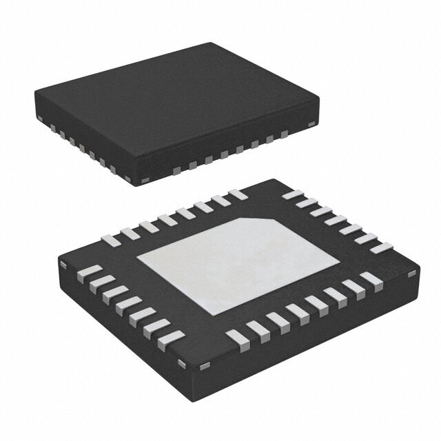
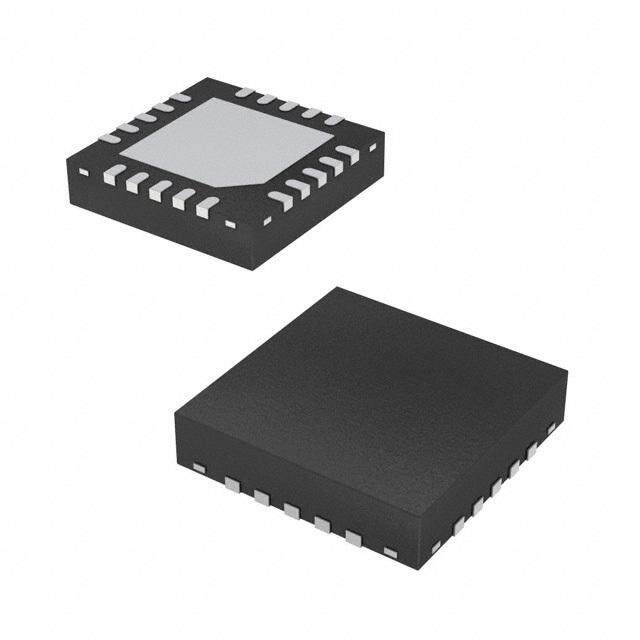
ISL59837IAZ是Renesas Electronics America Inc.推出的一款高性能视频放大器和驱动器,广泛应用于需要高质量模拟视频信号处理的场景。该器件支持多路视频信号放大与缓冲,具备低功耗、高带宽(可达100MHz)和优异的信号完整性,适用于NTSC、PAL、SECAM等标准视频格式。

典型应用场景包括:消费类电子产品如高清电视、机顶盒、DVD播放器中的视频输出驱动;安防监控系统中的摄像机视频信号调理与传输;工业视频设备中对模拟视频信号的缓冲与增强;以及汽车娱乐系统中的后座显示屏视频驱动。其集成的三通道设计可同时处理复合视频(CVBS)、S端子或分量视频(YPbPr)信号,有效简化电路设计。

ISL59837IAZ采用紧凑的16引脚QSOP封装,工作温度范围为-40°C至+85°C,适合工业级环境应用。其低输出失真和快速建立时间确保了清晰、稳定的图像质量,是模拟视频链路中理想的驱动解决方案。
| 参数 | 数值 |
| -3db带宽 | 200MHz |
| 产品目录 | 集成电路 (IC) |
| 描述 | IC VIDEO DRIVER TRUE SGL 16-QSOP |
| 产品分类 | |
| 品牌 | Intersil |
| 数据手册 | |
| 产品图片 |
|
| 产品型号 | ISL59837IAZ |
| rohs | 无铅 / 符合限制有害物质指令(RoHS)规范要求 |
| 产品系列 | - |
| 产品目录页面 | |
| 供应商器件封装 | 16-QSOP |
| 包装 | 管件 |
| 压摆率 | 500 V/µs |
| 安装类型 | 表面贴装 |
| 封装/外壳 | 16-SSOP(0.154",3.90mm 宽) |
| 应用 | 电压反馈 |
| 标准包装 | 97 |
| 电压-电源,单/双 (±) | 3 V ~ 3.6 V |
| 电流-电源 | 97mA |
| 电流-输出/通道 | 80mA |
| 电路数 | 3 |
| 输出类型 | 满摆幅 |


- 商务部:美国ITC正式对集成电路等产品启动337调查
- 曝三星4nm工艺存在良率问题 高通将骁龙8 Gen1或转产台积电
- 太阳诱电将投资9.5亿元在常州建新厂生产MLCC 预计2023年完工
- 英特尔发布欧洲新工厂建设计划 深化IDM 2.0 战略
- 台积电先进制程称霸业界 有大客户加持明年业绩稳了
- 达到5530亿美元!SIA预计今年全球半导体销售额将创下新高
- 英特尔拟将自动驾驶子公司Mobileye上市 估值或超500亿美元
- 三星加码芯片和SET,合并消费电子和移动部门,撤换高东真等 CEO
- 三星电子宣布重大人事变动 还合并消费电子和移动部门
- 海关总署:前11个月进口集成电路产品价值2.52万亿元 增长14.8%


PDF Datasheet 数据手册内容提取
DATASHEET ISL59837 FN6335 200MHz Single Supply Video Driver With Charge Pump and Power Down Rev 1.00 March 5, 2007 The ISL59837 is a revolutionary device that allows true single- Features supply operation of video amplifiers. Designed for systems • Triple single-supply buffer requiring output swing below ground but lacking a negative power supply, the ISL59837 generates the required negative • Generates negative rail from from single +3.3V supply rail internally from a +3.3V power supply. This allows for • No output DC blocking capacitor needed DC-accurate coupling of video onto a 75 double-terminated line. The buffers have an integrated 6dB, eliminating the need • 200MHz -3dB bandwidth for external gain-setting resistors. An external reference • 50MHz 0.1dB bandwidth voltage can be applied to the REF pin to shift the analog video level down by the desired amount. The charge pump and • Fixed gain of 2 output buffer amplifiers can be placed in a power down mode, consuming • Charge pump power down function (0.1mA typical) less than 1mA of current. • Outputs are high impedance in power-down mode Ordering Information • Amplifier enable/disable function control PART NUMBER PART TAPE & PACKAGE PKG. • Pb-free plus anneal available (RoHS compliant) (Note) MARKING REEL (Pb-free) DWG. # Applications ISL59837IAZ 59837 IAZ - 16 Ld QSOP MDP0040 ISL59837IAZ-T7 59837 IAZ 7” 16 Ld QSOP MDP0040 • Driving video NOTE: Intersil Pb-free plus anneal products employ special Pb-free Pinout material sets; molding compounds/die attach materials and 100% matte tin plate termination finish, which are RoHS compliant and ISL59837 compatible with both SnPb and Pb-free soldering operations. Intersil (16 LD QSOP) Pb-free products are MSL classified at Pb-free peak reflow TOP VIEW temperatures that meet or exceed the Pb-free requirements of IPC/JEDEC J STD-020. RIN 1 16ROUT GIN 2 15GOUT BIN 3 14BOUT REF 4 13VCC VEE 5 12EN GND 6 11 VCC VEEOUT 7 10PD DGND 8 9 DVCC FN6335 Rev 1.00 Page 1 of 14 March 5, 2007
ISL59837 Absolute Maximum Ratings Thermal Information VCC, Supply Voltage between VS and GND . . . . . . . . . . . . . . . . .5V Operating Temperature . . . . . . . . . . . . . . . . . . . . . . .-40°C to +85°C VIN, VREF . . . . . . . . . . . . . . . . . . . . . . . . . .VCC+0.3V, VEE-0.3V Maximum Die Temperature . . . . . . . . . . . . . . . . . . . . . . . . . .+150°C Voltage between VIN and VREF. . . . . . . . . . . . . . . . . . . . . . . . . .±2V Storage Temperature. . . . . . . . . . . . . . . . . . . . . . . .-65°C to +150°C Maximum Continuous Output Current. . . . . . . . . . . . . . . . . . . 30mA Lead Temperature . . . . . . . . . . . . . . . . . . . . . . . . . . . . . . . . .+260°C ESD Classification Power Dissipation . . . . . . . . . . . . . . . . . . . . . . . . . . . . . See Curves Human Body Model. . . . . . . . . . . . . . . . . . . . . . . . . . . . . . . . 2000V Pb-free reflow profile . . . . . . . . . . . . . . . . . . . . . . . . . .see link below Machine Model. . . . . . . . . . . . . . . . . . . . . . . . . . . . . . . . . . . . . 200V http://www.intersil.com/pbfree/Pb-FreeReflow.asp CAUTION: Stresses above those listed in “Absolute Maximum Ratings” may cause permanent damage to the device. This is a stress only rating and operation of the device at these or any other conditions above those indicated in the operational sections of this specification is not implied. IMPORTANT NOTE: All parameters having Min/Max specifications are guaranteed. Typical values are for information purposes only. Unless otherwise noted, all tests are at the specified temperature and are pulsed tests, therefore: TJ = TC = TA AC Electrical Specifications VCC = DVCC = +3.3V, REF = GND, TA = +25°C, RL = 150, unless otherwise specified. PARAMETER DESCRIPTION CONDITIONS MIN TYP MAX UNIT BW-3dB 3dB Bandwidth VOUT = 200mVPP 200 MHz VOUT = 2VPP 100 MHz BW 0.1dB 0.1dB Bandwidth VOUT = 2VPP 50 MHz SR Slew Rate VIN = 2VPP 500 V/µs dG Differential Gain 0.07 % dP Differential Phase 0.06 ° XT Hostile Crosstalk 6MHz -90 dB I Input to Output Isolation 6MHz -70 dB VN Input Noise Voltage 20 nV/Hz fCP Charge Pump Switching Frequency 168 MHz Load Reg VEE Load Regulation IEE = 0mA to 10mA 9 30 mV VRIPPLE Output Amp Ripple Voltage 30 mV With Bead Core to DVCC 10 mV DC Electrical Specifications VCC = DVCC = +3.3V, REF = GND, TA = +25°C, RL = 150, unless otherwise specified. PARAMETER DESCRIPTION CONDITIONS MIN TYP MAX UNIT V+ Supply Range 3.0 3.6 V VG% Gain Error RL = 150, VOUT = -1V to +2.5V 1.5 % G Gain Matching RL = 150 0.5 % IIN Analog Input Leakage Current VIN = 0V to 1.5V ±0.1 ±1 µA VOS Output Offset Voltage VREF = 0 -25 7 +25 mV VOUT+ Maximum Output Voltage RL = 75 2.4 2.5 V RL = 150 2.7 2.9 V VOUT- Minimum Output Voltage RL = 75 -1 V RL = 150 -1.2 V IOUT + Output Current RL = 10, VIN = 1.2V 50 80 mA IOUT - Output Current RL = 10, VIN = -0.3V -40 -18 mA ZOUT Disabled Output Impedance EN = 3.3V and/or PD = 3.3V 500 k (Amp Disabled) IREF Reference Input Leakage Current 1 2.3 3.5 µA PSRR Power Supply Rejection Ratio 50 62 dB FN6335 Rev 1.00 Page 2 of 14 March 5, 2007
ISL59837 DC Electrical Specifications VCC = DVCC = +3.3V, REF = GND, TA = +25°C, RL = 150, unless otherwise specified. (Continued) PARAMETER DESCRIPTION CONDITIONS MIN TYP MAX UNIT IS Supply Current EN = PD = GND (Amp Enabled) 97 130 mA EN = 3.3V (Amp Disabled) 60 90 mA IS_PD Power Down Supply Current EN = PD = 3.3V 0.1 1 mA Pin Descriptions PIN NUMBER PIN NAME PIN FUNCTION EQUIVALENT CIRCUIT 1 RIN Analog input VCC VEE CIRCUIT 1 2 GIN Analog input Reference Circuit 1 3 BIN Analog input Reference Circuit 1 4 REF Reference input Hofifgshe ti mofp aemdapnlicfiee risnput controlling VCC GRBIIINNN +- RGBOOOUUUTTT 3 REF x1 VEE CIRCUIT 2 5 VEE Chip substrate (negative power supply VCC for amplifiers) VEE OUT - + DVCC VEE CCHHAARRGGEE PPUUMMPP DGND CIRCUIT 3 6 GND Analog ground 7 VEE OUT Charge pump output Reference Circuit 3 8 DGND Charge pump ground Reference Circuit 3 9 DVCC Charge pump supply voltage Reference Circuit 3 10 PD Power-down Input VCC Low: Normal Operation High: Power-down Charge Pump and Amplifiers VEE CIRCUIT 4 FN6335 Rev 1.00 Page 3 of 14 March 5, 2007
ISL59837 Pin Descriptions (Continued) PIN NUMBER PIN NAME PIN FUNCTION EQUIVALENT CIRCUIT 11, 13 VCC Positive power supply 12 EN Chip Enable Reference Circuit 4 Low: Normal Operation High: Power Down Amplifiers 14 BOUT Analog output VCC VEE CIRCUIT 5 15 GOUT Analog output Reference Circuit 5 16 ROUT Analog output Reference Circuit 5 Typical Performance Curves 3 5 AV = +2 AV = +2 9pF CL = 0pF RL = 500 B) 2 B) 3 4.7pF d d N ( 1 N ( 2.2pF GAI 1k GAI 1 ED 0 ED Z Z LI LI -1 0pF A 500 A M -1 M R R O O N N -3 -2 150 75 -3 -5 1M 10M 100M 1G 100k 1M 10M 100M 1G FREQUENCY (Hz) FREQUENCY (Hz) FIGURE 1. GAIN vs FREQUENCY FOR VARIOUS RLOAD FIGURE 2. GAIN vs FREQUENCY FOR VARIOUS CLOAD 5 300 AV = +2 AV = +2 T (dB) -05 CRLL == 50p00F Hz) 240 RL = 500 -3dB ROLL-OFF U M TP -10 F ( 180 U F O O D -15 L- ALIZE -20 N ROL 120 ORM -25 GAI 60 N -30 -0.1dB ROLL-OFF -35 0 1M 100M 200M 300M 400M 500M 2.25 2.80 3.35 3.90 4.45 5.00 FREQUENCY (Hz) SUPPLY VOLTAGE (V) FIGURE 3. VREF PIN OUTPUT FREQUENCY RESPONSE FIGURE 4. GAIN ROLL-OFF vs FREQUENCY FN6335 Rev 1.00 Page 4 of 14 March 5, 2007
ISL59837 Typical Performance Curves (Continued) -30 -20 AV = +2 AV = +2 -40 RL = 500 -30 RL = 500 -50 -40 dB) -60 B) LK ( -70 ENABLED N (d -50 S TA -80 ATIO -60 ENABLED ROS -90 DISABLED SOL -70 C I -80 DISABLED -100 -110 -90 -120 -100 100k 1M 10M 100M 1G 100k 1M 10M 100M 1G FREQUENCY (Hz) FREQUENCY (Hz) FIGURE 5. CROSS TALK CHANNEL TO CHANNEL (TYPICAL) FIGURE 6. INPUT TO OUTPUT ISOLATION vs FREQUENCY 120 200 AV = +2 RL = 500 -3dB 100 A) 160 RRENT (m 8600 DTH (MHz) 120 ARVL == +5020 CU WI Y D 80 L 40 N P A P B U S 20 40 -0.1dB 0 0 1.0 1.5 2.0 2.5 3.0 3.5 27 47.5 68 88.5 109 129.5 150 SUPPLY VOLTAGE (V) TEMPERATURE (°C) FIGURE 7. SUPPLY CURRENT vs SUPPLY VOLTAGE FIGURE 8. BANDWIDTH vs TEMPERATURE 95 100 AV = +2 RL = 500 A) m 90 10 T ( ) EN E ( R C UR 85 AN 1 C D PLY MPE UP 80 I 0.1 S 75 0.01 27 55.6 84.2 112.8 141.4 170 10k 100k 1M 10M 100M TEMPERATURE (°C) FREQUENCY (Hz) FIGURE 9. SUPPLY CURRENT vs TEMPERATURE FIGURE 10. OUTPUT IMPEDANCE vs FREQUENCY FN6335 Rev 1.00 Page 5 of 14 March 5, 2007
ISL59837 Typical Performance Curves (Continued) 0 1k VCC = DVCC = 3.3V -10 VAC = 100mVP-P -20 RL = 150 V/Hz),A/Hz) 100 R (dB) --4300 OISE (nOISE (p 10 eN R NN PS -50 GE NT -60 LTARRE 1 IN+ OU VC IN- -70 -80 0.1 10k 100k 1M 10M 10 100 1k 10k 100k 1M 10M FREQUENCY (Hz) FREQUENCY (Hz) FIGURE 11. POWER SUPPLY REJECTION RATIO vs FIGURE 12. VOLTAGE AND CURRENT NOISE vs FREQUENCY FREQUENCY -30 -30 Bc) -40 -40 d N ( -50 THD ORTIO -60 Bc) -50 THD DIST -70 2ND HD HD (d -60 FIN = 10MHz C T ONI -80 3RD HD -70 M AR -90 -80 THD H FIN = 1MHz -100 -90 0M 10M 20M 30M 40M 0.5 1.0 1.5 2.0 2.5 3.0 3.5 FUNDAMENTAL FREQUENCY (Hz) OUTPUT VOLTAGE (VP-P) FIGURE 13. HARMONIC DISTORTION vs FREQUENCY FIGURE 14. THD vs OUTPUT VOLTAGE 0 0 L -0.02 L FFERENTIAGAIN (%) -0.04 FFERENTIAPHASE (°) --00..0042 DI DI -0.06 -0.06 -0.08 -0.08 IRE IRE FIGURE 15. DIFFERENTIAL GAIN FIGURE 16. DIFFERENTIAL PHASE FN6335 Rev 1.00 Page 6 of 14 March 5, 2007
ISL59837 Typical Performance Curves (Continued) V) V) DI DI V/ V/ m m 0 0 0 0 5 5 S ( S ( T T L L O O V V TIME (200ns/DIV) TIME (200ns/DIV) FIGURE 17. DISABLE TIME FIGURE 18. ENABLE TIME DIV) DIV) mV/ mV/ OLTS (50 OLTS (500 V V TIME (10ns/DIV) TIME (10ns/DIV) FIGURE 19. SMALL SIGNAL RISE AND FALL TIME FIGURE 20. LARGE SIGNAL RISE AND FALL TIMES 0 3.25 -10 -20 V) V) -30 GE ( 3.00 B -40 N SE (d -50 T RA OI U N -60 TP 2.75 U -70 O -80 AV = +2 CL = 3.9pF -90 2.50 0 100 200 300 400 500 600 700 800 900 1000 50 250 450 650 850 1050 FREQUENCY (Hz) LOAD RESISTANCE () FIGURE 21. NOISE FLOOR WITH CHARGE PUMP HARMONICS FIGURE 22. MAXIMUM OUTPUT MAGNITUDE vs LOAD RESISTANCE FN6335 Rev 1.00 Page 7 of 14 March 5, 2007
ISL59837 Typical Performance Curves (Continued) 1.6 1.6 BACKDRIVE ACROSS 5 RESISTOR AV = +2 A) TYPICAL CHANNEL RL = 500 m CL = 3.9pF T ( 1.2 1.2 N E B) R d CUR 0.8 NG ( 0.8 E KI V A RI E D P CK 0.4 0.4 A B 0 0 0 1 2 3 4 5 2.2 2.4 2.6 2.8 3.0 3.2 3.4 3.6 3.8 4.0 BACKDRIVE VOLTAGE (V) SUPPLY VOLTAGE (V) FIGURE 23. BACKDRIVE VOLTAGE vs CURRENT FIGURE 24. PEAKING vs SUPPLY VOLTAGE JEDEC JESD51-3 LOW EFFECTIVE THERMAL JEDEC JESD51-7 HIGH EFFECTIVE THERMAL CONDUCTIVITY TEST BOARD CONDUCTIVITY TEST BOARD 1.4 1.8 1.6 1.2 W) W) 1.4 ON ( 1.0 ON ( 1.2 1.116W TI 791mW TI ER DISSIPA 000...864 JA =Q +S1O58P°1C6/W ER DISSIPA 100...086 JA = +Q1S1O2P°C1/6W W W O O 0.4 P 0.2 P 0.2 0 0 0 25 50 75 85 100 125 150 0 25 50 75 85 100 125 150 AMBIENT TEMPERATURE (°C) AMBIENT TEMPERATURE (°C) FIGURE 25. PACKAGE POWER DISSIPATION vs AMBIENT FIGURE 26. PACKAGE POWER DISSIPATION vs AMBIENT TEMPERATURE TEMPERATURE FN6335 Rev 1.00 Page 8 of 14 March 5, 2007
ISL59837 Block Diagram VCC RIN + 6dB ROUT - REF GIN + 6dB GOUT - BIN + 6dB BOUT - DVCC CHARGE PUMP VEE-OUT VEE VOUT = 2VIN - VREFERENCE Demo Board Schematic RED_IN R1 75 RED_OUT R4 75 GREEN_IN 1 RIN ROUT16 R2 R5 75 75 2 GIN GOUT15 GREEN_OUT R6 75 3 BIN BOUT14 VCC BLUE_IN 4 REF VCC13 BLUE_OUT R3 C4 C3 75 0.1µF 5 VEE EN12 0.1µF 6 GND VCC 11 VCC 2 1 7 VEEOUT PD10 DISABLE C2 R4 R8 0.1µF C5 0.1µF 3 VCC 8 DGND DVCC 9 ENABLE 499 1k OFFSET Option: Panasonic 120Bead CONTROL EXC3BP121H Lower Amp output noise from charge pump FN6335 Rev 1.00 Page 9 of 14 March 5, 2007
MaFN ISL59837 + DC-Restore Solution ISL rch 56335 5983 , 2R 7 0e 0v 7 1 11 IINN11 IINN221166 .0 0 22 CCOOMM11 CCOOMM221155 33 NC1 NC21144 44 VV-- VV++1133 RR77 22kk 55 GND NC1122 (No Connect) 66 NC4 NC31111 77 CCOOMM44 CCOOMM331100 YYOO RR11 88 IINN44 IINN33 99 CN = Option for lower 7755 IISSLL4433114400 RR99 R10 charge pump noise 22kk 22kk YYOO C12 PPbb CC44 00..11µµFF 11 RRIINN RROOUUTT1166 RR44 7755 2200ppFF RR22 C5 00..11µµFF RR55 7755 7755 22 GGIINN GGOOUUTT1155 PPbb C13 C6 00..11µµFF 33 BBIINN BBOOUUTT1144 RR66 7755 2200ppFF VVCCCC PPrr 44 RREEFF VVCCCC1133 PPrr RR33 C7 VVEEEE ((--11..66VV)) C1 C14 7755 0.1µF 55 VVEEEE EENN1122 00..11µµFF 2200ppFF 66 GGNNDD VVCCCC 1111 EENNAABBLLEE VCC 22 11 VVCCCC VVCCCC OFFSET C11 77 VVEEEEOOUUTT NNCC1100 VVCCCC ++C16 CONTROL 00..11µµFF 00..11µµFF 33 11µµFF 88 DDGGNNDD DDVVCCCC 99 GGNNDD C15 IISSLL5599883300 11 CCOOMMPP VVDDDD 88 Option: Panasonic 120Bead CC44 SSYYNNCC OOUUTT C8 EXC3BP121H 22 CCOOMMPP OOUUTT 77 00..11µµFF Lower Amp output noise from charge pump VVIIDDEEOO IINN 00..11µµFF 33 VVSSYYNNCC RREESSEETT 66 OOUUTT BBAACCKK C9 R13 Pag C10 44 GGNNDD PPOORROOCCUUHHTT 55 0.1µF 681k e 0.1µF EELL11888811 1 0 o f 1 4
ISL59837 Description of Operation and Application distortion, low power, and high frequency amplifier capable of Information driving moderately capacitive loads with near rail-to-rail performance. Theory Of Operation INPUT OUTPUT RANGE The ISL59837 is a highly practical and robust marriage of three The three amplifier channels have an input common mode high bandwidth, high speed, low power, rail-to-rail voltage voltage range from 0.15V below the bottom rail to within feedback amplifiers with a charge pump to provide a negative rail without an additional power supply. Designed to operate 100mV of the positive supply, VS+ pin (Note: bottom rail is established by the charge pump at negative one half the with a single supply voltage range from 0V to 3.3V, the positive supply). As the input signal moves outside the ISL59837 eliminates the need for a split supply with the specified range, the output signal will exhibit increasingly incorporation of a charge pump capable of generating a bottom higher levels of harmonic distortion. And of course, as load rail as much as 1.6V below ground for a 4.9V range on a single resistance becomes lower, the current drive capability of the 3.3V supply. This performance is ideal for NTSC video with its device will be challenged and its ability to drive close to each negative-going sync pulses. rail is reduced. For instance, with a load resistance of 1k the THE AMPLIFIER output swing is within 100mV of the rails, while a load The ISL59837 fabricated on a di-electrically isolated high resistance of 150 limits the output swing to within around speed 5V Bi-CMOS process with 4GHz PNPs and NPN 300mV of the rails. transistor exceeding 20GHz - perfect for low distortion, low AMPLIFIER OUTPUT IMPEDANCE power demand and high frequency circuits. While the To achieve near rail-to-rail performance, the output stage of the ISL59837 utilizes somewhat standard voltage mode feedback ISL59837 uses transistors in the common emitter topologies, there are many non-standard analog features configuration, typically producing higher output impedance providing its outstanding bandwidth, rail-to-rail operation, and than the standard emitter follower output stage. The output drive capabilities. The input signal initially passes exceptionally high open loop gain of the ISL59837 and local through a folded cascode, a topology providing enhanced feedback reduces output impedance to less than 2 at low frequency response by essentially fixing the base collector frequency. However, since output impedance of the device is voltage at the junction of the input and gain stage. The exponentially modulated by the magnitude of the open loop collector of each input device looks directly into an emitter that gain, output impedance increases with frequency as the open is tied closely to ground through a resistor and biased with a loop gain decreases with frequency. This inductive-like effect of very stable DC source. Since the voltage of this collector is the output impedance is countered in the ISL59837 with "locked stable," the effective bandwidth limiting of the Miller proprietary output stage topology, keeping the output capacitance is greatly reduced. The signal is then passed impedance low over a wide frequency range and making it through a second fully-realized differential gain stage and possible to easily and effectively drive relatively heavy finally through a proprietary common emitter output stage for capacitive loads (see Figure 10). improved rail-to-rail output performance. The result is a highly-stable, low IN+ IN- OUT BIAS FIGURE 27. SIMPLIFIED SCHEMATIC FN6335 Rev 1.00 Page 11 of 14 March 5, 2007
ISL59837 THE CHARGE PUMP has been eliminated with the incorporation of a charge pump capable of generating a bottom rail as much as 1.6V below The ISL59837 charge pump provides a bottom rail up to 1.6V ground, for a 4.9V range on a single 3.3V supply. This below ground while operating on a 0V to 3.3V power supply. performance is ideal for NTSC video with its negative-going The charge pump is internally regulated to one-half the sync pulses. potential of the positive supply. This internal multi-phase charge pump is driven by a 110MHz differential ring oscillator VIDEO PERFORMANCE driving a series of inverters and charge storage circuitry. Each For good video performance, an amplifier is required to maintain series inverter charges and places parallel adjoining charge the same output impedance and the same frequency and phase circuitry slightly out of phase with the immediately preceding response as DC levels are changed at the output. This is block. This generates a negative rail of about -1.6V with a low especially difficult when driving a standard video load of 150 amplitude ripple voltage from the charge pump action. Some of because of the change in output current with changing DC this ripple is coupled into the output signals at a very low levels. Special circuitry has been incorporated into the ISL59837 amplitude, as seen in Figure 21. The ripple on the outputs is for the reduction of output impedance variation with the current typically well below the noise floor of the signal. output. This results in outstanding differential gain and There are two ways to further reduce the output supply noise: differential phase specifications of 0.06% and 0.1°, while driving 150 at a gain of +2. Driving higher impedance loads would • Add a 120bead in series between VCC and DVCC. This result in similar or better differential gain and differential phase reduces the coupling between the charge pump and the performance. analog amplifier supplies. NTSC • Add a 20pF capacitor between the back load 75 resistor and ground (see “ISL59837 + DC-Restore Solution” on The ISL59837 (generating a negative rail internally) is ideally page10). This will attenuate frequencies above 100MHz. suited for NTSC video with its accompanying negative-going sync signals, which is easily handled by the ISL59837 without The system operates at sufficiently high frequencies that any the need for an additional supply as the ISL59837 generates a related charge pump noise is far beyond standard video negative rail with an internal charge pump referenced at bandwidth requirements. Still, appropriate bypassing discipline negative 1/2 the positive supply. must be observed, and all pins related to either the power supply or the charge pump must be properly bypassed. See YPbPr “Power Supply Bypassing and Printed Circuit Board Layout” on YPbPr signals originating from a DVD player requiring three page13. channels of very tightly-controlled amplifier gain accuracy present THE VREF PIN no difficulty for the ISL59837. Specifically, this standard encodes sync on the Y-Channel and it is a negative-going signal, which is Applying a voltage to the VREF pin simply places that voltage easily handled by the ISL59837 without the need for an additional on what would usually be the ground side of the gain resistor of supply as the ISL59837 generates a negative rail placed at the amplifier, resulting in a DC-level shift of the output signal. negative 1/2 the positive supply. Additionally, the Pb and Pr are Applying 100mV to the VREF pin would apply a 100mV DC bipolar analog signals and the video signals are negative-going, level shift to the outgoing signal. The charge pump provides and again, easily handled by the ISL59837. sufficient bottom room to accommodate the shifted signal. DRIVING CAPACITIVE LOADS AND CABLES The ISL59837 buffers the VREF voltage before applying it to the triple amplifiers, isolating the input from the amplifiers and The ISL59837 (internally-compensated to drive 75 cables) will allowing it to be driven by moderate-impedance voltage drive 10pF loads in parallel with 1k with less than 5dB of sources. peaking. If less peaking is required, a small series resistor, usually between 5 to 50, can be placed in series with the output. This THE VEE PIN will reduce peaking at the expense of a slight closed loop gain The VEE pin is the output pin for the charge pump. A voltmeter reduction. When used as a cable driver, double termination is applied to this pin will display the output of the charge pump. always recommended for reflection-free performance. For those This pin does not affect the functionality of the part. One may applications, a back-termination series resistor at the amplifier's use this pin as an additional voltage source. Keep in mind that output will isolate the amplifier from the cable and allow extensive the output of this pin is generated by the internal charge pump capacitive drive. However, other applications may have high and a fully regulated supply that must be properly bypassed. capacitive loads without a back-termination resistor. Again, a We recommend a 0.1µF ceramic capacitor placed as close to small series resistor at the output can help to reduce peaking. The the pin and connected to the ground plane of the board. ISL59837 is a triple amplifier designed to drive three channels; simply deal with each channel separately as described in this INPUT, OUTPUT AND SUPPLY VOLTAGE RANGE section. The ISL59837 is designed to operate with a single supply voltage range of from 0V to 3.3V. The need for a split supply FN6335 Rev 1.00 Page 12 of 14 March 5, 2007
ISL59837 DC-RESTORE for sinking: When the ISL59837 is AC-coupled it becomes necessary to PD = V I +V i–V I i restore the DC reference for the signal. This is accomplished MAX S SMAX OUT S LOAD (EQ. 3) with a DC-restore system applied between the capacitive "AC" coupling and the input of the device. Refer to “ISL59837 + DC- Where: Restore Solution” on page10. VS = Supply voltage DISABLE/POWER-DOWN ISMAX = Maximum quiescent supply current The ISL59837 can be disabled and its output placed in a high impedance state. The turn-off time is around 25ns and the turn- VOUT = Maximum output voltage of the application on time is around 200ns. When the PD pin is taken high, the RLOAD = Load resistance tied to ground chip’s total supply current is reduced to 0.1mA typically, all but eliminating the power used by the part. Taking the EN pin high ILOAD = Load current powers down the amplifiers, leaving the charge pump running. i = Number of output channels Both pins can be controlled by standard TTL or CMOS signal levels (0.8V VIL, 2.0V VIH relative to GND). By setting the two PDMAX equations equal to each other, we can solve the output current and RLOAD to avoid the device OUTPUT DRIVE CAPABILITY overheat. The ISL59837 does not have internal short-circuit protection Power Supply Bypassing and Printed Circuit Board circuitry. A short-circuit current of 80mA sourcing and 150mA Layout sinking for the output is connected half way between the rails with a 10 resistor. If the output is shorted indefinitely, the power Strip line design techniques are recommended for the input dissipation could easily increase such that the part will be and output signal traces. As with any high frequency device, a destroyed. Maximum reliability is maintained if the output current good printed circuit board layout is necessary for optimum never exceeds ±40mA, after which the electro-migration limit of performance. Lead lengths should be as short as possible. The the process will be exceeded and the part will be damaged. This power supply pin must be well bypassed to reduce the risk of limit is set by the design of the internal metal interconnections. oscillation. For normal single supply operation, where the VS- pin is connected to the ground plane, a single 4.7µF tantalum POWER DISSIPATION capacitor in parallel with a 0.1µF ceramic capacitor from VS+ to With the high output drive capability of the ISL59837, it is GND will suffice. This same capacitor combination should be possible to exceed the +150°C absolute maximum junction placed at each supply pin to ground if split-internal supplies are temperature under certain load current conditions. Therefore, it to be used. In this case, the VS- pin becomes the negative is important to calculate the maximum junction temperature for supply rail. an application to determine if load conditions or package types For good AC performance, parasitic capacitance should be need to be modified to assure operation of the amplifier in a kept to a minimum. Use of wire-wound resistors should be safe operating area. avoided because of their additional series inductance. Use of The maximum power dissipation allowed in a package is sockets should also be avoided if possible. Sockets add determined according to Equation 1: parasitic inductance and capacitance can result in T –T compromised performance. Minimizing parasitic capacitance PDMAX = ----J---M-----A----X--------------A---M-----A----X--- (EQ. 1) at the amplifier's inverting input pin is also very important. JA Where: TJMAX = Maximum junction temperature TAMAX = Maximum ambient temperature JA = Thermal resistance of the package The maximum power dissipation actually produced by an IC is the total quiescent supply current times the total power supply voltage, plus the power in the IC due to the load, or: for sourcing: V i OUT PD = V I +V –V i----------------- MAX S SMAX S OUT R i L (EQ. 2) FN6335 Rev 1.00 Page 13 of 14 March 5, 2007
ISL59837 Quarter Size Outline Plastic Packages Family (QSOP) A MDP0040 D QUARTER SIZE OUTLINE PLASTIC PACKAGES FAMILY N (N/2)+1 INCHES SYMBOL QSOP16 QSOP24 QSOP28 TOLERANCE NOTES A 0.068 0.068 0.068 Max. - PIN #1 I.D. MARK E E1 A1 0.006 0.006 0.006 ±0.002 - A2 0.056 0.056 0.056 ±0.004 - b 0.010 0.010 0.010 ±0.002 - 1 (N/2) c 0.008 0.008 0.008 ±0.001 - B D 0.193 0.341 0.390 ±0.004 1, 3 0.010 CAB E 0.236 0.236 0.236 ±0.008 - e E1 0.154 0.154 0.154 ±0.004 2, 3 H e 0.025 0.025 0.025 Basic - C SEATING L 0.025 0.025 0.025 ±0.009 - PLANE L1 0.041 0.041 0.041 Basic - 0.004 C 0.007 CAB b N 16 24 28 Reference - Rev. F 2/07 L1 NOTES: 1. Plastic or metal protrusions of 0.006” maximum per side are not A included. 2. Plastic interlead protrusions of 0.010” maximum per side are not c included. SEE DETAIL "X" 3. Dimensions “D” and “E1” are measured at Datum Plane “H”. 4. Dimensioning and tolerancing per ASME Y14.5M-1994. 0.010 A2 GAUGE PLANE L A1 4°±4° DETAIL X © Copyright Intersil Americas LLC 2006-2007. All Rights Reserved. All trademarks and registered trademarks are the property of their respective owners. For additional products, see www.intersil.com/en/products.html Intersil products are manufactured, assembled and tested utilizing ISO9001 quality systems as noted in the quality certifications found at www.intersil.com/en/support/qualandreliability.html Intersil products are sold by description only. Intersil may modify the circuit design and/or specifications of products at any time without notice, provided that such modification does not, in Intersil's sole judgment, affect the form, fit or function of the product. Accordingly, the reader is cautioned to verify that datasheets are current before placing orders. Information furnished by Intersil is believed to be accurate and reliable. However, no responsibility is assumed by Intersil or its subsidiaries for its use; nor for any infringements of patents or other rights of third parties which may result from its use. No license is granted by implication or otherwise under any patent or patent rights of Intersil or its subsidiaries. For information regarding Intersil Corporation and its products, see www.intersil.com FN6335 Rev 1.00 Page 14 of 14 March 5, 2007