ICGOO在线商城 > 集成电路(IC) > 线性 - 放大器 - 视频放大器和频缓冲器 > CGD1046HI,112

 Datasheet下载
- 型号: CGD1046HI,112
- 制造商: NXP Semiconductors
- 库位|库存: xxxx|xxxx
- 要求:
| 数量阶梯 | 香港交货 | 国内含税 |
| +xxxx | $xxxx | ¥xxxx |
查看当月历史价格
查看今年历史价格
CGD1046HI,112产品简介:
ICGOO电子元器件商城为您提供CGD1046HI,112由NXP Semiconductors设计生产,在icgoo商城现货销售,并且可以通过原厂、代理商等渠道进行代购。 CGD1046HI,112价格参考¥183.49-¥356.36。NXP SemiconductorsCGD1046HI,112封装/规格:线性 - 放大器 - 视频放大器和频缓冲器, Video Amp, 1 CATV SOT115J。您可以下载CGD1046HI,112参考资料、Datasheet数据手册功能说明书,资料中有CGD1046HI,112 详细功能的应用电路图电压和使用方法及教程。
型号为CGD1046HI,112的芯片由NXP USA Inc.生产,属于线性放大器中的视频放大器和频率缓冲器类别。该器件主要应用于需要高频信号处理和放大的场景。

CGD1046HI,112是一款高频率、高增益的射频(RF)放大器,常用于无线通信系统中的信号增强,如蜂窝基站、无线接入网络(WAN)设备、微波通信系统和广播设备。作为频率缓冲器,它还可用于隔离前后级电路,防止信号干扰和失真,提高系统稳定性。

此外,该器件适用于测试设备和测量仪器中的信号调理模块,确保高频信号的准确传输和放大。由于其良好的高频性能和可靠性,也常见于航空航天和国防领域的雷达系统和电子战设备中。

总的来说,CGD1046HI,112适用于需要高频率、高稳定性和高性能信号放大的通信和电子系统中,发挥着信号增强与隔离缓冲的重要作用。
| 参数 | 数值 |
| -3db带宽 | - |
| 产品目录 | 集成电路 (IC)半导体 |
| 描述 | IC PWR DOUBLER 1GHZ 27DB SOT115射频放大器 1CH 4.5dB 24V 450mA |
| 产品分类 | |
| 品牌 | NXP Semiconductors |
| 产品手册 | |
| 产品图片 |
|
| rohs | 符合RoHS无铅 / 符合限制有害物质指令(RoHS)规范要求 |
| 产品系列 | RF集成电路,射频放大器,NXP Semiconductors CGD1046HI,112- |
| 数据手册 | |
| 产品型号 | CGD1046HI,112 |
| PCN封装 | |
| 产品种类 | 射频放大器 |
| 供应商器件封装 | SOT115J |
| 其它名称 | 568-5231 |
| 功率增益类型 | 27 dB |
| 包装 | 散装 |
| 压摆率 | - |
| 商标 | NXP Semiconductors |
| 噪声系数 | 5 dB |
| 安装类型 | - |
| 安装风格 | SMD/SMT |
| 封装 | Tube |
| 封装/外壳 | SOT-115J |
| 封装/箱体 | SOT-115J |
| 工作电源电压 | 24 V |
| 工作频率 | 40 MHz to 1.003 GHz |
| 工厂包装数量 | 100 |
| 应用 | CATV |
| 最大工作温度 | + 100 C |
| 最小工作温度 | - 20 C |
| 标准包装 | 25 |
| 测试频率 | 1.003 GHz |
| 电压-电源,单/双 (±) | - |
| 电流-电源 | 450mA |
| 电流-输出/通道 | - |
| 电源电流 | 450 mA |
| 电路数 | 1 |
| 类型 | General Purpose Amplifier |
| 输出类型 | - |
| 通道数量 | 1 Channel |


- 商务部:美国ITC正式对集成电路等产品启动337调查
- 曝三星4nm工艺存在良率问题 高通将骁龙8 Gen1或转产台积电
- 太阳诱电将投资9.5亿元在常州建新厂生产MLCC 预计2023年完工
- 英特尔发布欧洲新工厂建设计划 深化IDM 2.0 战略
- 台积电先进制程称霸业界 有大客户加持明年业绩稳了
- 达到5530亿美元!SIA预计今年全球半导体销售额将创下新高
- 英特尔拟将自动驾驶子公司Mobileye上市 估值或超500亿美元
- 三星加码芯片和SET,合并消费电子和移动部门,撤换高东真等 CEO
- 三星电子宣布重大人事变动 还合并消费电子和移动部门
- 海关总署:前11个月进口集成电路产品价值2.52万亿元 增长14.8%


PDF Datasheet 数据手册内容提取
CGD1046HI 1 GHz, 27 dB gain GaAs high output power doubler Rev. 1 — 30 July 2010 Product data sheet 1. Product profile 1.1 General description Hybrid amplifier module in a SOT115J package, operating at a supply voltage of 24V Direct Current (DC), employing Hetero junction Field Effect Transistor (HFET) GaAs dies. 1.2 Features and benefits (cid:132) Excellent linearity (cid:132) Superior levels of ESD protection (cid:132) Extremely low noise (cid:132) Excellent return loss properties (cid:132) Gain compensation over temperature (cid:132) Rugged construction (cid:132) Unconditionally stable (cid:132) Thermally optimized design (cid:132) Compliant to Directive 2002/95/EC, regarding Restriction of the use of certain Hazardous Substances (RoHS) (cid:132) Integrated ring wave surge protection 1.3 Applications (cid:132) CATV systems operating in the 40MHz to1003MHz frequency range 1.4 Quick reference data Table 1. Quick reference data Bandwidth 40 MHz to 1003 MHz; V =24V (DC); Z = Z = 75Ω; T =35°C; unless otherwise B S L mb specified. Symbol Parameter Conditions Min Typ Max Unit G power gain f=45MHz - 25.5 - dB p f=1003MHz 26.5 27 28 dB CTB composite triple beat V = 56.4 dBmV at 1003 MHz [1] - −75 −65 dBc o CCN carrier-to-composite noise V = 56.4 dBmV at 1003 MHz [1] 57 63 - dBc o I total current [2] - 450 465 mA tot [1] 79 NTSC channels [f = 54 MHz to 550 MHz] + 75 digital channels [f = 550 MHz to 1003 MHz] (−6dB offset); tilt extrapolated to 13.5dB at 1003MHz. [2] Direct Current (DC).
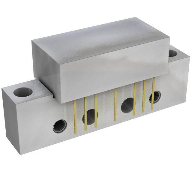
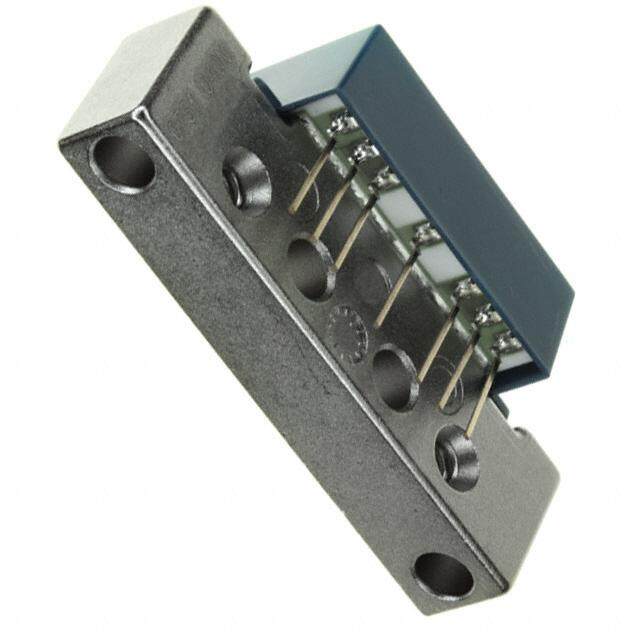
CGD1046HI NXP Semiconductors 1 GHz, 27 dB gain GaAs high output power doubler 2. Pinning information Table 2. Pinning Pin Description Simplified outline Graphic symbol 1 input 2, 3 common 1 3 5 7 9 5 1 9 5 +V B 7, 8 common 2 3 7 8 9 output sym095 3. Ordering information Table 3. Ordering information Type number Package Name Description Version CGD1046HI - rectangular single-ended package; aluminium flange; SOT115J 2vertical mounting holes; 2×6-32UNC and 2extra horizontal mounting holes; 7gold-plated in-line leads 4. Limiting values Table 4. Limiting values In accordance with the Absolute Maximum Rating System (IEC 60134). Symbol Parameter Conditions Min Max Unit V supply voltage - 30 V B V RF input voltage single tone - 75 dBmV i(RF) V electrostatic discharge voltage HumanBodyModel(HBM); [1] - 2000 V ESD According JEDEC standard 22-A114E Biased; According - 1500 V IEC61000-4-2 T storage temperature −40 +100 °C stg T mounting base temperature −20 +100 °C mb [1] The ESD pulse of 2000 V corresponds to a class 2 sensitivity level. CGD1046HI All information provided in this document is subject to legal disclaimers. © NXP B.V. 2010. All rights reserved. Product data sheet Rev. 1 — 30 July 2010 2 of 8
CGD1046HI NXP Semiconductors 1 GHz, 27 dB gain GaAs high output power doubler 5. Characteristics Table 5. Characterist ics Bandwidth 40 MHz to 1003 MHz; V =24V (DC); Z = Z = 75Ω; T =35°C; unless otherwise specified. B S L mb Symbol Parameter Conditions Min Typ Max Unit G power gain f = 45 MHz - 25.5 - dB p f = 1003 MHz 26.5 27 28 dB SL slope straight line f = 45MHzto1003MHz [1] 0.7 - 2.2 dB sl FL flatness of frequency response f = 45MHzto1003MHz [2] - - 1 dB RL input return loss f=45MHzto160MHz 20 - - dB in f=160MHzto320MHz 19 - - dB f=320MHzto640MHz 18 - - dB f=640MHzto870MHz 17 - - dB f=870MHzto1003MHz 16 - - dB RL output return loss f=45MHzto160MHz 20 - - dB out f=160MHzto320MHz 18 - - dB f=320MHzto640MHz 17 - - dB f=640MHzto870MHz 16 - - dB f=870MHzto1003MHz 16 - - dB NF noise figure f=50MHz - 4.5 5.5 dB f=1003MHz - 5 6 dB I total current [3] - 450 465 mA tot 79 NTSC channels + 75 digital channels CTB composite triple beat V = 56.4 dBmV at 1003 MHz [4] - −75 −65 dBc o CSO composite second-order distortion V = 56.4 dBmV at 1003 MHz [4] - −70 −63 dBc o Xmod cross modulation V = 56.4 dBmV at 1003 MHz [4] - −68 - dB o CCN carrier-to-composite noise V = 56.4 dBmV at 1003 MHz [4] 57 63 - dBc o 79 NTSC channels CTB composite triple beat V = 58.4 dBmV at 1003 MHz [5] - −70 - dBc o CSO composite second-order distortion V = 58.4 dBmV at 1003 MHz [5] - −67 - dBc o Xmod cross modulation V = 58.4 dBmV at 1003 MHz [5] - −64 - dB o [1] G at 1003 MHz minus G at 45 MHz. p p [2] Flatness is defined as peak deviation to straight line. [3] Direct Current (DC). [4] 79 NTSC channels [f = 54 MHz to 550 MHz] + 75 digital channels [f = 550 MHz to 1003 MHz] (−6dB offset); tilt extrapolated to 13.5dB at 1003MHz. [5] 79 NTSC channels [f = 54 MHz to 550 MHz]; tilt extrapolated to 13.5dB at 1003MHz. CGD1046HI All information provided in this document is subject to legal disclaimers. © NXP B.V. 2010. All rights reserved. Product data sheet Rev. 1 — 30 July 2010 3 of 8
CGD1046HI NXP Semiconductors 1 GHz, 27 dB gain GaAs high output power doubler 6. Package outline Rectangular single-ended package; aluminium flange; 2 vertical mounting holes; 2 x 6-32 UNC and 2 extra horizontal mounting holes; 7 gold-plated in-line leads SOT115J D E Z p A2 1 2 3 5 7 8 9 A L F S c W e b w M d e1 U2 Q q2 y M B B q1 x M B y M B p U1 q 0 5 10 mm scale DIMENSIONS (mm are the original dimensions) UNITmAax. mAa2x. b c mDax. d mEax. e e1 F mLin. p mQax. q q1 q2 S U1 U2 W w x y mZax. 0.51 2.04 4.15 44.75 8.2 6-32 mm 20.8 9.5 0.25 27.2 13.75 2.54 5.08 12.7 8.8 2.4 38.1 25.4 10.2 4.2 0.25 0.7 0.1 3.8 0.38 2.54 3.85 44.25 7.8 UNC OUTLINE REFERENCES EUROPEAN ISSUE DATE VERSION IEC JEDEC JEITA PROJECTION 04-02-04 SOT115J 10-06-18 Fig 1. Package outline SOT115J CGD1046HI All information provided in this document is subject to legal disclaimers. © NXP B.V. 2010. All rights reserved. Product data sheet Rev. 1 — 30 July 2010 4 of 8
CGD1046HI NXP Semiconductors 1 GHz, 27 dB gain GaAs high output power doubler 7. Abbreviations Table 6. Abbreviations Acronym Description CATV Community Antenna TeleVision ESD ElectroStatic Discharge GaAs Gallium-Arsenide NTSC National Television Standard Committee RF Radio Frequency UNC UNified Coarse 8. Revision history Table 7. Revision history Document ID Release date Data sheet status Change notice Supersedes CGD1046HI v.1 20100730 Product data sheet - - CGD1046HI All information provided in this document is subject to legal disclaimers. © NXP B.V. 2010. All rights reserved. Product data sheet Rev. 1 — 30 July 2010 5 of 8
CGD1046HI NXP Semiconductors 1 GHz, 27 dB gain GaAs high output power doubler 9. Legal information 9.1 Data sheet status Document status[1][2] Product status[3] Definition Objective [short] data sheet Development This document contains data from the objective specification for product development. Preliminary [short] data sheet Qualification This document contains data from the preliminary specification. Product [short] data sheet Production This document contains the product specification. [1] Please consult the most recently issued document before initiating or completing a design. [2] The term ‘short data sheet’ is explained in section “Definitions”. [3] The product status of device(s) described in this document may have changed since this document was published and may differ in case of multiple devices. The latest product status information is available on the Internet at URLhttp://www.nxp.com. 9.2 Definitions malfunction of an NXP Semiconductors product can reasonably be expected to result in personal injury, death or severe property or environmental damage. NXP Semiconductors accepts no liability for inclusion and/or use of Draft — The document is a draft version only. The content is still under NXP Semiconductors products in such equipment or applications and internal review and subject to formal approval, which may result in therefore such inclusion and/or use is at the customer’s own risk. modifications or additions. NXP Semiconductors does not give any representations or warranties as to the accuracy or completeness of Applications — Applications that are described herein for any of these information included herein and shall have no liability for the consequences of products are for illustrative purposes only. NXP Semiconductors makes no use of such information. representation or warranty that such applications will be suitable for the specified use without further testing or modification. Short data sheet — A short data sheet is an extract from a full data sheet with the same product type number(s) and title. A short data sheet is intended Customers are responsible for the design and operation of their applications for quick reference only and should not be relied upon to contain detailed and and products using NXP Semiconductors products, and NXP Semiconductors full information. For detailed and full information see the relevant full data accepts no liability for any assistance with applications or customer product sheet, which is available on request via the local NXP Semiconductors sales design. It is customer’s sole responsibility to determine whether the NXP office. In case of any inconsistency or conflict with the short data sheet, the Semiconductors product is suitable and fit for the customer’s applications and full data sheet shall prevail. products planned, as well as for the planned application and use of customer’s third party customer(s). Customers should provide appropriate Product specification — The information and data provided in a Product design and operating safeguards to minimize the risks associated with their data sheet shall define the specification of the product as agreed between applications and products. NXP Semiconductors and its customer, unless NXP Semiconductors and NXP Semiconductors does not accept any liability related to any default, customer have explicitly agreed otherwise in writing. In no event however, damage, costs or problem which is based on any weakness or default in the shall an agreement be valid in which the NXP Semiconductors product is customer’s applications or products, or the application or use by customer’s deemed to offer functions and qualities beyond those described in the third party customer(s). Customer is responsible for doing all necessary Product data sheet. testing for the customer’s applications and products using NXP Semiconductors products in order to avoid a default of the applications and 9.3 Disclaimers the products or of the application or use by customer’s third party customer(s). NXP does not accept any liability in this respect. Limited warranty and liability — Information in this document is believed to Limiting values — Stress above one or more limiting values (as defined in be accurate and reliable. However, NXP Semiconductors does not give any the Absolute Maximum Ratings System of IEC60134) will cause permanent representations or warranties, expressed or implied, as to the accuracy or damage to the device. Limiting values are stress ratings only and (proper) completeness of such information and shall have no liability for the operation of the device at these or any other conditions above those given in consequences of use of such information. the Recommended operating conditions section (if present) or the Characteristics sections of this document is not warranted. Constant or In no event shall NXP Semiconductors be liable for any indirect, incidental, repeated exposure to limiting values will permanently and irreversibly affect punitive, special or consequential damages (including - without limitation - lost the quality and reliability of the device. profits, lost savings, business interruption, costs related to the removal or replacement of any products or rework charges) whether or not such Terms and conditions of commercial sale — NXP Semiconductors damages are based on tort (including negligence), warranty, breach of products are sold subject to the general terms and conditions of commercial contract or any other legal theory. sale, as published at http://www.nxp.com/profile/terms, unless otherwise Notwithstanding any damages that customer might incur for any reason agreed in a valid written individual agreement. In case an individual whatsoever, NXP Semiconductors’ aggregate and cumulative liability towards agreement is concluded only the terms and conditions of the respective customer for the products described herein shall be limited in accordance agreement shall apply. NXP Semiconductors hereby expressly objects to with the Terms and conditions of commercial sale of NXP Semiconductors. applying the customer’s general terms and conditions with regard to the purchase of NXP Semiconductors products by customer. Right to make changes — NXP Semiconductors reserves the right to make changes to information published in this document, including without No offer to sell or license — Nothing in this document may be interpreted or limitation specifications and product descriptions, at any time and without construed as an offer to sell products that is open for acceptance or the grant, notice. This document supersedes and replaces all information supplied prior conveyance or implication of any license under any copyrights, patents or to the publication hereof. other industrial or intellectual property rights. Suitability for use — NXP Semiconductors products are not designed, Export control — This document as well as the item(s) described herein authorized or warranted to be suitable for use in life support, life-critical or may be subject to export control regulations. Export might require a prior safety-critical systems or equipment, nor in applications where failure or authorization from national authorities. CGD1046HI All information provided in this document is subject to legal disclaimers. © NXP B.V. 2010. All rights reserved. Product data sheet Rev. 1 — 30 July 2010 6 of 8
CGD1046HI NXP Semiconductors 1 GHz, 27 dB gain GaAs high output power doubler Non-automotive qualified products — Unless this data sheet expressly liability, damages or failed product claims resulting from customer design and states that this specific NXP Semiconductors product is automotive qualified, use of the product for automotive applications beyond NXP Semiconductors’ the product is not suitable for automotive use. It is neither qualified nor tested standard warranty and NXP Semiconductors’ product specifications. in accordance with automotive testing or application requirements. NXP Quick reference data — The Quick reference data is an extract of the Semiconductors accepts no liability for inclusion and/or use of product data given in the Limiting values and Characteristics sections of this non-automotive qualified products in automotive equipment or applications. document, and as such is not complete, exhaustive or legally binding. In the event that customer uses the product for design-in and use in automotive applications to automotive specifications and standards, customer (a) shall use the product without NXP Semiconductors’ warranty of the 9.4 Trademarks product for such automotive applications, use and specifications, and (b) whenever customer uses the product for automotive applications beyond Notice: All referenced brands, product names, service names and trademarks NXP Semiconductors’ specifications such use shall be solely at customer’s are the property of their respective owners. own risk, and (c) customer fully indemnifies NXP Semiconductors for any 10. Contact information For more information, please visit: http://www.nxp.com For sales office addresses, please send an email to: salesaddresses@nxp.com CGD1046HI All information provided in this document is subject to legal disclaimers. © NXP B.V. 2010. All rights reserved. Product data sheet Rev. 1 — 30 July 2010 7 of 8
CGD1046HI NXP Semiconductors 1 GHz, 27 dB gain GaAs high output power doubler 11. Contents 1 Product profile. . . . . . . . . . . . . . . . . . . . . . . . . . 1 1.1 General description . . . . . . . . . . . . . . . . . . . . . 1 1.2 Features and benefits. . . . . . . . . . . . . . . . . . . . 1 1.3 Applications . . . . . . . . . . . . . . . . . . . . . . . . . . . 1 1.4 Quick reference data . . . . . . . . . . . . . . . . . . . . 1 2 Pinning information. . . . . . . . . . . . . . . . . . . . . . 2 3 Ordering information. . . . . . . . . . . . . . . . . . . . . 2 4 Limiting values. . . . . . . . . . . . . . . . . . . . . . . . . . 2 5 Characteristics. . . . . . . . . . . . . . . . . . . . . . . . . . 3 6 Package outline. . . . . . . . . . . . . . . . . . . . . . . . . 4 7 Abbreviations. . . . . . . . . . . . . . . . . . . . . . . . . . . 5 8 Revision history. . . . . . . . . . . . . . . . . . . . . . . . . 5 9 Legal information. . . . . . . . . . . . . . . . . . . . . . . . 6 9.1 Data sheet status . . . . . . . . . . . . . . . . . . . . . . . 6 9.2 Definitions. . . . . . . . . . . . . . . . . . . . . . . . . . . . . 6 9.3 Disclaimers. . . . . . . . . . . . . . . . . . . . . . . . . . . . 6 9.4 Trademarks. . . . . . . . . . . . . . . . . . . . . . . . . . . . 7 10 Contact information. . . . . . . . . . . . . . . . . . . . . . 7 11 Contents. . . . . . . . . . . . . . . . . . . . . . . . . . . . . . . 8 Please be aware that important notices concerning this document and the product(s) described herein, have been included in section ‘Legal information’. © NXP B.V. 2010. All rights reserved. For more information, please visit: http://www.nxp.com For sales office addresses, please send an email to: salesaddresses@nxp.com Date of release: 30 July 2010 Document identifier: CGD1046HI