ICGOO在线商城 > 集成电路(IC) > 线性 - 放大器 - 视频放大器和频缓冲器 > AD8023ARZ
 Datasheet下载
- 型号: AD8023ARZ
- 制造商: Analog
- 库位|库存: xxxx|xxxx
- 要求:
| 数量阶梯 | 香港交货 | 国内含税 |
| +xxxx | $xxxx | ¥xxxx |
查看当月历史价格
查看今年历史价格
AD8023ARZ产品简介:
ICGOO电子元器件商城为您提供AD8023ARZ由Analog设计生产,在icgoo商城现货销售,并且可以通过原厂、代理商等渠道进行代购。 AD8023ARZ价格参考¥62.40-¥83.12。AnalogAD8023ARZ封装/规格:线性 - 放大器 - 视频放大器和频缓冲器, Video Amp, 3 Current Feedback 14-SOIC。您可以下载AD8023ARZ参考资料、Datasheet数据手册功能说明书,资料中有AD8023ARZ 详细功能的应用电路图电压和使用方法及教程。
AD8023ARZ 是 Analog Devices Inc. 生产的一款高速、低功耗的视频放大器和频率缓冲器,主要应用于需要高质量信号处理的场合。其典型应用场景包括:

1. 视频信号处理:AD8023ARZ 常用于视频放大器系统中,作为RGB信号缓冲器或驱动器,支持高清视频信号的传输与处理,适用于专业视频设备和显示设备。

2. 通信系统:在高速通信系统中,该器件可用作中频(IF)放大器或缓冲器,提供良好的频率响应和低失真,保障信号完整性。

3. 测试与测量设备:由于其高带宽和低失真特性,AD8023ARZ 被广泛应用于示波器、信号发生器等精密测试仪器中,作为信号调理和放大模块。

4. 工业控制系统:在工业自动化领域,该器件可用于传感器信号的放大与缓冲,提高系统的响应速度和稳定性。

5. 医疗成像设备:如超声波设备、CT扫描仪等需要高精度图像信号处理的场合,AD8023ARZ 可用于图像信号的驱动和增强。

总之,AD8023ARZ 凭借其高速度、低功耗和良好的驱动能力,适用于对信号质量要求较高的多种高性能模拟系统中。
| 参数 | 数值 |
| -3db带宽 | 125MHz |
| 3dB带宽 | 125 MHz |
| 产品目录 | 集成电路 (IC)半导体 |
| 描述 | IC AMP VIDEO TRIPLE HC 14-SOIC视频放大器 IC TRPL HIGH OUTPUT CURRENT |
| DevelopmentKit | AD8023AR-EBZ |
| 产品分类 | |
| 品牌 | Analog Devices Inc |
| 产品手册 | |
| 产品图片 |
|
| rohs | 符合RoHS无铅 / 符合限制有害物质指令(RoHS)规范要求 |
| 产品系列 | 放大器 IC,视频放大器,Analog Devices AD8023ARZ- |
| 数据手册 | |
| 产品型号 | AD8023ARZ |
| 产品目录页面 | |
| 产品种类 | 视频放大器 |
| 供应商器件封装 | 14-SOICN |
| 包装 | 管件 |
| 压摆率 | 1200 V/µs |
| 商标 | Analog Devices |
| 安装类型 | 表面贴装 |
| 安装风格 | SMD/SMT |
| 封装 | Tube |
| 封装/外壳 | 14-SOIC(0.154",3.90mm 宽) |
| 封装/箱体 | SOIC-14 |
| 工作温度范围 | - 40 C to + 85 C |
| 工作电源电压 | 4.2 V to 15 V |
| 工厂包装数量 | 56 |
| 带宽 | 125 MHz |
| 应用 | 电流反馈 |
| 放大器类型 | Current Feedback Amplifier |
| 最大双重电源电压 | +/- 7.5 V |
| 最大工作温度 | + 85 C |
| 最小双重电源电压 | +/- 2.1 V |
| 最小工作温度 | - 40 C |
| 标准包装 | 56 |
| 电压-电源,单/双 (±) | 4.2 V ~ 15 V, ±2.1 V ~ 7.5 V |
| 电流-电源 | 7mA |
| 电流-输出/通道 | 70mA |
| 电源电压-最大 | 15 V |
| 电源电压-最小 | 4.2 V |
| 电源电流 | 30 mA |
| 电源类型 | Single, Dual |
| 电路数 | 3 |
| 系列 | AD8023 |
| 输入补偿电压 | 5 mV at +/- 7.5 V |
| 输出类型 | - |
| 通道数量 | 3 Channel |


- 商务部:美国ITC正式对集成电路等产品启动337调查
- 曝三星4nm工艺存在良率问题 高通将骁龙8 Gen1或转产台积电
- 太阳诱电将投资9.5亿元在常州建新厂生产MLCC 预计2023年完工
- 英特尔发布欧洲新工厂建设计划 深化IDM 2.0 战略
- 台积电先进制程称霸业界 有大客户加持明年业绩稳了
- 达到5530亿美元!SIA预计今年全球半导体销售额将创下新高
- 英特尔拟将自动驾驶子公司Mobileye上市 估值或超500亿美元
- 三星加码芯片和SET,合并消费电子和移动部门,撤换高东真等 CEO
- 三星电子宣布重大人事变动 还合并消费电子和移动部门
- 海关总署:前11个月进口集成电路产品价值2.52万亿元 增长14.8%


PDF Datasheet 数据手册内容提取
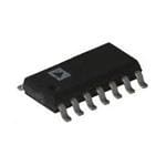
a High Current Output, Triple Video Amplifier AD8023 FEATURES PIN CONFIGURATION Drives 13 V Output 14-Lead SOIC Drives Unlimited Capacitive Load High Current Output Drive: 70 mA Excellent Video Specifications (R = 150 (cid:1)) DISABLE 1 1 14 OUT 2 L Gain Flatness 0.1 dB to 10 MHz DISABLE 2 2 13 –IN 2 0.06% Differential Gain Error DISABLE 3 3 12 +IN 2 0.02(cid:2) Differential Phase Error +VS 4 AD8023 11 –VS Power Operates on (cid:3)2.5 V to (cid:3)7.5 V Supply +IN 1 5 10 +IN 3 10.0mA/Amplifier Max Power Supply Current –IN 1 6 9 –IN 3 High Speed OUT 1 7 8 OUT 3 250 MHz Unity Gain Bandwidth (3 dB) 1200 V/(cid:4)s Slew Rate Fast Settling Time of 35ns (0.1%) High Speed Disable Function The AD8023 uses maximum supply current of 10.0 mA per Turn-Off Time 30 ns amplifier and runs on ±2.5V to ±7.5V power supply. The Easy to Use outputs of each amplifier swing to within one volt of either 200 mA Short Circuit Current supply rail to easily accommodate video signals. The AD8023 Output Swing to 1 V of Rails is unique among current feedback op amps by virtue of its large APPLICATIONS capacitive load drive with a small series resistor, while still LCD Displays achieving rapid settling time. For instance, it can settle to 0.1% in Video Line Driver 35 ns while driving 300 pF capacitance. Broadcast and Professional Video The bandwidth of 250 MHz along with a 1200V/µs slew rate Computer Video Plug-In Boards make the AD8023 useful in high speed applications requiring Consumer Video a single +5 V or dual power supplies up to ±7.5 V. Further- RGB Amplifier in Component Systems more, the AD8023 contains a high speed disable function for PRODUCT DESCRIPTION each amplifier in order to power down the amplifier or high The AD8023 is a high current output drive, high voltage output impedance the output. This can then be used in video multi- drive, triple video amplifier. Each amplifier has 70 mA of output plexing applications. The AD8023 is available in the indus- current and is optimized for driving large capacitive loads. The trial temperature range of –40°C to +85°C. amplifiers are current feedback amplifiers and feature gain flatness of 0.1dB to 10 MHz while offering differential gain and phase error of 0.06% and 0.02°. VIN VIN V V O O Figure 1.Pulse Response Driving a Large Load Capacitor, Figure 2.Output Swing Voltage, CL = 300 pF, G = +3, RF = 750 Ω, RS = 16.9 Ω, RL = 10 kΩ RL = 150Ω; VS = ±7.5 V, G = +10 REV. A Information furnished by Analog Devices is believed to be accurate and reliable. However, no responsibility is assumed by Analog Devices for its use, nor for any infringements of patents or other rights of third parties One Technology Way, P.O. Box 9106, Norwood, MA 02062-9106, U.S.A. which may result from its use. No license is granted by implication or Tel: 781/329-4700 World Wide Web Site: http://www.analog.com otherwise under any patent or patent rights of Analog Devices. Fax: 781/326-8703 © Analog Devices, Inc., 2000
AD8023–SPECIFICATIONS (@ T = +25(cid:2)C, V = (cid:3)7.5, C = 10 pF, R = 150 (cid:1), unless otherwise noted) A S LOAD LOAD Model AD8023A Conditions V Min Typ Max Units S DYNAMIC PERFORMANCE Bandwidth (3 dB) R = 750 Ω No Peaking, G = +3 125 MHz FB Bandwidth (0.1 dB) No Peaking, G = +3 7 MHz Slew Rate 5 V Step 1200 V/µs Settling Time to 0.1% 0 V to ±6 V (6 V Step) C = 300 pF LOAD R > 1 kΩ, R = 750 Ω LOAD FB T = +25°C to +70°C, R = 16.9Ω 30 ns A S NOISE/HARMONIC PERFORMANCE Total Harmonic Distortion f = 5 MHz, R = 150 Ω, V = 2 p-p –72 dBc C L O Input Voltage Noise f = 10 kHz 2.0 nV/√Hz Input Current Noise f = 10 kHz (–I ) 14 pA/√Hz IN Differential Gain (R = 150 Ω) f = 3.58 MHz, G = +2, R = 750 Ω 0.06 % L FB Differential Phase (R = 150 Ω) f = 3.58 MHz, G = +2, R = 750 Ω 0.02 Degrees L FB DC PERFORMANCE Input Offset Voltage T to T –5 2 5 mV MIN MAX Offset Drift 2 µV/°C Input Bias Current (–) T to T –45 15 45 µA MIN MAX Input Bias Current (+) T to T –25 5 25 µA MIN MAX Open-Loop Transresistance 67 111 kΩ T to T 50 111 kΩ MIN MAX INPUT CHARACTERISTICS Input Resistance +Input T to T 100 kΩ MIN MAX –Input T to T 75 Ω MIN MAX Input Capacitance 2 pF Input Common-Mode Voltage Range ±6.0 V Common-Mode Rejection Ratio Input Offset Voltage 50 56 dB –Input Current 0.2 µA/V +Input Current 5 µA/V OUTPUT CHARACTERISTICS Output Voltage Swing R = 1 kΩ V –V 0.8 1.0 V L OL EE V –V 0.8 1.0 V CC OH R = 150 Ω V –V 1.0 1.3 V L OL EE V –V 1.0 1.3 V CC OH Output Current 50 70 mA Short-Circuit Current 300 mA Capacitive Load Drive 1000 pF MATCHING CHARACTERISTICS Dynamic Crosstalk G = +2, f = 5 MHz 70 dB DC Input Offset Voltage –5 0.3 5 mV –Input Bias Current –10 3 10 µA POWER SUPPLY Operating Range Single Supply +4.2 +15 V Dual Supply ±2.1 ±7.5 V Quiescent Current/Amplifier 6.2 mA 7.0 10.0 mA T toT MIN MAX Power-Down 1.3 4.0 mA –2– REV. A
AD8023 Model AD8023A Conditions V Min Typ Max Units S POWER SUPPLY (Continued) Power Supply Rejection Ratio V = ±2.5 V to ±7.5 V dB S Input Offset Voltage 54 76 dB –Input Current 0.03 µA/V +Input Current 0.07 µA/V DISABLE CHARACTERISTICS Off Isolation f = 6 MHz –70 dB Off Output Capacitance G = +1 12 pF Turn-On Time 50 ns Turn-Off Time R = 150 Ω 30 ns L Switching Threshold V – V 1.6 V TH EE Specifications subject to change without notice. ABSOLUTE MAXIMUM RATINGS* Maximum Power Dissipation SupplyVoltage . . . . . . . . . . . . . . . . . . . . . . . . . . 15.5 V Total The maximum power that can be safely dissipated by the AD8023 InternalPowerDissipation is limited by the associated rise in junction temperature. The SmallOutline(R) . . . . 1.0Watts (Observe Derating Curves) maximum safe junction temperature for the plastic encapsulated Input Voltage (Common Mode) . . . . . . . . . . . . . . . . . . . .±V parts is determined by the glass transition temperature of the S DifferentialInputVoltage . . . . . . . . . . . . . . . .±3V (Clamped) plastic, about 150°C. Temporarily exceeding this limit may Output Voltage Limit cause a shift in parametric performance due to a change in the Maximum . . . . . . . . . . . . . . . . . . . . . . . . . . . . . . . . . . .+V stresses exerted on the die by the package. Exceeding a junction S Minimum . . . . . . . . . . . . . . . . . . . . . . . . . . . . . . . . . . . .–V temperature of 175°C for an extended period can result in S Output Short Circuit Duration device failure. . . . . . . . . . . . . . . . . . . . .Observe Power Derating Curves While the AD8023 is internally short circuit protected, this may Storage Temperature Range not be enough to guarantee that the maximum junction temper- R Package . . . . . . . . . . . . . . . . . . . . . . . . –65°C to +125°C ature is not exceeded under all conditions. To ensure proper Operating Temperature Range operation, it is important to observe the derating curves. AD8023A . . . . . . . . . . . . . . . . . . . . . . . . . . –40°C to +85°C Lead Temperature Range (Soldering10sec) . . . . . . . . +300°C It must also be noted that in (noninverting) gain configurations (with low values of gain resistor), a high level of input overdrive *Stresses above those listed under Absolute Maximum Ratings may cause perma- can result in a large input error current, which may result in a nent damage to the device. This is a stress rating only; functional operation of the significant power dissipation in the input stage. This power device at these or any other conditions above those indicated in the operational section of this specification is not implied. Exposure to absolute maximum rating must be included when computing the junction temperature rise conditions for extended periods may affect device reliability. due to total internal power. ORDERING GUIDE 2.5 TJ = +150(cid:2)C Temperature Package Package atts Model Range Description Option W N – 2.0 AD8023AR –40°C to +85°C 14-Lead Plastic SOIC R-14 O TI AD8023AR- –40°C to +85°C 13" Tape and Reel R-14 A P ADR8E0E2L3AR- –40°C to +85°C 7" Tape and Reel R-14 R DISSI1.5 14-LEAD SOIC REEL7 WE AD8023ACHIPS –40°C to +85°C Die O P M 1.0 U M XI A M 0.5 –50 –40–30–20 –10 0 10 20 30 40 50 60 70 80 90 AMBIENT TEMPERATURE – (cid:2)C Figure 3.Maximum Power Dissipation vs. Ambient Temperature CAUTION ESD (electrostatic discharge) sensitive device. Electrostatic charges as high as 4000 V readily WARNING! accumulate on the human body and test equipment and can discharge without detection. Although the AD8023 features proprietary ESD protection circuitry, permanent damage may occur on devices subjected to high energy electrostatic discharges. Therefore, proper ESD precautions are recom- ESD SENSITIVE DEVICE mended to avoid performance degradation or loss of functionality. REV. A –3–
AD8023 METALIZATION PHOTO Contact factory for latest dimensions. Dimensions shown in inches and (mm). –IN1 +IN +VS DISABLE 3 DISABLE 2 6 5 4 3 2 DISABLE 1 1 7 OUT 1 0.0634 (1.61) 14 OUT 2 8 OUT 3 –IN 2 13 –IN3 +IN 3 –VS +IN 2 9 10 11 12 0.0713 (1.81) Typical Performance Characteristics 8 14 Volts 7 13 VS = (cid:3)7.5V (cid:3) p GE – 6 – V p-12 E RAN 5 WING 11 G S E VOLTA 43 OLTAGE 190 D V O T M 2 U 8 ON- UTP MM 1 O 7 O C 0 6 2 3 4 5 6 7 8 10 100 1k 10k SUPPLY VOLTAGE – (cid:3)Volts LOAD RESISTANCE – (cid:1) Figure 4.Input Common-Mode Voltage Range vs. Figure 5.Output Voltage Swing vs. Load Resistance Supply Voltage –4– REV. A
AD8023 25 35 TA = +25(cid:2)C 30 A m 20 A PLY CURRENT – 15 (cid:4)AS CURRENT – 221505 –IB OTAL SUP 150 INPUT BI10 +IB T 5 0 01 2 3 4 5 6 7 8 9 –50–40–30–20–10 0 10 20 30 40 50 60 70 80 90 100 SUPPLY VOLTAGE – (cid:3)Volts TEMPERATURE – (cid:2)C Figure 6. Total Supply Current vs. Supply Voltage Figure 9.Input Bias Current vs. Temperature 16 1 TA = +25(cid:2)C 14 p-p mV WING – V12 TAGE – 0 VS = (cid:3)2.5V E S10 NSOW LIONAGD VOL UT VOLTAG 68 RLS W= 1IN5G0(cid:1) UT OFFSET –1 VS = (cid:3)7.5V P P T N U I O 4 2 –2 2 3 4 5 6 7 8 SUPPLY VOLTAGE – (cid:3)Volts –40 –30 –20 –10 0 TE1M0PE2R0ATU30RE 4–0 (cid:2)C50 60 70 80 90 Figure 7. Output Voltage Swing vs. Supply Voltage Figure 10.Input Offset Voltage vs. Temperature 24 VS = (cid:3)7.5V – V 100 G = +2 22 E A C m N UPPLY CURRENT – 112860 VS = (cid:3)2.5V P OUTPUT RESISTA 331.1101 VS =V (cid:3)S 2=.5 (cid:3)V7.5V S O TAL 14 D-LO 0.31 O E T S 12 O L 0.1 C 10 –50–40–30–20–10 0 10 20 30 40 50 60 70 80 90100 1 10 100 300 TEMPERATURE – (cid:2)C FREQUENCY – MHz Figure 8.Total Supply Current vs. Temperature Figure 11.Closed-Loop Output Resistance vs. Frequency REV. A –5–
AD8023 200 200 90 R 80 100 100 B R – I NOISE – d 70 VCM Hz Hz ON VS = (cid:3)7.5V R (cid:1)nV +I NOISE (cid:1)pA CTI 60 R E – E – EJE 50 OIS OIS E R VS = (cid:3)2.5V N N D 40 GE 10 10 NT MO OLTA URRE MON- 30 V C M 20 O V NOISE C 10 0 1 0 1 10 100 200 0.1 1 10 100 FREQUENCY – MHz FREQUENCY – kHz Figure 12.Input Current and Voltage Noise vs. Frequency Figure 15.Common-Mode Rejection vs. Frequency 450 70 VS = (cid:3)7.5V B 60 VS = (cid:3)7.5V (+PSRR) mA – d VS = (cid:3)2.5V (+PSRR) T – 400 ON 50 EN CTI RR SOURCE JE 40 U E T C350 Y R RCUI SINK UPPL 30 ORT CI300 WER S 20 VS = (cid:3)2.5V (–PSRR) SH PO VS = (cid:3)7.5V (–PSRR) 10 250 –50–40–30–20–10 0 10 20 30 40 50 60 70 80 90 100 0 1 10 100 TEMPERATURE – (cid:2)C FREQUENCY – MHz Figure 13.Short Circuit Current vs. Temperature Figure 16.Power Supply Rejection Ratio vs. Frequency 10k 0 G = +1 –10 VS = (cid:3)7.5V VO = 2V p-p (cid:1)CE – 1k GVS = =+ 1(cid:3)7.5V N – dBc ––2300 N O SISTA 100 TORTI –40 PUT RE NIC DIS ––5600 T O OU 10 ARM –70 2ND H –80 3RD –90 1 10 100 200 1 10 100 FREQUENCY – Hz FREQUENCY – MHz Figure 14.Output Resistance vs. Frequency, Figure 17.Harmonic Distortion vs. Frequency, R = 150Ω L Disabled State –6– REV. A
AD8023 100k (cid:1) – E 10k V C IN N A D E P M 1k SI N A R T 100 V O 10 1k 10k 100k 1M 10M 100M 1G FREQUENCY – Hz Figure 18.Open-Loop Transimpedance vs. Frequency Figure 21.Small Signal Pulse Response, Gain = +1, (R = 2 kΩ, R = 150 Ω, V = ±7.5 V) F L S 1600 1600 G = –1 1400 1400 G = –1 G = +2 G = +2 1200 1200 (cid:4)V/s 1000 G = +1 (cid:4)– V/s 1000 RATE 800 G = +10 RATE 800 G = +1 W W SLE 600 SLE 600 G = +10 400 400 200 200 0 0 2 3 4 5 6 7 8 0 1 2 3 4 5 6 SUPPLY VOLTAGE – V OUTPUT VOLTAGE STEP – V p-p Figure 19.Slew Rate vs. Output Step Size Figure 22.Maximum Slew Rate vs. Supply Voltage V V IN IN V O V O Figure 20.Large Signal Pulse Response, Figure 23.Large Signal Pulse Response, Gain = +1, (RF = 2 kΩ, RL = 150 Ω, VS = ±7.5 V) Gain = +10, (RF = 274 Ω, RL = 150 Ω, VS = ±7.5 V) REV. A –7–
AD8023 +2 +1 ORMALIZED) – dB –+–0121 GAIN VS = (cid:3)2.5VVS = (cid:3)7.5V ORMALIZED) – dB –––0231 GAIN VS = (cid:3)2.5V VS = (cid:3)7.5V CLOSED-LOOP GAIN (N –––––35674 GRPL H= = A+ 1S150E0(cid:1) VS = V(cid:3)S7 =.5 (cid:3)V2.5V ––091080 HASE SHIFT – Degrees CLOSED-LOOP GAIN (N –––––84567 GRPHL = A= + S11E50(cid:1) VS = (cid:3)2V.5SV = (cid:3)7.5V –0–91080ASE SHIFT – Degrees P H –8 –9 P 1 10 100 500 1 10 100 500 FREQUENCY – MHz FREQUENCY – MHz Figure 24.Closed-Loop Gain and Phase vs. Frequency, Figure 27.Closed-Loop Gain and Phase vs. Frequency, G = +10, R = 150 Ω G = –1, R = 150 Ω L L +1 dB 0 D) – –1 GAIN E Z LI –2 A M OR –3 VS = (cid:3)2.5V VIN N N ( –4 VS = (cid:3)7.5V 0 s P GAI –5 PHASE egree O D SED-LO ––67 –90 SHIFT – CLO –8 –180 ASE VO H P –9 1 10 100 400 FREQUENCY – MHz Figure 25.Closed-Loop Gain and Phase vs. Frequency, Figure 28.Small Signal Pulse Response, G = +1, R = 150 Ω Gain = +10, (R = 274 Ω, R = 150 Ω, V = ±7.5 V) L F L S VIN VIN V O V O Figure 26.Large Signal Pulse Response, Figure 29.Small Signal Pulse Response, Gain = –1, (R = 750 Ω, R = 150 Ω, V = ±7.5 V) Gain = –1, (R = 750 Ω, R = 150 Ω, V = ±7.5 V) F L S F L S –8– REV. A
AD8023 +1 G ED) – dB –01 GAIN where: CT = traAnCscLa (cid:2)pa 1c i+taSnCceT (cid:3)(R 1F p+FGnrin) LIZ –2 VS = (cid:3)7.5V RF = feedback resistor MA G = ideal closed loop gain P GAIN (NOR –––453 PHASE VS = (cid:3)2.5V 0 egrees Grinn == i n1v+erRtRinGFg i n=p unto irsees igsatainnce (cid:3) 150 Ω O D CLOSED-LO ––––8679 GRL = = – 11500(cid:1) VS = (cid:3)2.5V ––91080PHASE SHIFT – The –3 dBA bCaLnd =w icdfl3ot hs(cid:2)e ids2 dloπeotCeprT mg(aRiinnF1ed+ fGronmr itnh)is model as: 1 10 100 500 This model will predict –3 dB bandwidth to within about FREQUENCY – MHz 10% to 15% of the correct value when the load is 150 Ω and Figure 30.Closed-Loop Gain and Phase vs. Frequency, V = ±7.5V. For lower supply voltages there will be a slight G = –10, R = 150 Ω S L decrease in bandwidth. The model is not accurate enough to General predict either the phase behavior or the frequency response The AD8023 is a wide bandwidth, triple video amplifier that peaking of the AD8023. offers a high level of performance on less than 9.0 mA per It should be noted that the bandwidth is affected by attenuation amplifier of quiescent supply current. The AD8023 achieves due to the finite input resistance. Also, the open-loop output bandwidth in excess of 200MHz, with low differential gain and resistance of about 6 Ω reduces the bandwidth somewhat when phase errors and high output current making it an efficient video driving load resistors less than about 150 Ω. (Bandwidths will amplifier. be about 10% greater for load resistances above a couple The AD8023’s wide phase margin coupled with a high output hundred ohms.) short circuit current make it an excellent choice when driving any capacitive load up to 300 pF. Table I. –3 dB Bandwidth vs. Closed-Loop Gain and Feedback Resistor, R = 150 (cid:1) (SOIC) It is designed to offer outstanding functionality and performance L at closed-loop inverting or noninverting gains of one or greater. V – Volts Gain R – Ohms BW – MHz S F Choice of Feedback and Gain Resistors ±7.5 +1 2000 460 Because it is a current feedback amplifier, the closed-loop band- +2 750 240 width of the AD8023 may be customized using different values +10 300 50 –1 750 150 of the feedback resistor. Table I shows typical bandwidths at –10 250 60 different supply voltages for some useful closed-loop gains when driving a load of 150 Ω. ±2.5 +1 2000 250 +2 1000 90 The choice of feedback resistor is not critical unless it is desired +10 300 30 to maintain the widest, flattest frequency response. The resistors –1 750 95 recommended in the table (chip resistors) are those that will –10 250 50 result in the widest 0.1 dB bandwidth without peaking. In Driving Capacitive Loads applications requiring the best control of bandwidth, 1% When used in combination with the appropriate feedback resistors are adequate. Resistor values and widest bandwidth resistor, the AD8023 will drive any load capacitance without figures are shown. Wider bandwidths than those in the table can oscillation. The general rule for current feedback amplifiers is be attained by reducing the magnitude of the feedback resistor that the higher the load capacitance, the higher the feedback (at the expense of increased peaking), while peaking can be resistor required for stable operation. Due to the high open-loop reduced by increasing the magnitude of the feedback resistor. transresistance and low inverting input current of the AD8023, Increasing the feedback resistor is especially useful when driving the use of a large feedback resistor does not result in large closed- large capacitive loads as it will increase the phase margin of the loop gain errors. Additionally, its high output short circuit current closed-loop circuit. (Refer to the Driving Capacitive Loads makes possible rapid voltage slewing on large load capacitors. section for more information.) For the best combination of wide bandwidth and clean pulse To estimate the –3 dB bandwidth for closed-loop gains of 2 or response, a small output series resistor is also recommended. greater, for feedback resistors not listed in the following table, Table II contains values of feedback and series resistors which the following single pole model for the AD8023 may be used: result in the best pulse responses. Figure 28 shows the AD8023 driving a 300pF capacitor through a large voltage step with virtually no overshoot. (In this case, the large and small signal pulse responses are quite similar in appearance.) REV. A –9–
AD8023 RF +VS 1.0(cid:4)F 0.1(cid:4)F RG VIN 4 15(cid:1) VIN AD801123 1.0(cid:4)F RS CL VO RT 0.1(cid:4)F –VS V Figure 31.Circuit for Driving a Capacitive Load O Table II. Recommended Feedback and Series Resistors vs. Capacitive Load and Gain Figure 33.50% Overload Recovery, Gain = +10, (R = 300 Ω, R = 1 kΩ, V = ±7.5 V) R – Ohms F L S S C – pF R – Ohms G = 2 G ≥ 3 As noted in the warning under Maximum Power Dissipation, a L F high level of input overdrive in a high noninverting gain circuit 20 2k 0 0 can result in a large current flow in the input stage. Though this 50 2k 10 10 100 2k 15 15 current is internally limited to about 30 mA, its effect on the 200 3k 10 10 total power dissipation may be significant. 300 3k 10 10 Disable Mode Operation ≥500 3k 10 10 Pulling the voltage on any one of the Disable pins about 1.6V up from the negative supply will put the corresponding amplifier into a disabled, powered down, state. In this condition, the amplifier’s quiescent current drops to about 1.3 mA, its output becomes a high impedance, and there is a high level of isolation from input to output. In the case of a gain of two line driver for example, the impedance at the output node will be about the same as for a 1.5 kΩ resistor (the feedback plus gain resistors) in parallel with a 12 pF capacitor. V IN Leaving the Disable pin disconnected (floating) will leave the corresponding amplifier operational, in the enabled state. The input impedance of the disable pin is about 25 kΩ in parallel with a few picofarads. When driven to 0 V, with the negative supply at –7.5 V, about 100 µA flows into the disable pin. V O When the disable pins are driven by complementary output CMOS logic, on a single 5 V supply, the disable and enable times are about 50 ns. When operated on dual supplies, level Figure 32.Pulse Response Driving a Large Load Capacitor. shifting will be required from standard logic outputs to the C = 300 pF, G = +3, R = 750 Ω, R = 16.9 Ω, R = 10 kΩ Disable pins. Figure 33 shows one possible method, which L F S L results in a negligible increase in switching time. Overload Recovery The three important overload conditions are: input common- +5 mode voltage overdrive, output voltage overdrive, and input current overdrive. When configured for a low closed-loop gain, VI +7.5V this amplifier will quickly recover from an input common-mode 15k(cid:1) voltage overdrive; typically in under 25 ns. When configured for a higher gain, and overloaded at the output, the recovery time TO DISABLE PIN will also be short. For example, in a gain of +10, with 50% 4k(cid:1) 10k(cid:1) overdrive, the recovery time of the AD8023 is about 20 ns (see –7.5V Figure 31). For higher overdrive, the response is somewhat VI HIGH => AMPLIFIER ENABLED slower. For 100% overdrive, (in a gain of +10), the recovery VI LOW => AMPLIFIER DISABLED time is about 80 ns. Figure 34.Level Shifting to Drive Disable Pins on Dual Supplies The AD8023’s input stages include protection from the large differential input voltages that may be applied when disabled. Internal clamps limit this voltage to about ±3 V. The high input to output isolation will be maintained for voltages below this limit. –10– REV. A
AD8023 OUTLINE DIMENSIONS Dimensions shown in inches and (mm). 14-Lead Plastic SOIC (R-14) A) 00..33434647 ((88..7555)) ev. 0 (r 14 8 0 0.1574 (4.00) 0.2440 (6.20) 3/ 0.1497 (3.80) 1 7 0.2284 (5.80) 0– – 7 3 1 PIN 1 0.0688 (1.75) 0.0196 (0.50)x 45° C3 0.0098 (0.25) 0.0532 (1.35) 0.0099 (0.25) 0.0040 (0.10) 8° SEPALTAINNGE 0(B1.0.S25C70)0 00..00119328 ((00..4395)) 00..00009795 ((00..2159)) 0° 00..00510600 ((10..2471)) A. S. U. N D I E T N RI P REV. A –11–
Mouser Electronics Authorized Distributor Click to View Pricing, Inventory, Delivery & Lifecycle Information: A nalog Devices Inc.: AD8023AR-EBZ AD8023ARZ AD8023ARZ-REEL AD8023ARZ-REEL7