ICGOO在线商城 > 集成电路(IC) > 线性 - 放大器 - 视频放大器和频缓冲器 > THS7314D
 Datasheet下载
- 型号: THS7314D
- 制造商: Texas Instruments
- 库位|库存: xxxx|xxxx
- 要求:
| 数量阶梯 | 香港交货 | 国内含税 |
| +xxxx | $xxxx | ¥xxxx |
查看当月历史价格
查看今年历史价格
THS7314D产品简介:
ICGOO电子元器件商城为您提供THS7314D由Texas Instruments设计生产,在icgoo商城现货销售,并且可以通过原厂、代理商等渠道进行代购。 THS7314D价格参考¥1.84-¥4.54。Texas InstrumentsTHS7314D封装/规格:线性 - 放大器 - 视频放大器和频缓冲器, Video Amp, 3 Buffer 8-SOIC。您可以下载THS7314D参考资料、Datasheet数据手册功能说明书,资料中有THS7314D 详细功能的应用电路图电压和使用方法及教程。
THS7314D 是由 Texas Instruments 生产的一款高性能视频放大器,广泛应用于需要处理和传输高质量视频信号的场景。以下是该型号的主要应用场景:

 1. 高清视频传输
   THS7314D 支持高达 165 MHz 的带宽,能够处理高分辨率视频信号,如 HD (720p/1080i) 和 Full HD (1080p)。它适用于各种高清视频设备,如监视器、投影仪、电视等,确保视频信号在传输过程中保持清晰度和稳定性。

 2. 视频分配与切换
   在多路视频信号分配和切换系统中,THS7314D 可以作为缓冲器或放大器,确保信号在多个输出端口之间无损传输。它能够有效防止信号衰减和干扰,适用于矩阵切换器、视频分配器等设备。

 3. 安防监控系统
   THS7314D 在安防监控领域有广泛应用,特别是在需要长距离传输视频信号的情况下。它可以增强信号强度,减少噪声和失真,确保监控画面的清晰度和实时性。常见的应用包括闭路电视 (CCTV) 系统、安防摄像头等。

 4. 医疗成像设备
   医疗成像设备如超声波机、内窥镜等对图像质量要求极高。THS7314D 能够提供稳定的信号放大和缓冲功能,确保图像传输的准确性和清晰度,帮助医生进行更精确的诊断。

 5. 工业自动化与机器视觉
   在工业自动化和机器视觉系统中,THS7314D 可用于处理来自摄像头或其他传感器的视频信号,确保图像数据的完整性和准确性。它可以帮助提高生产线的效率和产品质量检测的精度。

 6. 消费电子设备
   THS7314D 还可以应用于各种消费电子产品,如蓝光播放器、游戏机、家庭影院系统等。它能够提升视频信号的质量,提供更好的视听体验。

 总结
THS7314D 凭借其高带宽、低噪声和卓越的信号处理能力,适用于多种需要高质量视频信号传输和处理的场景。无论是专业级的应用还是消费级的产品,THS7314D 都能提供可靠的性能支持。
| 参数 | 数值 |
| -3db带宽 | - |
| 3dB带宽 | 8.5 MHz |
| 产品目录 | 集成电路 (IC)半导体 |
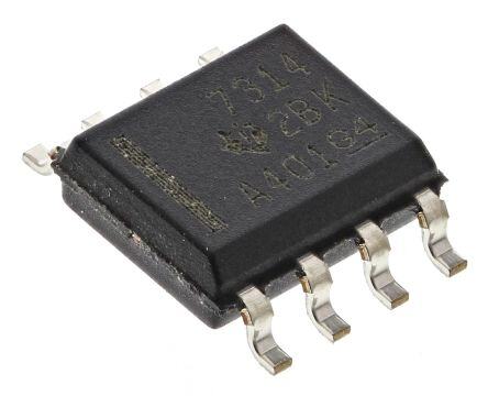
| 描述 | IC SDTV VIDEO AMP 3CH LP 8-SOIC视频放大器 3-Channel SDTV Video Amp |
| DevelopmentKit | THS7314EVM |
| 产品分类 | |
| 品牌 | Texas Instruments |
| 产品手册 | http://www.ti.com/litv/slos513a |
| 产品图片 |
|
| rohs | 符合RoHS无铅 / 符合限制有害物质指令(RoHS)规范要求 |
| 产品系列 | 放大器 IC,视频放大器,Texas Instruments THS7314D- |
| 数据手册 | |
| 产品型号 | THS7314D |
| 产品目录页面 | |
| 产品种类 | 视频放大器 |
| 供应商器件封装 | 8-SOIC |
| 其它名称 | 296-21415-5 |
| 制造商产品页 | http://www.ti.com/general/docs/suppproductinfo.tsp?distId=10&orderablePartNumber=THS7314D |
| 包装 | 管件 |
| 单位重量 | 76 mg |
| 压摆率 | - |
| 商标 | Texas Instruments |
| 安装类型 | 表面贴装 |
| 安装风格 | SMD/SMT |
| 封装 | Tube |
| 封装/外壳 | 8-SOIC(0.154",3.90mm 宽) |
| 封装/箱体 | SOIC-8 |
| 工作温度范围 | - 40 C to + 85 C |
| 工作电源电压 | 2.85 V to 5.5 V |
| 工厂包装数量 | 75 |
| 应用 | 缓冲器 |
| 最大工作温度 | + 85 C |
| 最小工作温度 | - 40 C |
| 标准包装 | 75 |
| 电压-电源,单/双 (±) | 2.85 V ~ 5.5 V |
| 电流-电源 | 16mA |
| 电流-输出/通道 | 70mA |
| 电源电压-最大 | 5.5 V |
| 电源电压-最小 | 2.85 V |
| 电源电流 | 16 mA |
| 电源类型 | Single |
| 电路数 | 3 |
| 系列 | THS7314 |
| 输出类型 | 满摆幅 |
| 通道数量 | 3 Channel |
| 配用 | /product-detail/zh/THS7314EVM/296-31014-ND/1905367 |


- 商务部:美国ITC正式对集成电路等产品启动337调查
- 曝三星4nm工艺存在良率问题 高通将骁龙8 Gen1或转产台积电
- 太阳诱电将投资9.5亿元在常州建新厂生产MLCC 预计2023年完工
- 英特尔发布欧洲新工厂建设计划 深化IDM 2.0 战略
- 台积电先进制程称霸业界 有大客户加持明年业绩稳了
- 达到5530亿美元!SIA预计今年全球半导体销售额将创下新高
- 英特尔拟将自动驾驶子公司Mobileye上市 估值或超500亿美元
- 三星加码芯片和SET,合并消费电子和移动部门,撤换高东真等 CEO
- 三星电子宣布重大人事变动 还合并消费电子和移动部门
- 海关总署:前11个月进口集成电路产品价值2.52万亿元 增长14.8%


PDF Datasheet 数据手册内容提取
THS7314 www.ti.com SLOS513A–DECEMBER2006–REVISEDMARCH2011 th 3-Channel SDTV Video Amplifier With 5 -Order Filters and 6-dB Gain CheckforSamples:THS7314 FEATURES 1 DESCRIPTION • 3SDTVVideoAmplifiersforCVBS,S-Video, Y'P'BP'R480i/576i,Y'U'V',orG'B'R'(R'G'B') Fabricated using the Silicon-Germanium (SiGe) • IntegratedLow-PassFilters BiCom-III process, the THS7314 is a low power – 5th-Order8.5-MHz(–3dB)Butterworth single-supply 3-V to 5-V 3-channel integrated video buffer. It incorporates a 5th-order Butterworth filter – –1dBPassbandBandwidthat7-MHz which is useful as a DAC reconstruction filter or an – 47dBAttenuationat27-MHz ADC anti-aliasing filter. The 8.5-MHz filter is a perfect choice for SDTV video which includes Composite • VersatileInputBiasing (CVBS), S-Video, Y'U'V', G'B'R' (R'G'B'), and Y'P' P' – DC-CoupledWith285-mVOutputShift B R 480i/576i. – AC-CoupledwithSync-TipClamp As part of the THS7314 flexibility, the input can be – AllowsAC-CoupledWithDC-Biasing configured for ac or dc coupled inputs. The 285-mV • Built-in6dBGain(2V/V) output level shift to allow for a full sync dynamic range at the output with 0-V input. The AC coupled • 3-Vto5-VSingleSupplyOperation modes include a transparent sync-tip clamp option for • Rail-to-RailOutput: CVBS, Y', and G'B'R' signals with sync. AC-coupled – OutputSwingsWithin100-mVFromthe biasing for C'/P' /P' channels is achieved by adding B R RailsAllowingACorDCOutputCoupling anexternalresistortoVs+. – AbletoDriveupto2VideoLines – 75Ω The THS7314 is the perfect choice for all output • Low16-mAat3.3-VTotalQuiscentCurrent buffer applications. Its rail-to-rail output stage with 6-dB gain allows for both ac and dc line driving. The • LowDifferentialGain/Phaseof0.1%/0.1° ability to drive 2-lines, or 75-Ω loads, allows for • SOIC-8Package maximum flexibility as a video line driver. The 16-mA total quiescent current at 3.3-V makes it an excellent APPLICATIONS choice for USB powered, portable, or other power • SetTopBoxOutputVideoBuffering sensitivevideoapplications. • PVR/DVDROutputBuffering The THS7314 is available in a small SOIC-8 package • USB/PortableLowPowerVideoBuffering thatisRoHScompliant. 3.3 V CVBS Out 75W DAC/ CVBS Encoder THS7314 R 75W (THS8200) 1 CH.1 IN CH.1 OUT 8 75W SDTV Y’ CVBS Y’ 2 CH.2 IN CH.2 OUT 7 Out S-VideoY’ S-Video C’ R 3 CH.3 IN CH.3 OUT 6 S-Video 480i/576i 4 VS+ GND 5 Y’P’ P’ B R C’ G’B’R’ C’ 75W 75W R 3.3 V 75W Out Figure1. 3.3-VSingle-SupplyDC-Input/DCOutputCoupledVideoLineDriver 1 Pleasebeawarethatanimportantnoticeconcerningavailability,standardwarranty,anduseincriticalapplicationsofTexas Instrumentssemiconductorproductsanddisclaimerstheretoappearsattheendofthisdatasheet. PRODUCTIONDATAinformationiscurrentasofpublicationdate. ©2006–2011,TexasInstrumentsIncorporated Products conform to specifications per the terms of the Texas Instruments standard warranty. Production processing does not necessarilyincludetestingofallparameters.
THS7314 SLOS513A–DECEMBER2006–REVISEDMARCH2011 www.ti.com This integrated circuit can be damaged by ESD. Texas Instruments recommends that all integrated circuits be handled with appropriateprecautions.Failuretoobserveproperhandlingandinstallationprocedurescancausedamage. ESDdamagecanrangefromsubtleperformancedegradationtocompletedevicefailure.Precisionintegratedcircuitsmaybemore susceptibletodamagebecauseverysmallparametricchangescouldcausethedevicenottomeetitspublishedspecifications. PACKAGING/ORDERINGINFORMATION PACKAGEDDEVICES PACKAGETYPE(1) TRANSPORTMEDIA,QUANTITY THS7314D Rails,75 SOIC-8 THS7314DR TapeandReel,2500 (1) Forthemostcurrentpackageandorderinginformation,seethePackageOptionAddendumattheendofthisdocument,orseetheTI websiteatwww.ti.com. ABSOLUTE MAXIMUM RATINGS overoperatingfree-airtemperaturerange(unlessotherwisenoted) (1) VALUE UNIT Supplyvoltage,V toGND 5.5 V S+ V Inputvoltage –0.4VtoV I S+ I Outputcurrent 90 mA O Continuouspowerdissipation SeeDissipationRatingTable T Maximumjunctiontemperature,anycondition(2) 150 °C J T Maximumjunctiontemperature,continuousoperation,longtermreliability(3) 125 °C J T Storagetemperaturerange –65to150 °C stg HBM 2000 ESDratings CDM 1500 V MM 200 (1) Stressesabovethoselistedunderabsolutemaximumratingsmaycausepermanentdamagetothedevice.Thesearestressratings onlyandfunctionaloperationofthedeviceattheseoranyotherconditionsbeyondthoseindicatedunderrecommendedoperating conditionsisnotimplied.Exposuretoabsolutemaximumratedconditionsforextendedperiodsmaydegradedevicereliability. (2) Theabsolutemaximumjunctiontemperatureunderanyconditionislimitedbytheconstraintsofthesiliconprocess. (3) Theabsolutemaximumjunctiontemperatureforcontinuousoperationislimitedbythepackageconstraints.Operationabovethis temperaturemayresultinreducedreliabilityand/orlifetimeofthedevice. DISSIPATION RATINGS POWERRATING(1) PACKAGE θJC θJA (TJ=125°C) (°C/W) (°C/W) T =25°C T =85°C A A SOIC-8(D) 50 130(2) 769mW 308mW (1) Powerratingisdeterminedwithajunctiontemperatureof125°C.Thisisthepointwhereperformancestartstodegradeandlong-term reliabilitystartstobereduced.ThermalmanagementofthefinalPCBshouldstrivetokeepthejunctiontemperatureatorbelow125°C forbestperformanceandreliability. (2) ThisdatawastakenwiththeJEDECHigh-KtestPCB.FortheJEDEClow-KtestPCB,theθ is196°C/W. JA RECOMMENDED OPERATING CONDITIONS MIN MAX UNIT V Supplyvoltage 3 5 V S+ T Ambienttemperature –40 85 °C A 2 SubmitDocumentationFeedback ©2006–2011,TexasInstrumentsIncorporated ProductFolderLink(s):THS7314
THS7314 www.ti.com SLOS513A–DECEMBER2006–REVISEDMARCH2011 FUNCTIONALDIAGRAM +Vs + Level gm - Shift Channel 1 6dB Channel 1 Input Sync-Tip LPF Output 800 kW Clamp 5-Pole (DC Restore) 8.5-MHz +Vs gm+ Level - Shift Channel 2 6dB Channel 2 LPF Input Sync-Tip Output 800 kW Clamp 5-Pole (DC Restore) 8.5-MHz +Vs gm+ Level - Shift Channel 3 6dB Channel 3 LPF Input Sync-Tip Output 800 kW Clamp 5-Pole (DC Restore) 8.5-MHz 3 V to 5 V PIN CONFIGURATION SOIC-8(D) (TOPVIEW) THS7314 CH.1 IN 1 8 CH.1 OUT CH.2 IN 2 7 CH.2 OUT CH.3 IN 3 6 CH.3 OUT V 4 5 GND S+ PINFUNCTIONS PIN I/O DESCRIPTION NAME NO.SOIC-8 CH.1–INPUT 1 I VideoInput–Channel1 CH.2–INPUT 2 I VideoInput–Channel2 CH.3–INPUT 3 I VideoInput–Channel3 +Vs 4 I PositivePowerSupplyPin–connectto3Vto5V. GND 5 I GroundPinforallinternalcircuitry. CH.3–OUTPUT 6 O VideoOutput–Channel3 CH.2–OUTPUT 7 O VideoOutput–Channel2 CH.1–OUTPUT 8 O VideoOutput–Channel1 ©2006–2011,TexasInstrumentsIncorporated SubmitDocumentationFeedback 3 ProductFolderLink(s):THS7314
THS7314 SLOS513A–DECEMBER2006–REVISEDMARCH2011 www.ti.com ELECTRICAL CHARACTERISTICS V = 3.3 V: S+ R =150ΩtoGND–ReferenceFigure2andFigure3(unlessotherwisenoted) L TYP OVERTEMPERATURE PARAMETER TESTCONDITIONS 0°Cto –40°Cto MIN/ 25°C 25°C UNITS 70°C 85°C MAX ACPERFORMANCE Small-signalbandwidth(–3dB) VO –0.2VPP(1) 8.5 6.7/10.3 6.6/10.5 6.5/10.6 MHz Min/Max Large-signalbandwidth(–3dB) VO –2VPP(1) 8.5 6.7/10.3 6.6/10.5 6.5/10.6 MHz Min/Max –1dBPassbandbandwidth 7 MHz Typ Attenuation f=6MHz(2) 0.45 –0.3/2.4 –0.35/2.5 –0.4/2.6 dB Min/Max Withrespectto100kHz f=27MHz(2) 47 36 35 34 dB Min Groupdelay f=100kHz 57 ns Typ Groupdelayvariation f=5.1MHz 10.2 ns Typ withrespectto100kHz Channel-to-channeldelay 0.3 ns Typ Differentialgain NTSC/PAL 0.1/0.1 % Typ Differentialphase NTSC/PAL 0.1/0.1 ° Typ Totalharmonicdistortion f=1MHz;VO=2VPP;ACcoupledI/O –66 dB Typ Signaltonoiseratio NTC-7Weighting,100kHzto4.2MHz 79.6 dB Typ Channel-to-channelcrosstalk f=1MHz,WorstCaseChannels –60 dB Typ ACGain–Allchannels 6 5.7/6.3 5.65/6.35 5.65/6.35 dB Min/Max OutputImpedance f=5MHz 0.63 Ω Typ DCPERFORMANCE Biasedoutputvoltage VI=0V 285 210/370 200/380 190/390 mV Min/Max Inputvoltagerange DCinput,limitedbyoutput –0.1/1.46 V Typ Synctipclampchargecurrent VI=–0.1V 180 μA Typ Inputresistance 800 kΩ Typ Inputcapacitance 2 pF Typ OUTPUTCHARACTERISTICS RL=150ΩtoMidrail 3.15 V Typ RL=150ΩtoGND 3.1 2.85 2.75 2.75 V Min Highoutputvoltageswing RL=75ΩtoMidrail 3.1 V Typ RL=75ΩtoGND 3 V Typ RL=150ΩtoMidrail(VI=–0.2V) 0.15 V Typ RL=150ΩtoGND(VI=–0.2V) 0.1 0.17 0.2 0.21 V Max Lowoutputvoltageswing RL=75ΩtoMidrail(VI=–0.2V) 0.3 V Typ RL=75ΩtoGND(VI=–0.2V) 0.1 V Typ Outputcurrent(sourcing) RL=10ΩtoMidrail 80 mA Typ Outputcurrent(sinking) RL=10ΩtoMidrail 70 mA Typ POWERSUPPLY Maximumoperatingvoltage See(1) 3.3 5.5 5.5 5.5 V Max Minimumoperatingvoltage See(1) 3.3 2.85 2.85 2.85 V Min Maximumquiescentcurrent VI=0V 16 20 22 24 mA Max Minimumquiescentcurrent VI=0V 16 12 11.6 11 mA Min PowerSupplyRejection(+PSRR) 52 dB Typ (1) TheMin/Maxvalueslistedforthisspecificationarespecifiedbydesignandcharacterizationonly. (2) 3.3-VSupplyFilterspecificationsarespecifiedby100%testingat5-Vsupplyalongwithdesignandcharacterizationonly. 4 SubmitDocumentationFeedback ©2006–2011,TexasInstrumentsIncorporated ProductFolderLink(s):THS7314
THS7314 www.ti.com SLOS513A–DECEMBER2006–REVISEDMARCH2011 ELECTRICAL CHARACTERISTICS V = 5 V: S+ R =150ΩtoGND–ReferenceFigure2andFigure3(unlessotherwisenoted) L TYP OVERTEMPERATURE PARAMETER TESTCONDITIONS 0°Cto –40°Cto MIN/ 25°C 25°C UNITS 70°C 85°C MAX ACPERFORMANCE Small-signalbandwidth(–3dB) VO–0.2VPP(1) 8.5 6.7/10.3 6.6/10.5 6.5/10.6 MHz Min/Max Large-signalbandwidth(–3dB) VO–2VPP(1) 8.5 6.7/10.3 6.6/10.5 6.5/10.6 MHz Min/Max –1dBPassbandbandwidth 7 MHz Typ Attenuation f=6MHz 0.45 –0.3/2.4 –0.35/2.5 –0.4/2.6 dB Min/Max Withrespectto100kHz f=27MHz 47 36 35 34 dB Min Groupdelay f=100kHz 57 ns Typ Groupdelayvariation f=5.1MHz 10 ns Typ withrespectto100kHz Channel-to-channeldelay 0.3 ns Typ Differentialgain NTSC/PAL 0.1/0.1 % Typ Differentialphase NTSC/PAL 0.1/0.1 ° Typ Totalharmonicdistortion f=1MHz;VO=2VPP –66 dB Typ Signaltonoiseratio NTC-7Weighting,100kHzto4.2MHz 79.6 dB Typ Channel-to-channelcrosstalk f=1MHz,WorstCaseChannels –60 dB Typ ACGain–Allchannels 6 5.7/6.3 5.65/6.35 5.65/6.35 dB Min/Max OutputImpedance f=5MHz 0.62 Ω Typ DCPERFORMANCE Biasedoutputvoltage VI=0V 290 210/370 200/380 190/390 mV Min/Max Inputvoltagerange Limitedbyoutput –0.1/2.3 V Typ Synctipclampchargecurrent VI=–0.1V 180 μA Typ Inputresistance 800 kΩ Typ Inputcapacitance 2 pF Typ OUTPUTCHARACTERISTICS RL=150ΩtoMidrail 4.85 V Typ RL=150ΩtoGND 4.7 4.2 4.1 4.1 V Min Highoutputvoltageswing RL=75ΩtoMidrail 4.7 V Typ RL=75ΩtoGND 4.5 V Typ RL=150ΩtoMidrail(VI=–0.2V) 0.2 V Typ RL=150ΩtoGND(VI=–0.2V) 0.12 0.23 0.26 0.27 V Max Lowoutputvoltageswing RL=75ΩtoMidrail(VI=–0.2V) 0.35 V Typ RL=75ΩtoGND(VI=–0.2V) 0.1 V Typ Outputcurrent(sourcing) RL=10ΩtoMidrail 90 mA Typ Outputcurrent(sinking) RL=10ΩtoMidrail 85 mA Typ POWERSUPPLY Maximumoperatingvoltage See(1) 5 5.5 5.5 5.5 V Max Minimumoperatingvoltage See(1) 5 2.85 2.85 2.85 V Min Maximumquiescentcurrent VI=0V 17 22 24 25 mA Max Minimumquiescentcurrent VI=0V 17 12.5 12 11.5 mA Min PowerSupplyRejection(+PSRR) 55 dB Typ (1) TheMin/Maxvalueslistedforthisspecificationarespecifiedbydesignandcharacterizationonly. ©2006–2011,TexasInstrumentsIncorporated SubmitDocumentationFeedback 5 ProductFolderLink(s):THS7314
THS7314 SLOS513A–DECEMBER2006–REVISEDMARCH2011 www.ti.com DUT RTERM RLOAD 1 CH.1IN CH.1OUT8 2 CH.2IN CH.2OUT7 RSOURCE RTERM 34 VCSH+.3IN CH.3GONUDT56 RLOAD 0.1mF VSOURCE RTERM RLOAD + 100mF +VS Figure2.DCCoupledInputandOutputTestCircuit 470mF CIN + RTERM DUT 0.1mF RLOAD CIN 1 CH.1IN CH.1OUT8 470mF + 2 CH.2IN CH.2OUT7 RSOURCE RTERM CIN 34 VCSH+.3IN CH.3GONUDT56 0.1mF RLOAD 470mF 0.1mF + VSOURCE RTERM + RLOAD 100mF 0.1mF +VS Figure3.ACCoupledInputandOutputTestCircuit 6 SubmitDocumentationFeedback ©2006–2011,TexasInstrumentsIncorporated ProductFolderLink(s):THS7314
THS7314 www.ti.com SLOS513A–DECEMBER2006–REVISEDMARCH2011 TYPICAL CHARACTERISTICS SMALL-SIGNALGAINvsFREQUENCY PHASEvsFREQUENCY 10 45 0 0 B −45 d −10 − −90 n Gai −20 °− −135 Signal −30 RL = 75 W || 13 pF RL = 150 W || 13 pF Phase −180 mall- −40 −225 S −270 VS = 3.3 V −50 VVSO == 32.030 V mVPP −315 VROL == 125000 Wm V|| P1P3 pF −60 −360 0.1 1 10 100 1k 0.1 1 10 100 f − Frequency − MHz f − Frequency − MHz G001 G002 Figure4. Figure5. SMALL-SIGNALGAINvsFREQUENCY GROUPDELAYvsFREQUENCY 6.5 90 85 VS = 3.3 V 6.0 VO = 200 mVPP B 5.5 80 RL = 150 W || 13 pF Gain − d 5.0 RL = 150 W || 13 pF RL = 75 W || 13 pF ay − ns 7705 nal 4.5 Del 65 Sig 4.0 up 60 all- Gro 55 Sm 3.5 50 3.0 VS = 3.3 V VO = 200 mVPP 45 2.5 40 0.1 1 10 0.1 1 10 100 f − Frequency − MHz f − Frequency − MHz G003 G004 Figure6. Figure7. SMALL-SIGNALPULSERESPONSE LARGE-SIGNALPULSERESPONSE vs vs TIME TIME 2.0 0.8 5.0 2.0 InputVoltage Waveforms VS= 3.3 V 4.5 InputVoltage Waveforms VS= 3.3 V 1.5 RL= 150Ω|| 13 pF RL= 150Ω|| 13 pF −Outpuoltage−t VV 111...789 tr/tf= t1r/ tnfs=t r1/tI4fn=0p un1ts40 ns 000...567 −Ioltanput Vge−V −oltagOutput Ve−V 122334......505050 tr/tf= t1r/ tnfst=r/ t1Ifn4=p0 u1 nt4s0 ns −−−001...110050...505 −Inpoltage−ut VV VO 1.6 Input 0.4 VI VO 1.0 Input −2.0 VI tr/tf= 1 ns tr/tf= 1 ns 0.5 −2.5 Output Voltage Waveforms Output Voltage Waveforms 1.5 0.3 0.0 −3.0 −100 0 100 200 300 400 500 600 700 800 900 −100 0 100 200 300 400 500 600 700 800 900 t−Time−ns t−Time−ns G009 G011 Figure8. Figure9. ©2006–2011,TexasInstrumentsIncorporated SubmitDocumentationFeedback 7 ProductFolderLink(s):THS7314
THS7314 SLOS513A–DECEMBER2006–REVISEDMARCH2011 www.ti.com TYPICAL CHARACTERISTICS (continued) HD2vsOUTPUTVOLTAGE HD3vsOUTPUTVOLTAGE −40 −50 B VS = 3.3 V B VS = 3.3 V − d −45 RL = 150 W || 13 pF − d −55 RL = 150 W || 13 pF on −50 f = 2 MHz on −60 orti f = 4 MHz orti nic Dist −−6505 nic Dist −−7605 f = 4 MHz f = 2 MHz o o m m Har −65 Har −75 Order −70 Order −80 2nd −75 f = 1 MHz 3rd −85 f = 1 MHz −80 −90 0.0 0.5 1.0 1.5 2.0 2.5 3.0 0.0 0.5 1.0 1.5 2.0 2.5 3.0 VO − Output Voltage − VPP G013 VO − Output Voltage − VPP G014 Figure10. Figure11. SLEWRATEvsOUTPUTVOLTAGE CROSSTALKvsFREQUENCY 50 −30 45 VRSL == 135.30 VW || 13 pF −40 VVSO == 31. 3V PVP Ch.1 <−> Ch.2 s 40 RL = 150 W || 13 pF mw Rate − V/ 233505 stalk − dB −−6500 Ch.1 <−> Ch.3 R − Sle 1250 Cros −70 S 10 −80 5 Ch.2 <−> Ch.3 0 −90 0.5 1.0 1.5 2.0 2.5 0.1 1 10 100 1k VO − Output Voltage − VPP G017 f − Frequency − MHz G019 Figure12. Figure13. SMALL-SIGNALGAINvsFREQUENCY OUTPUTIMPEDANCEvsFREQUENCY 10 100 VS = 3.3 V 0 Gain−dB −−2100 CL= 5 pF Wedance − 10 Signal −30 CL= 13 pF put Imp Small- −40 VS= 3.3 V CL= 27 pF − OutO 1 −50 VO= 200 mVPP Z RL= 150Ω|| CL −60 0.1 0.1 1 10 100 1k 0.1 1 10 100 f−Frequency−MHz f − Frequency − MHz G021 G023 Figure14. Figure15. 8 SubmitDocumentationFeedback ©2006–2011,TexasInstrumentsIncorporated ProductFolderLink(s):THS7314
THS7314 www.ti.com SLOS513A–DECEMBER2006–REVISEDMARCH2011 TYPICAL CHARACTERISTICS (continued) SMALL-SIGNALGAINvsFREQUENCY PHASEvsFREQUENCY 10 45 0 0 B −45 d −10 − −90 n Gai −20 °− −135 Signal −30 RL = 75 W || 13 pF RL = 150 W || 13 pF Phase −180 mall- −40 −225 S −270 VS = 5 V −50 VVSO == 52 0V0 mVPP −315 VROL == 125000 Wm V|| P1P3 pF −60 −360 0.1 1 10 100 1k 0.1 1 10 100 f − Frequency − MHz f − Frequency − MHz G005 G006 Figure16. Figure17. SMALL-SIGNALGAINvsFREQUENCY GROUPDELAYvsFREQUENCY 6.5 90 85 VS = 5 V 6.0 VO = 200 mVPP B 5.5 80 RL = 150 W || 13 pF Gain − d 5.0 RL = 150 W || 13 pF RL = 75 W || 13 pF ay − ns 7705 nal 4.5 Del 65 Sig 4.0 up 60 all- Gro 55 Sm 3.5 50 3.0 VS = 5 V VO = 200 mVPP 45 2.5 40 0.1 1 10 0.1 1 10 100 f − Frequency − MHz f − Frequency − MHz G007 G008 Figure18. Figure19. SMALL-SIGNALPULSERESPONSE LARGE-SIGNALPULSERESPONSE vs vs TIME TIME 2.8 1.2 6.0 2.5 InputVoltage Waveforms VS= 5 V 5.5 InputVoltage Waveforms VS= 5 V 2.0 RL= 150Ω|| 13 pF RL= 150Ω|| 13 pF oltagput Ve−V 22..67 tr/ttfr=/tf 1= n1s40 ns 11..01 out Vltage−V poltageut V−V 3445....5050 tr/tf= t1r/ tnfs= 140 ns 0011....0505 oltaut Vge−V −Out 2.5 tr/tIfn=p u1t40 ns 0.9 −Inp −Out 23..50 tr/tIfn=p u1t40 ns −−10..05 −Inp VO 2.4 Input 0.8 VI VO 2.0 Input −1.5 VI tr/tf= 1 ns tr/tf= 1 ns 1.5 −2.0 Output Voltage Waveforms Output Voltage Waveforms 2.3 0.7 1.0 −2.5 −100 0 100 200 300 400 500 600 700 800 900 −100 0 100 200 300 400 500 600 700 800 900 t−Time−ns t−Time−ns G010 G012 Figure20. Figure21. ©2006–2011,TexasInstrumentsIncorporated SubmitDocumentationFeedback 9 ProductFolderLink(s):THS7314
THS7314 SLOS513A–DECEMBER2006–REVISEDMARCH2011 www.ti.com TYPICAL CHARACTERISTICS (continued) HD2vsOUTPUTVOLTAGE HD3vsOUTPUTVOLTAGE −40 −50 B VS = 5 V B VS = 5 V − d −45 RL = 150 W || 13 pF − d −55 RL = 150 W || 13 pF n n o −50 o −60 orti f = 4 MHz f = 2 MHz orti Dist −55 Dist −65 f = 2 MHz nic −60 nic −70 f = 4 MHz o o m m Har −65 Har −75 Order −70 Order −80 2nd −75 f = 1 MHz 3rd −85 f = 1 MHz −80 −90 0.0 0.5 1.0 1.5 2.0 2.5 3.0 3.5 4.0 4.5 0.0 0.5 1.0 1.5 2.0 2.5 3.0 3.5 4.0 4.5 VO − Output Voltage − VPP G015 VO − Output Voltage − VPP G016 Figure22. Figure23. SLEWRATEvsOUTPUTVOLTAGE CROSSTALKvsFREQUENCY 70 −30 VS = 5 V VS = 5 V 60 RL = 150 W || 13 pF −40 VO = 1 VPP Ch.1 <−> Ch.2 s RL = 150 W || 13 pF mew Rate − V/ 345000 sstalk − dB −−6500 Ch.1 <−> Ch.3 − Sl Cro −70 R 20 S −80 10 Ch.2 <−> Ch.3 0 −90 0.5 1.0 1.5 2.0 2.5 3.0 3.5 0.1 1 10 100 1k VO − Output Voltage − VPP G018 f − Frequency − MHz G020 Figure24. Figure25. SMALL-SIGNALGAINvsFREQUENCY OUTPUTIMPEDANCEvsFREQUENCY 10 100 VS = 5 V 0 Gain−dB −−2100 CL= 5 pF Wedance − 10 Signal −30 CL= 13 pF put Imp Small- −40 VS= 5 V CL= 27 pF − OutO 1 −50 VO= 200 mVPP Z RL= 150Ω|| CL −60 0.1 0.1 1 10 100 1k 0.1 1 10 100 f−Frequency−MHz f − Frequency − MHz G022 G024 Figure26. Figure27. 10 SubmitDocumentationFeedback ©2006–2011,TexasInstrumentsIncorporated ProductFolderLink(s):THS7314
THS7314 www.ti.com SLOS513A–DECEMBER2006–REVISEDMARCH2011 APPLICATION INFORMATION The THS7314 is targeted for standard definition video output buffer applications. Although it can be used for numerousotherapplications,theneedsandrequirementsofthevideosignalisanimportantdesignparameterof the THS7314. Built on the Silicon Germanium (SiGe) BiCom-3 process, the THS7314 incorporates many featuresnottypicallyfoundinintegratedvideopartswhileconsumingverylowpower. TheTHS7314hasthefollowingfeatures: • Single-Supply3-Vto5-Voperationwithlowtotalquiescentcurrentof16-mAat3.3-Vand17-mAat5-V. • InputconfigurationacceptingDC+Levelshift,ACSync-TipClamp,orAC-Bias. • AC-Biasingisaccomplishedwiththeuseofexternalpull-upresistortothepositivepowersupply. • 5th-OrderLowPassFilterforDACreconstructionorADCimagerejection: – 8.5-MHz for NTSC, PAL, SECAM, Composite (CVBS), S-Video Y'C', 480i/576i Y'P' P' , and G'B'R' B R (R'G'B')signals. • Internal fixed gain of 2 V/V (6 dB) buffer that can drive up to 2 video lines with dc coupling or traditional ac coupling. • Signal flow-through configuration using an 8-pin SOIC package that complies with the latest lead-free (RoHS compatible)andGreenmanufacturingrequirements. OPERATING VOLTAGE The THS7314 is designed to operate from 3-V to 5-V over a –40°C to 85°C temperature range. The impact on performance over the entire temperature range is negligible due to the implementation of thin film resistors and high quality – low temperature coefficient capacitors. The design of the THS7314 allows operation down to 2.85-V, but for best results the use of a 3-V supply or greater should be used to ensure there are no issues with headroomorclipping. The power supply pins should have a 0.1 μF to 0.01 μF capacitor placed as close as possible to these pins. Failure to do so may result in the THS7314 outputs ringing or have an oscillation. Additionally, a large capacitor, such as 22 μF to 100 μF, should be placed on the power supply line to minimize interference with 50/60 Hz line frequencies. INPUT VOLTAGE The THS7314 input range allows for an input signal range from –0.2V to about (V – 1.5V). But, due to the s+ internalfixedgainof2V/V(6dB)andtheinternallevelshiftofnominally145-mV,theoutputwillgenerallybethe limiting factor for the allowable linear input range. For example, with a 5-V supply, the linear input range is from –0.2V to 3.5V. But due to the gain and level shift, the linear output range limits the allowable linear input rangetobefromabout–0.1Vto2.3V. INPUT OVERVOLTAGE PROTECTION The THS7314 is built using a very high-speed complementary bipolar and CMOS process. The internal junction breakdown voltages are relatively low for these very small geometry devices. These breakdowns are reflected in the Absolute Maximum Ratings table. All input and output device pins are protected with internal ESD protection diodestothepowersupplies,asshowninFigure28. ©2006–2011,TexasInstrumentsIncorporated SubmitDocumentationFeedback 11 ProductFolderLink(s):THS7314
THS7314 SLOS513A–DECEMBER2006–REVISEDMARCH2011 www.ti.com +Vs External Input/ Internal Output Circuitry Pin Figure28. InternalESDProtection These diodes provide moderate protection to input overdrive voltages above and below the supplies as well. The protectiondiodescantypicallysupport30-mAofcontinuouscurrentwhenoverdriven. TYPICAL CONFIGURATION and VIDEO TERMINOLOGY A typical application circuit using the THS7314 as a video buffer is shown in Figure 29. It shows a DAC (or encoder such as the THS8200) driving the three input channels of the THS7314. Although the S-Video Y'C' channels and the Composite video channel of a Standard Definition video (SD) system are shown, these channelscaneasilybetheY'P' P' (sometimeslabeledY'U'V'orincorrectlylabeledY'C' C' )signalsofa480ior B R B R 576isystem.ThesesignalscanalsobeG'B'R'(R'G'B')signalsorothervariations. Note that the Y' term is used for the luma channels throughout this document rather than the more common luminance (Y) term. The reason is to account for the definition of luminance as stipulated by the CIE – International Commission on Illumination. Video departs from true luminance since a nonlinear term, gamma, is added to the true RGB signals to form R'G'B' signals. These R'G'B' signals are then used to mathematically createluma(Y').Thusluminance(Y)isnotmaintainedprovidingadifferenceinterminology. This rationale is also used for the chroma (C') term. Chroma is derived from the non-linear R'G'B' terms and thus it is nonlinear. Chominance (C) is derived from linear RGB giving the difference between chroma (C') and chrominance (C). The color difference signals (P' / P' / U' / V') are also referenced this way to denote the B R nonlinear(gammacorrected)signals. R'G'B' (commonly mislabeled RGB) is also called G’B’R’ (again commonly mislabeled as GBR) in professional video systems. The SMPTE component standard stipulates that the luma information is placed on the first channel, the blue color difference is placed on the second channel, and the red color difference signal is placed onthethirdchannel.ThisisconsistentwiththeY'P' P' nomenclature.Becausethelumachannel(Y')carriesthe B R sync information and the green channel (G') also carries the sync information, it makes logical sense that G' be placed first in the system. Since the blue color difference channel (P' ) is next and the red color difference B channel (P' ) is last, then it also makes logical sense to place the B' signal on the second channel and the R' R signal on the third channel respectfully. Thus hardware compatibility is better achieved when using G'B'R' rather than R'G'B'. Note that for many G'B'R' systems sync is embeded on all three channels, but may not always be thecaseinallsystems. 12 SubmitDocumentationFeedback ©2006–2011,TexasInstrumentsIncorporated ProductFolderLink(s):THS7314
THS7314 www.ti.com SLOS513A–DECEMBER2006–REVISEDMARCH2011 3.3 V CVBS 330mF 75W Out + DAC/ CVBS Encoder R THS7314 75W 1 CH.1 IN CH.1 OUT 8 330mF 75W SDTV + Y’ CVBS Y’ 2 CH.2 IN CH.2 OUT 7 Out S-VideoY’ S-Video C’ R 3 CH.3 IN CH.3 OUT 6 S-Video 4Y8’P0’i/5P7’6i 4 VS+ GND 5 0.1mF B R C’ G’B’R’ 0.1mF C’ 75W 75W R 75W Out + 22mF 3 V to 5 V Figure29. TypicalSDTVCVBS/Y'/C' InputsFromDC-CoupledEncoder/DAC WithAC-CoupledLineDriving INPUT MODE OF OPERATION – DC The inputs to the THS7314 allows for both ac-coupled and dc-coupled inputs. Many DACs or Video Encoders can be dc connected to the THS7314. One of the drawbacks to dc coupling is when 0-V is applied to the input. Although the input of the THS7314 allows for a 0-V input signal with no issues, the output swing of a traditional amplifier cannot yield a 0-V signal resulting in possible clipping. This is true for any single-supply amplifier due to the limitations of the output transistors. Both CMOS and bipolar transistors cannot go to 0-V while sinking current. This trait of a transistor is also the same reason why the highest output voltage is always less than the powersupplyvoltagewhensourcingcurrent. This output clipping can reduce the sync amplitudes (both horizontal and vertical sync amplitudes) on the video signal. A problem occurs if the receiver of this video signal uses an AGC loop to account for losses in the transmission line. Some video AGC circuits derive gain from the horizontal sync amplitude. If clipping occurs on the sync amplitude, then the AGC circuit can increase the gain too much – resulting in too much luma and/or chroma amplitude gain correction. This may result in a picture with an overly bright display with too much color saturation. Other AGC circuits use the chroma burst amplitude for amplitude control, and a reduction in the sync signals does not alter the proper gain setting. But, it is good engineering design practice to ensure saturation/clipping does not take place. Transistors always take a finite amount of time to come out of saturation. This saturation couldpossiblyresultintimingdelaysorotheraberrationsonthesignals. To eliminate saturation/clipping problems, the THS7314 has a 145-mV input level shift feature. This feature takes the input voltage and adds an internal +145-mV shift to the signal. Since the THS7314 also has a gain of 6 dB (2 V/V), the resulting output with a 0-V applied input signal is about 290-mV. The THS7314 rail-to-rail output stage can create this output level while connected to a typical video load with AC or DC coupling. This ensures that no saturation / clipping of the sync signals occur. This is a constant shift regardless of the input signal. For example, ifa1-Vinputisapplied,theoutputisat2.29-V. Because the internal gain is fixed at 6 dB, the gain dictates what the allowable linear input voltage range can be without clipping concerns. For example, if the power supply is set to 3-V, the maximum output is about 2.9-V while driving a significant amount of current. Thus, to avoid clipping, the allowable input is ((2.9V / 2) – 0.145V) = 1.305V. This is true for up to the maximum recommended 5-V power supply that allows about a ((4.9V / 2) – 0.145V)=2.305Vinputrangewhileavoidingclippingontheoutput. The input impedance of the THS7314 in this mode of operation is dictated by the internal 800-kΩ pull-down resistor. This is shown in Figure 30. Note that the internal voltage shift does not appear at the input pin, only the outputpin. ©2006–2011,TexasInstrumentsIncorporated SubmitDocumentationFeedback 13 ProductFolderLink(s):THS7314
THS7314 SLOS513A–DECEMBER2006–REVISEDMARCH2011 www.ti.com +Vs Internal Circuitry Input + 800kW - 145mV Level Shifter Figure30. EquivalentDCInputModeCircuit INPUT MODE OF OPERATION – AC SYNC TIP CLAMP Some video DACs or encoders are not referenced to ground but rather to the positive power supply. These DACs typically only sink current rather than the more traditional current sourcing DAC where the resistor is referenced to ground. The resulting video signals can be too high of a voltage for a dc-coupled video buffer to function properly. To account for this scenario the THS7314 incorporates a sync-tip clamp circuit. This function requires a capacitor (nominally 0.1 μF) to be in series with the input. Note that while the term sync-tip-clamp is used throughout this document, it should be noted that the THS7314 is be better termed as a dc-restoration circuit based on how this function is performed. This circuit is an active clamp circuit and not a passive diode clampfunction. The input to the THS7314 has an internal control loop which sets the lowest input applied voltage to clamp at ground (0-V). By setting the reference at 0-V, the THS7314 allows a dc-coupled input to also function. Hence the STC is considered transparent since it does not operate unless the input signal goes below ground. The signal then goes thru the same 145-mV level shifter resulting in an output voltage low level of 290-mV. If the input signal tries to go below the 0-V, the internal control loop of the THS7314 will source up to 3-mA of current to increase the input voltage level on the THS7314 input side of the coupling capacitor. As soon as the voltage goesabovethe0-Vlevel,theloopstopssourcingcurrentandbecomeshighimpedance. One of the concerns about the sync-tip-clamp level is how the clamp reacts to a sync edge that has overshoot—common in VCR signals or reflections found in poor PCB layouts. Ideally the STC should not react to the overshoot voltage of the input signal. Otherwise, this could result in clipping on the rest of the video signal as itmayraisethebiasvoltagetoomuch. To help minimize this input signal overshoot problem, the control loop in the THS7314 has an internal low-pass filter as shown in Figure 31. This filter reduces the response time of the STC circuit. This delay is a function of how far the voltage is below ground, but in general it is about a 100-ns delay. The effect of this filter is to slow downtheresponseofthecontrolloopsoasnottoclampontheinputovershootvoltagebutrathertheflatportion ofthesyncsignal. Asaresultofthisdelay,thesyncmayhaveanapparentvoltageshift.Theamountofshiftisdependantuponthe amount of droop in the signal as dictated by the input capacitor and the STC current flow. Because the sync is primarily for timing purposes with syncing occurring on the edge of the sync signal, this shift is transparent in mostsystems. While this feature may not fully eliminate overshoot issues on the input signal for excessive overshoot and/or ringing, the STC system should help minimize improper clamping levels. As an additional method to help minimize this issue, an external capacitor (ex: 10 pF to 47 pF) to ground in parallel with the external termination resistorscanhelpfilterovershootproblems. It should be noted that this STC system is dynamic and does not rely upon timing in any way. It only depends on the voltage appearing at the input pin at any given point in time. The STC filtering helps minimize level shift problems associated with switching noises or very short spikes on the signal line. This helps ensure a very robustSTCsystem. 14 SubmitDocumentationFeedback ©2006–2011,TexasInstrumentsIncorporated ProductFolderLink(s):THS7314
THS7314 www.ti.com SLOS513A–DECEMBER2006–REVISEDMARCH2011 +Vs +Vs STC LPF Comparator Internal Circuitry + Input - Pin Input + 0.1mF 800kW - 145mV Level Shifter Figure31. EquivalentACSyncTipClampInputCircuit When the AC Sync-Tip-Clamp (STC) operation is used, there must also be some finite amount of discharge bias current. As previously described, if the input signal goes below the 0-V clamp level, the internal loop of the THS7314 will source current to increase the voltage appearing at the input pin. As the difference between the signal level and the 0-V reference level increases, the amount of source current increases proportionally—supplying up to 3 mA of current. Thus the time to re-establish the proper STC voltage can be fast.Ifthedifferenceissmall,thenthesourcecurrentisalsosmalltoaccountforminorvoltagedroop. But, what happens if the input signal goes above the 0-V input level? The problem is the video signal is always above this level, and must not be altered in any way. But if the Sync level of the input signal is above this 0-V level,thentheinternaldischarge(sink)currentwilldischargetheac-coupledbiassignaltotheproper0-Vlevel. This discharge current must not be large enough to alter the video signal appreciably, or picture quality issues mayarise.Thisisoftenseenbylookingatthetilt(akadroop)ofaconstantlumasignalbeingappliedandlooking at the resulting output level. The associated change in luma level from the beginning of the video line to the end ofthevideolineistheamountoflinetilt(droop). If the discharge current is small, the amount of tilt is low which is good. But, the amount of time for the system to capturethesyncsignalcouldbetoolong.Thisisalsotermedhumrejection.HumarisesfromtheAClinevoltage frequency of 50-Hz or 60-Hz. The value of the discharge current and the AC-coupling capacitor combine to dictatethehumrejectionandtheamountoflinetilt. To allow for both dc-coupling and ac-coupling in the same part, the THS7314 incorporates an 800-kΩ resistor to ground. Although a true constant current sink is preferred over a resistor, there are significant issues when the voltage is near ground. This can cause the current sink transistor to saturate and cause potential problems with the signal. This resistor is large enough as to not impact a dc-coupled DAC termination. For discharging an ac-coupled source, Ohm’s Law is used. If the video signal is 1 V, then there is 1 V / 800 kΩ = 1.25-μA of discharge current. If more hum rejection is desired or there is a loss of sync occurring, then decrease the 0.1-μF input coupling capacitor. A decrease form 0.1 μF to 0.047 μF increases the hum rejection by a factor of 2.1. Alternatively an external pull-down resistor to ground may be added which decreases the overall resistance, and ultimatelyincreasesthedischargecurrent. To ensure proper stability of the AC STC control loop, the source impedance must be less than 1-kΩ with the inputcapacitorinplace.Otherwise,thereisapossibilityofthecontrollooptoringandthisringingmayappearon the output of the THS7314. Because most DACs or encoders use resistors to establish the voltage, which are typically less than 300-Ω, then meeting the <1kΩ requirement is easily done. But, if the source impedance looking from the THS7314 input perspective is high, then add a 1-kΩ resistor to GND to ensure proper operation oftheTHS7314. ©2006–2011,TexasInstrumentsIncorporated SubmitDocumentationFeedback 15 ProductFolderLink(s):THS7314
THS7314 SLOS513A–DECEMBER2006–REVISEDMARCH2011 www.ti.com INPUT MODE OF OPERATION – AC BIAS Sync tip clamps work great for signals that have horizontal and/or vertical syncs associated with them. But, some videosignalsdonothaveasyncembeddedwithinthesignal.Ifac-couplingofthesesignalsisdesired,thenadc bias is required to properly set the dc operating point within the THS7314. This function is accomplished with the THS7314byaddinganexternalpull-upresistortothepositivepowersupplyasshowninFigure32. 3.3 V 3.3 V Internal Circuitry 3.01 MW Input + Input Cin Pin 800 kW - 145 mV Level Shifter Figure32. AC-BiasInputModeCircuitConfiguration Thedcvoltageappearingattheinputpinisapproxiamatelyequalto: (cid:3) 800k (cid:4) VDC(cid:2)VS 800k(cid:1)RPU (1) The THS7314 allowable input range is approximately 0-V to (+Vs – 1.5V) which allows for a wide input voltage range. As such, the input dc-bias point is very flexible with the output dc-bias point being the primary factor. For example, if the output dc-bias point is desired to be mid-rail on a 3.3-V supply, then the input dc-bias point should be (1.65V – 290mV) /2 = 0.68V. Thus, the pull-up resistor calculates to about 3.01-MΩ resulting in 0.693V. If the output dc-bias point is desired to be 0.68-V with a 5-V power supply, then the pull-up resistor calculatestoabout5.1-MΩ. Keep in mind that the internal 800-kΩ resistor has approximately a ±20% variance. As such, the calculations should take this into account. For the 0.693-V example above using an ideal 3.01-MΩ resistor, the input dc-bias voltageisabout0.693V± 0.11V. One other issue that must be taken into account is the dc-bias point is a function of the power supply. As such, there is an impact on PSRR on the system. To help reduce the impact, the input capacitor combined with the pull-up resistance functions as a low-pass filter. Additionally, the time to charge the capacitor to the final dc-bias point is also a function of the pull-up resistor and the input capacitor. Lastly, the input capacitor forms a high-pass filter with the parallel impedance of the pull-up resistor and the 800-kΩ resistor. It is good to have this high pass filter at about 3-Hz to minimize any potential droop on a P' , P' , or non-sync B' or R' signal. A 0.1μF B R inputcapacitorwitha3.01-MΩpull-upresistorequatestoabouta2.5-Hzhigh-passcornerfrequency. This mode of operation is recommended for use with chroma (C'), P’ , P' , U', V', and non-sync B' and/or R' B R signals. OUTPUT MODE OF OPERATION – DC COUPLED The THS7314 incorporates a rail-to-rail output stage that can be used to drive the line directly without the need for large ac-coupling capacitors as shown in Figure 33. This offers the best line tilt and field tilt (or droop) performance since there is no ac-coupling occurring. Keep in mind that if the input is ac-coupled, then the resulting tilt due to the input ac-coupling will still be seen on the output irregardless of the output coupling. The 80-mA output current drive capability of the THS7314 was designed to drive two video lines simultaneously – essentiallya75-Ω load– whilekeepingtheoutputdynamicrangeaswideaspossible. 16 SubmitDocumentationFeedback ©2006–2011,TexasInstrumentsIncorporated ProductFolderLink(s):THS7314
THS7314 www.ti.com SLOS513A–DECEMBER2006–REVISEDMARCH2011 3.3 V CVBS Out 75W DAC/ CVBS Encoder THS7314 75W (THS8200) R SDTV 1 CH.1 IN CH.1 OUT 8 75W Y’ CVBS Y’ 2 CH.2 IN CH.2 OUT 7 S-VideoY’ Out S-Video C’ R 3 CH.3 IN CH.3 OUT 6 S-Video 480i/576i 4 VS+ GND 5 Y’P’ P’ B R C’ 75W 75W G’B’R’ C’ R 3.3 V Out 75W Figure33. TypicalSDTVCVBS/Y'/C' SystemwithDC-CoupledLineDriving One concern of dc-coupling is if the line is terminated to ground. If the ac-bias input configuration is used, the output of the THS7314 will have a dc-bias on the output. With 2 lines terminated to ground, this creates a dc-current path to exist which results in a slightly decreased high output voltage swing and resulting in an increase in power dissipation of the THS7314. While the THS7314 was designed to operate with a junction temperature of up to 125°C, care must be taken to ensure that the junction temperature does not exceed this level or else long term reliability could suffer. Although this configuration only adds less then 10 mW of power dissipation per channel, the overall low power dissipation of the THS7314 design will minimize potential thermal issuesevenwhenusingtheSOICpackageathighambienttemperatures. Another concern of DC coupling is the blanking level voltage of the video signal. The EIA specification dictates that the blanking level shall be 0V ± 1V. While there is some question as to whether this voltage is at the output of the amplifier or at the reciever, it is generally regarded to be measured at the reciever side of a system as the rest of the specification voltage requirements are given with doubly terminated connections present. With the rail-to-rail output swing capability, combined with the 145-mV input level shift, meeting this requirement is easily accomplished.Thus,eliminationofthelargeoutputACcouplingcapacitorcanbedonewhilestillmeetingtheEIA specification.ThiscansavePCBareaandcosts. Note that the THS7314 can drive the line with dc-coupling irregardless of the input mode of operation. The only requirement is to make sure the video line has proper termination in series with the output – typically 75-Ω. This helps isolate capacitive loading effects from the THS7314 output. Failure to isolate capacitive loads may result in instabilities with the output buffer potentially causing ringing or oscillations to appear. The stray capacitance appearingdirectlyattheTHS7314outputpinsshouldbekeptbelow25-pF. OUTPUT MODE OF OPERATION – AC COUPLED The most common method of coupling the video signal to the line is with the use of a large capacitor. This capacitor is typically between 220-μF and 1000-μF, although 470-μF is common. This value of this capacitor must be this large to minimize the line tilt (droop) and/or field tilt associated with ac-coupling as described previously in this document. AC-coupling is done for several reasons, but the most common reason to do this is to ensure full inter-operability with the receiving video system. This minimizes possible ground loops. It also ensures that irregardless of the reference dc voltage used on the transmit side, the receive side will re-establish thedcreferencevoltagetoitsownrequirements. Just like the DC output mode of operation, each line should have a 75-Ω source termination resistor in series with the ac-coupling capacitor. If 2 lines are to be driven, it is best to have each line use its own capacitor and resistor rather than sharing these components as shown in Figure 34. This helps ensure line-to-line dc isolation and the potential problems as stipulated above. Using a single 1000-μF capacitor for 2-lines can be done, but thereisachanceforgroundloopsandinterferencetobecreatedbetweenthetworeceivers. ©2006–2011,TexasInstrumentsIncorporated SubmitDocumentationFeedback 17 ProductFolderLink(s):THS7314
THS7314 SLOS513A–DECEMBER2006–REVISEDMARCH2011 www.ti.com Lastly, due to the edge rates and frequencies of operation, it is recommended – but not required – to place a 0.1-μF to 0.01-μF capacitor in parallel with the large 220-μF to 1000-μF capacitor. These large value capacitors are most commonly aluminum electrolytic. These capacitors have significantly large ESR (equivalent series resistance), and their impedance at high frequencies is large due to the associated inductances involved with the leads and construction. The small 0.1-μF to 0.01-μF capacitors help pass these high frequency (>1 MHz) signals withmuchlowerimpedancethanthelargecapacitors. Although it is common to use the same capacitor values for all the video lines, the frequency bandwidth of the chroma signal in a S-Video system are not required to go as low – or as high of a frequency – as the luma channels.Thusthecapacitorvaluesofthechromaline(s)canbesmaller– suchas0.1-μF. Y’ 330mf Out1 (NoteA) 75W + 75W Y’ 330mf Out2 (NoteA) 75W 3.3 V + 3.3 V R 0.1mF 75W P’ Y’ 330mf B Out1 DAC/ 3.3V 3.3V THS7314 (NoteA) 75W Encoder 3.01 MW + R 0.1mF 1 CH.1 IN CH.1 OUT 8 75W 4Y8’SP0D’i/T5PV7’6i P’B 3.3V3.01 MW3.3V 23 CCHH..23 IINN CCHH..32 OOUUTT 76 (3N3o0temAf) 75W OPu’tB2 G’BB’R’R R 0.1mF 4 VS+ GND 5 + P’ R 0.1mF 75W P’ 330mf R Out1 + (NoteA) 75W + 22mF 3.3 V 75W P’ 330mf R Out2 (NoteA) 75W + 75W A. Duetothehighfrequencycontentofthevideosignal,itisrecommended,butnotrequired,toadda0.1-μFor0.01-μF capacitorinparallelwiththeselargecapators. B. CurrentsinkingDAC/Encodershown.Seetheapplicationnotes. Figure34. Typical480i/576iY'P' P' AC-InputSystemDriving2AC-CoupledVideoLines B R 18 SubmitDocumentationFeedback ©2006–2011,TexasInstrumentsIncorporated ProductFolderLink(s):THS7314
THS7314 www.ti.com SLOS513A–DECEMBER2006–REVISEDMARCH2011 LOW PASS FILTER Each channel of the THS7314 incorporates a 5th-Order Low Pass Filter. These video reconstruction filters minimize DAC images from being passed onto the video receiver. Depending on the receiver design, failure to eliminate these DAC images can cause picture quality problems due to aliasing of the ADC. Another benefit of the filter is to smooth out aberrations in the signal which some DACs can have if their own internal filtering is not good.Thishelpswithpicturequalityandhelpsinsurethesignalmeetsvideobandwidthrequirements. Each filter has a Butterworth characteristic associated with it. The benefit of the Butterworth response is the frequency response is flat with a relatively steep initial attenuation at the corner frequency. The problem is that thegroupdelayrisesnearthecornerfrequency.Groupdelayisdefinedasthechangeinphase(radians/second) divided by a change in frequency. An increase in group delay corresponds to a time domain pulse response that hasovershootandsomepossibleringingassociatedwiththeovershoot. The use of other type of filters, such as elliptic or chebyshev, are not recommended for video applications due to their very large group delay variations near the corner frequency resulting in significant overshoot and ringing. While these elliptic or chebyshev filters may help meet the video standard specifications with respect to amplitude attenuation, their group delay is well beyond the standard specifications. Couple this with the fact that video can go from a white pixel to a black pixel over and over again, ringing can easily occur. Ringing typically causes a display to have ghosting or fuzziness appear on the edges of a sharp transition. On the other hand, a Bessel filter has ideal group delay response, but the rate of attenuation is typically too low for acceptable image rejection.ThustheButterworthfilterisarespectablecompromiseforbothattenuationandgroupdelay. The THS7314 filter has a slightly lower group delay variation near the corner frequency compared to an ideal Butterworth filter. This results in a time domain pulse response which still has some overshoot, but not as much as a true Butterworth filter. Additionally, the initial rate of attenuation in the frequency response is not quite as fast as an ideal Butterworth response, but it is an acceptable initial rate of attenuation considering the pulse and group delay characteristic benefits. The THS7314 still achieves 47-dB of attenuation at 27-MHz, which typically exceedsmostSDvideorequirements. The THS7314 filters have a nominal corner (-3dB) frequency at 8.5-MHz and a –1 dB passband typically at 7-MHz. This 8.5-MHz filter is ideal for Standard Definition (SD) NTSC, PAL, and SECAM composite video (CVBS) signals. It is also useful for S-Video signals (Y'C'), 480i/576i Y'P P' , Y'U'V', broadcast G’B’R’ (R’G’B’) 'B R signals, and computer video signals. The 8.5-MHz -3dB corner frequency was designed to allow a maximally flat video signal while achieving 47-dB of attenuation at 27-MHz – a common sampling frequency between the DAC/ADC 2nd and 3rd Nyquist zones found in many video systems. This is important because any signal appearing around this frequency can appear in the baseband due to aliasing effects of an analog to digital converterfoundinareceiver. Keep in mind that images do not stop at 27-MHz, they continue around the sampling frequencies of 54-MHz, 81-MHz, 108-MHz, etc. Because of these multiple images that an ADC can fold down into the baseband signal, the low pass filter must also eliminate these higher order images. The THS7314 has over 70-dB attenuation at 54-MHz,68-dBattenuationat81-MHz,andover60-dBattenuationat108-MHz.Attenuationabove108-MHzisat least55-dBwhichmakessurethatimagesdonoteffectthedesiredvideobasebandsignal. The 8.5-MHz filter frequency was chosen to account for process variations in the THS7314. To ensure the required video frequencies are effectively passed, the filter corner frequency must be high enough to allow component variations. The other consideration is the attenuation must be large enough to ensure the anti-aliasing / reconstruction filtering is enough to meet the system demands. Thus, the selection of the filter frequencies was not arbitrarily selected and is a good compromise that should meet the demands of most systems. ©2006–2011,TexasInstrumentsIncorporated SubmitDocumentationFeedback 19 ProductFolderLink(s):THS7314
THS7314 SLOS513A–DECEMBER2006–REVISEDMARCH2011 www.ti.com BENEFITS OVER PASSIVE FILTERING Two key benefits of using an integrated filter system, such as the THS7314, over a passive system is PCB area and filter variations. The small SOIC-8 package for 3-video channels is much smaller over a passive RLC network, especially a 5-pole passive network. Add in the fact that inductors have at best ±10% tolerances (normally ±15% to ±20% is common) and capacitors typically have ±10% tolerances. Using a Monte Carlo analysis shows that the filter corner frequency (–3 dB), flatness (–1 dB), Q factor (or peaking), and channel-to-channel delay will have wide variations. This can lead to potential performance and quality issues in mass-production environments. The THS7314 solves most of these problems with only the corner frequency beingessentiallytheonlyvariable. One concern about an active filter in an integrated circuit is the variation of the filter characteristics when the ambient temperature and the subsequent die temperature changes. To minimize temperature effects, the THS7314 uses low temperature coefficient resistors and high quality – low temperature coefficient capacitors found in the BiCom-3 process. The filters have been specified by design to account for process variations and temperature variations to maintain proper filter characteristics. This maintains a low channel-to-channel time delaywhichisrequiredforpropervideosignalperformance. Another benefit of a THS7314 over a passive RLC filter are the input and output impedances. The input impedance presented to the DAC will vary significantly with a passive network and may cause voltage variations over frequency. The THS7314 input impedance is 800-kΩ and only the 2-pF input capacitance plus the PCB trace capacitance impacting the input impedance. As such, the voltage variation appearing at the DAC output is bettercontrolledwiththeTHS7314. On the output side of the filter, a passive filter will again have a impedance variation over frequency. The THS7314 is an op-amp which approxiamates an ideal voltage source. A voltage source is desirable because the output impedance is very low and can source and sink current. To properly match the transmission line characteristic impedance of a video line, a 75-Ω series resistor is placed on the output. To minimize reflections and to maintain a good return loss, this output impedance must maintain a 75-Ω impedance. A passive filter impedance variation cannot guarantee this while the THS7314 has about 0.6-Ω of output impedance at 5.1-MHz. Thus,thesystemismatchedmuchbetterwithaTHS7314comparedtoapassivefilter. One last benefit of the THS7314 over a passive filter is power dissipation. A DAC driving a video line must be able to drive a 37.5-Ω load - the reciever 75-Ω resistor and the 75-Ω impedance matching resistor next to the DAC to maintain the source impedance requirement. This forces the DAC to drive at least 1.25Vpeak (100% Saturation CVBS) / 37.5Ω = 33.3mA. A DAC is a current steering element and this amount of current flows internally to the DAC even if the output is 0-V. Thus, power dissipation in the DAC may be very high - especially when 6-channels are being driven. Using the THS7314, with a high input impedance and the capability to drive up to 2-video lines, can reduce the DAC power dissipation significantly. This is because the resistance the DAC is driving can be substantially increased. It is common to set this in a DAC by a current setting resistor on the DAC. Thus, the resistance can be 300-Ω or more - substantially reducing the current drive demands from the DAC and saving substantial amount of power. For example, a 3.3-V 6-Channel DAC dissipates 660mW just for the steering current capability (6ch X 33.3mA X 3.3V) if it needs to drive 37.5-Ω load. With a 300-Ω load, the DACpowerdissipationduetocurrentsteeringcurrentwouldonlybe82.5mW(6chX4.16mAX3.3V). 20 SubmitDocumentationFeedback ©2006–2011,TexasInstrumentsIncorporated ProductFolderLink(s):THS7314
THS7314 www.ti.com SLOS513A–DECEMBER2006–REVISEDMARCH2011 EVALUATION MODULE To evaluate the THS7314, an evaluation module (EVM) is available. This allows for testing of the THS7314 in many different systems. Inputs and outputs include RCA connectors for consumer grade interconnections, or BNC connectors for higher level lab grade connections. Several unpopulated component pads are found on the EVMtoallowfordifferentinputandoutputconfigurationsasdictatedbytheuser. Figure 35 shows the schematic of the THS7314EVM. Figure 36 and Figure 37 shows the top layer and bottom layer of the EVM which incorporates standard high-speed layout practices. The Bill of materials can located at: SLOR103 + + + + Figure35. THS7314Schematic ©2006–2011,TexasInstrumentsIncorporated SubmitDocumentationFeedback 21 ProductFolderLink(s):THS7314
THS7314 SLOS513A–DECEMBER2006–REVISEDMARCH2011 www.ti.com Figure36. TopView Figure37. BottomView 22 SubmitDocumentationFeedback ©2006–2011,TexasInstrumentsIncorporated ProductFolderLink(s):THS7314
THS7314 www.ti.com SLOS513A–DECEMBER2006–REVISEDMARCH2011 EvaluationBoard/KitImportantNotice TexasInstruments(TI)providestheenclosedproduct(s)underthefollowingconditions: Thisevaluationboard/kitisintendedforuseforENGINEERINGDEVELOPMENT,DEMONSTRATION,OREVALUATIONPURPOSES ONLYandisnotconsideredbyTItobeafinishedend-productfitforgeneralconsumeruse.Personshandlingtheproduct(s)musthave electronicstrainingandobservegoodengineeringpracticestandards.Assuch,thegoodsbeingprovidedarenotintendedtobecomplete intermsofrequireddesign-,marketing-,and/ormanufacturing-relatedprotectiveconsiderations,includingproductsafetyandenvironmental measurestypicallyfoundinendproductsthatincorporatesuchsemiconductorcomponentsorcircuitboards.Thisevaluationboard/kitdoes notfallwithinthescopeoftheEuropeanUniondirectivesregardingelectromagneticcompatibility,restrictedsubstances(RoHS),recycling (WEEE),FCC,CEorUL,andthereforemaynotmeetthetechnicalrequirementsofthesedirectivesorotherrelateddirectives. Shouldthisevaluationboard/kitnotmeetthespecificationsindicatedintheUser’sGuide,theboard/kitmaybereturnedwithin30daysfrom thedateofdeliveryforafullrefund.THEFOREGOINGWARRANTYISTHEEXCLUSIVEWARRANTYMADEBYSELLERTOBUYER ANDISINLIEUOFALLOTHERWARRANTIES,EXPRESSED,IMPLIED,ORSTATUTORY,INCLUDINGANYWARRANTYOF MERCHANTABILITYORFITNESSFORANYPARTICULARPURPOSE. Theuserassumesallresponsibilityandliabilityforproperandsafehandlingofthegoods.Further,theuserindemnifiesTIfromallclaims arisingfromthehandlingoruseofthegoods.Duetotheopenconstructionoftheproduct,itistheuser’sresponsibilitytotakeanyandall appropriateprecautionswithregardtoelectrostaticdischarge. EXCEPTTOTHEEXTENTOFTHEINDEMNITYSETFORTHABOVE,NEITHERPARTYSHALLBELIABLETOTHEOTHERFORANY INDIRECT,SPECIAL,INCIDENTAL,ORCONSEQUENTIALDAMAGES. TIcurrentlydealswithavarietyofcustomersforproducts,andthereforeourarrangementwiththeuserisnotexclusive. TIassumesnoliabilityforapplicationsassistance,customerproductdesign,softwareperformance,orinfringementofpatentsor servicesdescribedherein. PleasereadtheUser’sGuideand,specifically,theWarningsandRestrictionsnoticeintheUser’sGuidepriortohandlingtheproduct.This noticecontainsimportantsafetyinformationabouttemperaturesandvoltages.ForadditionalinformationonTI’senvironmentaland/or safetyprograms,pleasecontacttheTIapplicationengineerorvisitwww.ti.com/esh. NolicenseisgrantedunderanypatentrightorotherintellectualpropertyrightofTIcoveringorrelatingtoanymachine,process,or combinationinwhichsuchTIproductsorservicesmightbeorareused. FCCWarning Thisevaluationboard/kitisintendedforuseforENGINEERINGDEVELOPMENT,DEMONSTRATION,OREVALUATIONPURPOSES ONLYandisnotconsideredbyTItobeafinishedend-productfitforgeneralconsumeruse.Itgenerates,uses,andcanradiateradio frequencyenergyandhasnotbeentestedforcompliancewiththelimitsofcomputingdevicespursuanttopart15ofFCCrules,whichare designedtoprovidereasonableprotectionagainstradiofrequencyinterference.Operationofthisequipmentinotherenvironmentsmay causeinterferencewithradiocommunications,inwhichcasetheuserathisownexpensewillberequiredtotakewhatevermeasuresmay berequiredtocorrectthisinterference. EVMWarningsandRestrictions ItisimportanttooperatethisEVMwithintheinputvoltagerangeof0Vto2.3Vandtheoutputvoltagerangeof0Vto5V. Exceedingthespecifiedinputrangemaycauseunexpectedoperationand/orirreversibledamagetotheEVM.Iftherearequestions concerningtheinputrange,pleasecontactaTIfieldrepresentativepriortoconnectingtheinputpower. Applyingloadsoutsideofthespecifiedoutputrangemayresultinunintendedoperationand/orpossiblepermanentdamagetotheEVM. PleaseconsulttheEVMUser'sGuidepriortoconnectinganyloadtotheEVMoutput.Ifthereisuncertaintyastotheloadspecification, pleasecontactaTIfieldrepresentative. Duringnormaloperation,somecircuitcomponentsmayhavecasetemperaturesgreaterthan85°C.TheEVMisdesignedtooperate properlywithcertaincomponentsabove85°Caslongastheinputandoutputrangesaremaintained.Thesecomponentsincludebutare notlimitedtolinearregulators,switchingtransistors,passtransistors,andcurrentsenseresistors.Thesetypesofdevicescanbeidentified usingtheEVMschematiclocatedintheEVMUser'sGuide.Whenplacingmeasurementprobesnearthesedevicesduringoperation, pleasebeawarethatthesedevicesmaybeverywarmtothetouch. MailingAddress:TexasInstruments,PostOfficeBox655303,Dallas,Texas75265 Copyright©2011,TexasInstrumentsIncorporated ©2006–2011,TexasInstrumentsIncorporated SubmitDocumentationFeedback 23 ProductFolderLink(s):THS7314
THS7314 SLOS513A–DECEMBER2006–REVISEDMARCH2011 www.ti.com REVISION HISTORY ChangesfromOriginal(December2006)toRevisionA Page • AddedtheEVALUATIONMODULEsection ....................................................................................................................... 21 24 SubmitDocumentationFeedback ©2006–2011,TexasInstrumentsIncorporated ProductFolderLink(s):THS7314
PACKAGE OPTION ADDENDUM www.ti.com 15-Apr-2017 PACKAGING INFORMATION Orderable Device Status Package Type Package Pins Package Eco Plan Lead/Ball Finish MSL Peak Temp Op Temp (°C) Device Marking Samples (1) Drawing Qty (2) (6) (3) (4/5) HPA00190DR ACTIVE SOIC D 8 2500 Green (RoHS CU NIPDAU Level-2-260C-1 YEAR -40 to 85 7314 & no Sb/Br) THS7314D ACTIVE SOIC D 8 75 Green (RoHS CU NIPDAU Level-2-260C-1 YEAR -40 to 85 7314 & no Sb/Br) THS7314DG4 ACTIVE SOIC D 8 75 Green (RoHS CU NIPDAU Level-2-260C-1 YEAR -40 to 85 7314 & no Sb/Br) THS7314DR ACTIVE SOIC D 8 2500 Green (RoHS CU NIPDAU Level-2-260C-1 YEAR -40 to 85 7314 & no Sb/Br) (1) The marketing status values are defined as follows: ACTIVE: Product device recommended for new designs. LIFEBUY: TI has announced that the device will be discontinued, and a lifetime-buy period is in effect. NRND: Not recommended for new designs. Device is in production to support existing customers, but TI does not recommend using this part in a new design. PREVIEW: Device has been announced but is not in production. Samples may or may not be available. OBSOLETE: TI has discontinued the production of the device. (2) Eco Plan - The planned eco-friendly classification: Pb-Free (RoHS), Pb-Free (RoHS Exempt), or Green (RoHS & no Sb/Br) - please check http://www.ti.com/productcontent for the latest availability information and additional product content details. TBD: The Pb-Free/Green conversion plan has not been defined. Pb-Free (RoHS): TI's terms "Lead-Free" or "Pb-Free" mean semiconductor products that are compatible with the current RoHS requirements for all 6 substances, including the requirement that lead not exceed 0.1% by weight in homogeneous materials. Where designed to be soldered at high temperatures, TI Pb-Free products are suitable for use in specified lead-free processes. Pb-Free (RoHS Exempt): This component has a RoHS exemption for either 1) lead-based flip-chip solder bumps used between the die and package, or 2) lead-based die adhesive used between the die and leadframe. The component is otherwise considered Pb-Free (RoHS compatible) as defined above. Green (RoHS & no Sb/Br): TI defines "Green" to mean Pb-Free (RoHS compatible), and free of Bromine (Br) and Antimony (Sb) based flame retardants (Br or Sb do not exceed 0.1% by weight in homogeneous material) (3) MSL, Peak Temp. - The Moisture Sensitivity Level rating according to the JEDEC industry standard classifications, and peak solder temperature. (4) There may be additional marking, which relates to the logo, the lot trace code information, or the environmental category on the device. (5) Multiple Device Markings will be inside parentheses. Only one Device Marking contained in parentheses and separated by a "~" will appear on a device. If a line is indented then it is a continuation of the previous line and the two combined represent the entire Device Marking for that device. (6) Lead/Ball Finish - Orderable Devices may have multiple material finish options. Finish options are separated by a vertical ruled line. Lead/Ball Finish values may wrap to two lines if the finish value exceeds the maximum column width. Addendum-Page 1
PACKAGE OPTION ADDENDUM www.ti.com 15-Apr-2017 Important Information and Disclaimer:The information provided on this page represents TI's knowledge and belief as of the date that it is provided. TI bases its knowledge and belief on information provided by third parties, and makes no representation or warranty as to the accuracy of such information. Efforts are underway to better integrate information from third parties. TI has taken and continues to take reasonable steps to provide representative and accurate information but may not have conducted destructive testing or chemical analysis on incoming materials and chemicals. TI and TI suppliers consider certain information to be proprietary, and thus CAS numbers and other limited information may not be available for release. In no event shall TI's liability arising out of such information exceed the total purchase price of the TI part(s) at issue in this document sold by TI to Customer on an annual basis. Addendum-Page 2
PACKAGE MATERIALS INFORMATION www.ti.com 14-Jul-2012 TAPE AND REEL INFORMATION *Alldimensionsarenominal Device Package Package Pins SPQ Reel Reel A0 B0 K0 P1 W Pin1 Type Drawing Diameter Width (mm) (mm) (mm) (mm) (mm) Quadrant (mm) W1(mm) THS7314DR SOIC D 8 2500 330.0 12.4 6.4 5.2 2.1 8.0 12.0 Q1 PackMaterials-Page1
PACKAGE MATERIALS INFORMATION www.ti.com 14-Jul-2012 *Alldimensionsarenominal Device PackageType PackageDrawing Pins SPQ Length(mm) Width(mm) Height(mm) THS7314DR SOIC D 8 2500 367.0 367.0 35.0 PackMaterials-Page2
PACKAGE OUTLINE D0008A SOIC - 1.75 mm max height SCALE 2.800 SMALL OUTLINE INTEGRATED CIRCUIT C SEATING PLANE .228-.244 TYP [5.80-6.19] .004 [0.1] C A PIN 1 ID AREA 6X .050 [1.27] 8 1 2X .189-.197 [4.81-5.00] .150 NOTE 3 [3.81] 4X (0 -15 ) 4 5 8X .012-.020 B .150-.157 [0.31-0.51] .069 MAX [3.81-3.98] .010 [0.25] C A B [1.75] NOTE 4 .005-.010 TYP [0.13-0.25] 4X (0 -15 ) SEE DETAIL A .010 [0.25] .004-.010 0 - 8 [0.11-0.25] .016-.050 [0.41-1.27] DETAIL A (.041) TYPICAL [1.04] 4214825/C 02/2019 NOTES: 1. Linear dimensions are in inches [millimeters]. Dimensions in parenthesis are for reference only. Controlling dimensions are in inches. Dimensioning and tolerancing per ASME Y14.5M. 2. This drawing is subject to change without notice. 3. This dimension does not include mold flash, protrusions, or gate burrs. Mold flash, protrusions, or gate burrs shall not exceed .006 [0.15] per side. 4. This dimension does not include interlead flash. 5. Reference JEDEC registration MS-012, variation AA. www.ti.com
EXAMPLE BOARD LAYOUT D0008A SOIC - 1.75 mm max height SMALL OUTLINE INTEGRATED CIRCUIT 8X (.061 ) [1.55] SYMM SEE DETAILS 1 8 8X (.024) [0.6] SYMM (R.002 ) TYP [0.05] 5 4 6X (.050 ) [1.27] (.213) [5.4] LAND PATTERN EXAMPLE EXPOSED METAL SHOWN SCALE:8X SOLDER MASK SOLDER MASK METAL OPENING OPENING METAL UNDER SOLDER MASK EXPOSED METAL EXPOSED METAL .0028 MAX .0028 MIN [0.07] [0.07] ALL AROUND ALL AROUND NON SOLDER MASK SOLDER MASK DEFINED DEFINED SOLDER MASK DETAILS 4214825/C 02/2019 NOTES: (continued) 6. Publication IPC-7351 may have alternate designs. 7. Solder mask tolerances between and around signal pads can vary based on board fabrication site. www.ti.com
EXAMPLE STENCIL DESIGN D0008A SOIC - 1.75 mm max height SMALL OUTLINE INTEGRATED CIRCUIT 8X (.061 ) [1.55] SYMM 1 8 8X (.024) [0.6] SYMM (R.002 ) TYP [0.05] 5 4 6X (.050 ) [1.27] (.213) [5.4] SOLDER PASTE EXAMPLE BASED ON .005 INCH [0.125 MM] THICK STENCIL SCALE:8X 4214825/C 02/2019 NOTES: (continued) 8. Laser cutting apertures with trapezoidal walls and rounded corners may offer better paste release. IPC-7525 may have alternate design recommendations. 9. Board assembly site may have different recommendations for stencil design. www.ti.com
IMPORTANTNOTICEANDDISCLAIMER TIPROVIDESTECHNICALANDRELIABILITYDATA(INCLUDINGDATASHEETS),DESIGNRESOURCES(INCLUDINGREFERENCE DESIGNS),APPLICATIONOROTHERDESIGNADVICE,WEBTOOLS,SAFETYINFORMATION,ANDOTHERRESOURCES“ASIS” ANDWITHALLFAULTS,ANDDISCLAIMSALLWARRANTIES,EXPRESSANDIMPLIED,INCLUDINGWITHOUTLIMITATIONANY IMPLIEDWARRANTIESOFMERCHANTABILITY,FITNESSFORAPARTICULARPURPOSEORNON-INFRINGEMENTOFTHIRD PARTYINTELLECTUALPROPERTYRIGHTS. TheseresourcesareintendedforskilleddevelopersdesigningwithTIproducts.Youaresolelyresponsiblefor(1)selectingtheappropriate TIproductsforyourapplication,(2)designing,validatingandtestingyourapplication,and(3)ensuringyourapplicationmeetsapplicable standards,andanyothersafety,security,orotherrequirements.Theseresourcesaresubjecttochangewithoutnotice.TIgrantsyou permissiontousetheseresourcesonlyfordevelopmentofanapplicationthatusestheTIproductsdescribedintheresource.Other reproductionanddisplayoftheseresourcesisprohibited.NolicenseisgrantedtoanyotherTIintellectualpropertyrightortoanythird partyintellectualpropertyright.TIdisclaimsresponsibilityfor,andyouwillfullyindemnifyTIanditsrepresentativesagainst,anyclaims, damages,costs,losses,andliabilitiesarisingoutofyouruseoftheseresources. TI’sproductsareprovidedsubjecttoTI’sTermsofSale(www.ti.com/legal/termsofsale.html)orotherapplicabletermsavailableeitheron ti.comorprovidedinconjunctionwithsuchTIproducts.TI’sprovisionoftheseresourcesdoesnotexpandorotherwisealterTI’sapplicable warrantiesorwarrantydisclaimersforTIproducts. MailingAddress:TexasInstruments,PostOfficeBox655303,Dallas,Texas75265 Copyright©2019,TexasInstrumentsIncorporated