ICGOO在线商城 > 传感器,变送器 > 温度传感器 - 模拟和数字输出 > AD590JRZ
 Datasheet下载
- 型号: AD590JRZ
- 制造商: Analog
- 库位|库存: xxxx|xxxx
- 要求:
| 数量阶梯 | 香港交货 | 国内含税 |
| +xxxx | $xxxx | ¥xxxx |
查看当月历史价格
查看今年历史价格
AD590JRZ产品简介:
ICGOO电子元器件商城为您提供AD590JRZ由Analog设计生产,在icgoo商城现货销售,并且可以通过原厂、代理商等渠道进行代购。 AD590JRZ价格参考¥47.52-¥47.52。AnalogAD590JRZ封装/规格:温度传感器 - 模拟和数字输出, 温度传感器 模拟,本地 -55°C ~ 150°C 8-SOIC。您可以下载AD590JRZ参考资料、Datasheet数据手册功能说明书,资料中有AD590JRZ 详细功能的应用电路图电压和使用方法及教程。
AD590JRZ 是由 Analog Devices Inc.(现为ADI公司)生产的一款温度传感器,属于温度传感器 - 模拟和数字输出类别。其主要应用场景包括以下方面:

1. 工业控制:AD590JRZ 可用于工业设备的温度监测与控制,例如加热系统、冷却装置或过程控制系统中,确保设备在安全的工作温度范围内运行。

2. 环境监控:该传感器适用于环境监测系统,如气象站、温室或冷库等场所,用于实时测量和记录环境温度,保证特定区域的温度条件符合要求。

3. 医疗设备:在医疗领域,AD590JRZ 能够用于体温计、恒温培养箱或其他需要精确温度控制的医疗仪器中,提供高精度的温度检测功能。

4. 消费电子产品:此型号可用于消费类电子产品的过热保护,例如打印机、扫描仪或投影仪等设备,通过监控内部温度防止设备过热损坏。

5. 汽车应用:在汽车行业,AD590JRZ 可以用于发动机温度监测、车内空调系统调节以及电池管理系统中的温度检测,提升车辆性能和安全性。

6. 通信设备:对于通信基站、路由器或交换机等设备,该传感器可以实现散热管理,避免因高温导致的性能下降或故障。

AD590JRZ 的特点是具有较宽的工作温度范围(-55°C至+150°C),并且输出电流与绝对温度成正比(每开尔文1 μA),因此非常适合需要高精度和稳定性的温度测量场合。此外,其小型化封装设计使其易于集成到各种系统中,满足不同应用场景的需求。
| 参数 | 数值 |
| 产品目录 | |
| 描述 | IC TEMP TRANSDUCER 2-TERM 8-SOIC板上安装温度传感器 2-Terminal IC Temp TRANSDUCER |
| 产品分类 | 温度传感器,变送器温度传感器 |
| 品牌 | Analog Devices Inc |
| 产品手册 | |
| 产品图片 |
|
| rohs | 符合RoHS无铅 / 符合限制有害物质指令(RoHS)规范要求 |
| 产品系列 | 板上安装温度传感器,Analog Devices AD590JRZ- |
| 数据手册 | |
| 产品型号 | AD590JRZ |
| 产品培训模块 | http://www.digikey.cn/PTM/IndividualPTM.page?site=cn&lang=zhs&ptm=4642 |
| 产品目录页面 | |
| 产品种类 | 板上安装温度传感器 |
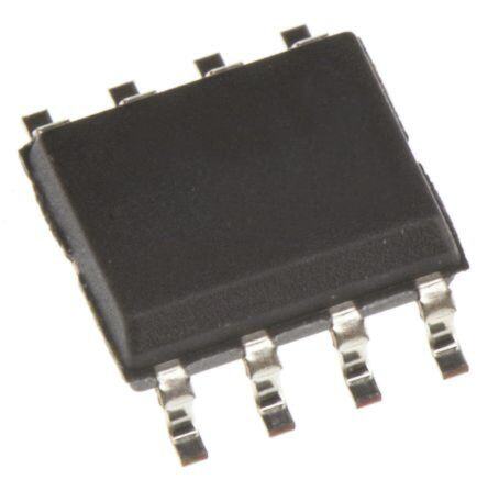
| 供应商器件封装 | 8-SOIC |
| 准确性 | 5 C |
| 包装 | 管件 |
| 商标 | Analog Devices |
| 增益 | + 1 uA / K |
| 安装风格 | SMD/SMT |
| 封装 | Tube |
| 封装/外壳 | 8-SOIC(0.154",3.90mm 宽) |
| 封装/箱体 | SOIC-8 |
| 工厂包装数量 | 98 |
| 感应温度 | -55°C ~ 150°C |
| 数字输出-总线接口 | 2-Wire, I2C, SMBus |
| 最大工作温度 | + 150 C |
| 最小工作温度 | - 55 C |
| 标准包装 | 98 |
| 电压-电源 | 4 V ~ 30 V |
| 电源电压-最大 | 30 V |
| 电源电压-最小 | 4 V |
| 精度 | ±5°C |
| 系列 | AD590 |
| 设备功能 | Temperature Transducer |
| 输出类型 | 电流 |


- 商务部:美国ITC正式对集成电路等产品启动337调查
- 曝三星4nm工艺存在良率问题 高通将骁龙8 Gen1或转产台积电
- 太阳诱电将投资9.5亿元在常州建新厂生产MLCC 预计2023年完工
- 英特尔发布欧洲新工厂建设计划 深化IDM 2.0 战略
- 台积电先进制程称霸业界 有大客户加持明年业绩稳了
- 达到5530亿美元!SIA预计今年全球半导体销售额将创下新高
- 英特尔拟将自动驾驶子公司Mobileye上市 估值或超500亿美元
- 三星加码芯片和SET,合并消费电子和移动部门,撤换高东真等 CEO
- 三星电子宣布重大人事变动 还合并消费电子和移动部门
- 海关总署:前11个月进口集成电路产品价值2.52万亿元 增长14.8%


PDF Datasheet 数据手册内容提取
2-Terminal IC Temperature Transducer Data Sheet AD590 FEATURES PIN CONFIGURATIONS Linear current output: 1 μA/K Wide temperature range: −55°C to +150°C V+ 1 4 NC Probe-compatible ceramic sensor package AD590 2-terminal device: voltage in/current out TOP VIEW (Not to Scale) Laser trimmed to ±0.5°C calibration accuracy (AD590M) PIN 5 (EXPOSEDPAD) Excellent linearity: ±0.3°C over full range (AD590M) V– 2 3 NC Wide power supply range: 4 V to 30 V Sensor isolation from case NOTES 1. NC = NO CONNECT. THE NC PIN IS NOT A v8a-illeaabdle S iOn I2C-,l eaandd FdLieA TfoPrAmC K, 4-lead LFCSP, 3-pin TO-52, + – 00533-024 2.TEBOXOP NEODNSESEDUDRTPEOA CTDOH (REE RPDE)I ECS THIN OOTUPELERDRN ABATELIL OLYEN.F, TT HFELOATING. 00533-104 GENERAL DESCRIPTION Figure 1. 2-Lead Figure 2. 4-Lead LFCSP FLATPACK The AD590 is a 2-terminal integrated circuit temperature trans- ducer that produces an output current proportional to absolute – temperature. For supply voltages between 4 V and 30 V, the device NC 1 8 NC acts as a high impedance, constant current regulator passing V+ 2 TOP VIEW 7 NC 1 μA/K. Laser trimming of the chip’s thin-film resistors is used + V– 3 (Not to Scale) 6 NC tToh cea AlibDr5at9e0 t shheo dueldvi bcee tuos e2d9 8in.2 aμnAy oteumtppuetr aattu 2r9e8-s.2e nKs i(n2g5 °C). 00533-025 NC N4C = NO CONNECT5 NC 00533-001 application below 150°C in which conventional electrical Figure 3. 3-Pin TO-52 Figure 4. 8-Lead SOIC temperature sensors are currently employed. The inherent low cost of a monolithic integrated circuit combined with the PRODUCT HIGHLIGHTS elimination of support circuitry makes the AD590 an attractive alternative for many temperature measurement situations. 1. The AD590 is a calibrated, 2-terminal temperature sensor requiring only a dc voltage supply (4 V to 30 V). Costly Linearization circuitry, precision voltage amplifiers, resistance transmitters, filters, lead wire compensation, and lineari- measuring circuitry, and cold junction compensation are not zation circuits are all unnecessary in applying the device. needed in applying the AD590. In addition to temperature measurement, applications include 2. State-of-the-art laser trimming at the wafer level in conjunction with extensive final testing ensures that temperature compensation or correction of discrete components, AD590 units are easily interchangeable. biasing proportional to absolute temperature, flow rate measure- ment, level detection of fluids and anemometry. The AD590 is 3. Superior interface rejection occurs because the output is a available in die form, making it suitable for hybrid circuits and current rather than a voltage. In addition, power fast temperature measurements in protected environments. requirements are low (1.5 mW @ 5 V @ 25°C). These features make the AD590 easy to apply as a remote sensor. The AD590 is particularly useful in remote sensing applications. The device is insensitive to voltage drops over long lines due to 4. The high output impedance (>10 MΩ) provides excellent its high impedance current output. Any well-insulated twisted rejection of supply voltage drift. For instance, changing the pair is sufficient for operation at hundreds of feet from the power supply from 5 V to 10 V results in only a 1 μA receiving circuitry. The output characteristics also make the maximum current change, or 1°C equivalent error. AD590 easy to multiplex: the current can be switched by a 5. The AD590 is electrically durable: it withstands a forward CMOS multiplexer, or the supply voltage can be switched by a voltage of up to 44 V and a reverse voltage of 20 V. logic gate output. Therefore, supply irregularities or pin reversal does not damage the device. Rev. G Document Feedback Information furnished by Analog Devices is believed to be accurate and reliable. However, no responsibility is assumed by Analog Devices for its use, nor for any infringements of patents or other One Technology Way, P.O. Box 9106, Norwood, MA 02062-9106, U.S.A. rights of third parties that may result from its use. Specifications subject to change without notice. No license is granted by implication or otherwise under any patent or patent rights of Analog Devices. Tel: 781.329.4700 ©2013 Analog Devices, Inc. All rights reserved. Trademarks and registered trademarks are the property of their respective owners. Technical Support www.analog.com
AD590 Data Sheet TABLE OF CONTENTS Features .....................................................................................1 Explanation of Temperature Sensor Specifications ................ 7 General Description ..................................................................1 Calibration Error ................................................................... 7 Pin Configurations ....................................................................1 Error vs. Temperature: Calibration Error Trimmed Out........ 7 Product Highlights ....................................................................1 Error vs. Temperature: No User Trims ................................... 7 Revision History ........................................................................2 Nonlinearity .......................................................................... 8 Specifications .............................................................................3 Voltage and Thermal Environment Effects ............................ 8 AD590J and AD590K Specifications ......................................3 General Applications ............................................................... 10 AD590L and AD590M Specifications ....................................4 Outline Dimensions ................................................................ 13 Absolute Maximum Ratings ......................................................5 Ordering Guide ................................................................... 15 ESD Caution ..........................................................................5 Product Description ..................................................................6 REVISION HISTORY 1/13—Rev. F to Rev. G Deleted Figure 22; Renumbered Sequentially .......................... 11 Changes to Endnote 2, Table 1 ...................................................3 Changes to Figure 21 and Figure 22 ........................................ 11 Changes to Ordering Guide .....................................................15 Deleted Figure 24 .................................................................... 12 Changes to Figure 24 ............................................................... 12 11/12—Rev. E to Rev. F Updated Outline Dimensions Section ..................................... 14 Added 4-Lead LFCSP_WD ......................................... Universal Changes to Ordering Guide..................................................... 14 Changes to Features Section, General Description Section, and Product Highlights Section........................................................1 9/09—Rev. D to Rev. E Added Figure 2; Renumbered Sequentially................................1 Changes to Product Description Section ................................... 6 Added Note 2, Table 1; Renumbered Sequentially .....................3 Updated Outline Dimensions .................................................. 13 Changes to (Unbolded) For 8-Lead SOIC Package, AD590J and Changes to Ordering Guide..................................................... 14 AD590K Parameter, Table 1.......................................................3 1/06—Rev. C to Rev. D Changes to Note 1, Table 3.........................................................5 Updated Format ...........................................................Universal Changes to Product Description Section ...................................6 Changes to Figure 4 Equation.................................................... 4 Change to Figure 6.....................................................................6 9/03—Rev. B to Rev. C Changes to Explanation of Temperature Sensor Specifications Added SOIC-8 Package ................................................Universal Section .......................................................................................7 Change to Figure 1 .................................................................... 1 Moved Nonlinearity Section ......................................................8 Updated Outline Dimensions .................................................. 13 Change to Figure 13...................................................................8 Added Ordering Guide............................................................ 14 Changes to General Applications Section ................................10 Changes to Figure 17 and Figure 19.........................................10 Rev. G | Page 2 of 16
Data Sheet AD590 SPECIFICATIONS AD590J AND AD590K SPECIFICATIONS 25°C and V = 5 V, unless otherwise noted.1 S Table 1. AD590J2 AD590K Parameter Min Typ Max Min Typ Max Unit POWER SUPPLY Operating Voltage Range 4 30 4 30 V OUTPUT Nominal Current Output @ 25°C (298.2 K) 298.2 298.2 µA Nominal Temperature Coefficient 1 1 µA/K Calibration Error @ 25°C ±5.0 ±2.5 °C Absolute Error (Over Rated Performance Temperature Range) Without External Calibration Adjustment ±10 ±5.5 °C With 25°C Calibration Error Set to Zero ±3.0 ±2.0 °C Nonlinearity For TO-52 and FLATPACK Packages ±1.5 ±0.8 °C For 8-Lead SOIC Package ±1.5 ±1.0 °C For 4-Lead LFCSP Package ±1.5 °C Repeatability3 ±0.1 ±0.1 °C Long-Term Drift4 ±0.1 ±0.1 °C Current Noise 40 40 pA/√Hz Power Supply Rejection 4 V ≤ V ≤ 5 V 0.5 0.5 µA/V S 5 V ≤ V ≤ 15 V 0.2 0.2 µV/V S 15 V ≤ V ≤ 30 V 0.1 0.1 µA/V S Case Isolation to Either Lead 1010 1010 Ω Effective Shunt Capacitance 100 100 pF Electrical Turn-On Time 20 20 µs Reverse Bias Leakage Current (Reverse Voltage = 10 V)5 10 10 pA 1 Specifications shown in boldface are tested on all production units at final electrical test. Results from those tests are used to calculate outgoing quality levels. All minimum and maximum specifications are guaranteed, although only those shown in boldface are tested on all production units. 2 The LFCSP package has a reduced operating temperature range of −40°C to +125°C. 3 Maximum deviation between +25°C readings after temperature cycling between −55°C and +150°C; guaranteed, not tested. 4 Conditions: constant 5 V, constant 125°C; guaranteed, not tested. 5 Leakage current doubles every 10°C. Rev. G | Page 3 of 16
AD590 Data Sheet AD590L AND AD590M SPECIFICATIONS 25°C and V = 5 V, unless otherwise noted.1 S Table 2. AD590L AD590M Parameter Min Typ Max Min Typ Max Unit POWER SUPPLY Operating Voltage Range 4 30 4 30 V OUTPUT Nominal Current Output @ 25°C (298.2 K) 298.2 298.2 μA Nominal Temperature Coefficient 1 1 μA/K Calibration Error @ 25°C ±1.0 ±0.5 °C Absolute Error (Over Rated Performance Temperature Range) °C Without External Calibration Adjustment ±3.0 ±1.7 °C With ± 25°C Calibration Error Set to Zero ±1.6 ±1.0 °C Nonlinearity ±0.4 ±0.3 °C Repeatability2 ±0.1 ±0.1 °C Long-Term Drift3 ±0.1 ±0.1 °C Current Noise 40 40 pA/√Hz Power Supply Rejection 4 V ≤ V ≤ 5 V 0.5 0.5 μA/V S 5 V ≤ V ≤ 15 V 0.2 0.2 μA/V S 15 V ≤ V ≤ 30 V 0.1 0.1 μA/V S Case Isolation to Either Lead 1010 1010 Ω Effective Shunt Capacitance 100 100 pF Electrical Turn-On Time 20 20 μs Reverse Bias Leakage Current (Reverse Voltage = 10 V)4 10 10 pA 1 Specifications shown in boldface are tested on all production units at final electrical test. Results from those tests are used to calculate outgoing quality levels. All minimum and maximum specifications are guaranteed, although only those shown in boldface are tested on all production units. 2 Maximum deviation between +25°C readings after temperature cycling between −55°C and +150°C; guaranteed, not tested. 3 Conditions: constant 5 V, constant 125°C; guaranteed, not tested. 4 Leakage current doubles every 10°C. °K +223° +273° +298° +323° +373° +423° °C –50° 0° +25° +50° +100° +150° °F –100° 0° +32° +70+°100° +20+02°12° +300° 00533-002 C5F32K C273.15 9 9 F C32 R F459.7 5 Figure 5. Temperature Scale Conversion Equations Rev. G | Page 4 of 16
Data Sheet AD590 ABSOLUTE MAXIMUM RATINGS Table 3. Stresses above those listed under Absolute Maximum Ratings Parameter Rating may cause permanent damage to the device. This is a stress Forward Voltage ( E+ or E−) 44 V rating only and functional operation of the device at these or Reverse Voltage (E+ to E−) −20 V any other conditions above those indicated in the operational Breakdown Voltage (Case E+ or E−) ±200 V section of this specification is not implied. Exposure to absolute Rated Performance Temperature Range1 −55°C to +150°C maximum rating conditions for extended periods may affect Storage Temperature Range1 −65°C to +155°C device reliability. Lead Temperature (Soldering, 10 sec) 300°C 1 The AD590 was used at −100°C and +200°C for short periods of ESD CAUTION measurement with no physical damage to the device. However, the absolute errors specified apply to only the rated performance temperature range. Applicable to 2-lead FLATPACK and 3-pin TO-52 packages only. Rev. G | Page 5 of 16
AD590 Data Sheet PRODUCT DESCRIPTION The AD590 is a 2-terminal temperature-to-voltage transducer. It Figure 8 shows the typical V–I characteristic of the circuit at is available in a variety of accuracy grades and packages. When 25°C and the temperature extremes. using the AD590 in die form, the chip substrate must be kept + electrically isolated (floating) for correct circuit operation. R1 R2 1725µM 260Ω 1040Ω Q2 Q5 Q3 Q1 Q4 C1 Q6 26pF V– 1090µM Q7 Q12 Q8 R4 V+ 00533-003 SUBSTRCAHTIEP R5k3Ω 11kΩ Figure 6. Metallization Diagram Q9 Q10 Q11 Ttrhane sAisDto5r9s 0f ruosmes wa hfuicnhd iatm ise mntaadl ep rtoo preeratlyiz oe fi ttsh tee smilpiceornat ure 8 R8260Ω 14R65Ω 1 1 00533-004 proportional characteristic: if two identical transistors are – operated at a constant ratio of collector current densities, r, Figure 7. Schematic Diagram then the difference in their base-emitter voltage is (kT/q)(In r). Because both k (Boltzman’s constant) and q (the charge of an electron) are constant, the resulting voltage is directly pro- portional to absolute temperature (PTAT). (For a more detailed +150°C description, see M.P. Timko, “A Two-Terminal IC Temperature 423 Transducer,” IEEE J. Solid State Circuits, Vol. SC-11, p. 784-788, Dec. 1976. Understanding the Specifications–AD590.) µA) 298 +25°C In the AD590, this PTAT voltage is converted to a PTAT current (UT O –55°C by low temperature coefficient thin-film resistors. The total I 218 current of the device is then forced to be a multiple of this PTAT current. Figure 7 is the schematic diagram of the AD590. In this figure, Q8 and Q11 are the transistors that produce the PTAT voltage. R5 and R6 convert the voltage to current. Q10, 00533-005 whose collector current tracks the collector currents in Q9 and 0 1 2 3 4 5 6 30 Q11, supplies all the bias and substrate leakage current for the SUPPLY VOLTAGE (V) Figure 8. V–I Plot rest of the circuit, forcing the total current to be PTAT. R5 and R6 are laser-trimmed on the wafer to calibrate the device at 25°C. Rev. G | Page 6 of 16
Data Sheet AD590 EXPLANATION OF TEMPERATURE SENSOR temperature range. In most applications, there is a current-to- SPECIFICATIONS voltage conversion resistor (or, as with a current input ADC, a reference) that can be trimmed for scale factor adjustment. The way in which the AD590 is specified makes it easy to apply it in a wide variety of applications. It is important to understand 5V + + the meaning of the various specifications and the effects of the AD590 – supply voltage and thermal environment on accuracy. + R The AD590 is a PTAT current regulator. (Note that T (°C) = 100Ω Tno ( Klo)w −e r2 t7e3m.2p. eZreartou roen.) tThhe aKt eislv, itnh es coauletp ius ta cbusorrluentet zise reoq;u tahle troe ais – 950Ω VT = 1m–V/K 00533-007 scale factor times the temperature of the sensor in degrees Figure 10. One Temperature Trim Kelvin. This scale factor is trimmed to 1 μA/K at the factory, by ERROR VS. TEMPERATURE: CALIBRATION ERROR adjusting the indicated temperature (that is, the output current) TRIMMED OUT to agree with the actual temperature. This is done with 5 V across the device at a temperature within a few degrees of 25°C Each AD590 is tested for error over the temperature range with (298.2 K). The device is then packaged and tested for accuracy the calibration error trimmed out. This specification could also over temperature. be called the variance from PTAT, because it is the maximum difference between the actual current over temperature and a CALIBRATION ERROR PTAT multiplication of the actual current at 25°C. This error At final factory test, the difference between the indicated consists of a slope error and some curvature, mostly at the temperature and the actual temperature is called the calibration temperature extremes. Figure 11 shows a typical AD590K error. Since this is a scale factory error, its contribution to the temperature curve before and after calibration error trimming. total error of the device is PTAT. For example, the effect of the 1°C specified maximum error of the AD590L varies from 0.73°C at −55°C to 1.42°C at 150°C. Figure 9 shows how an exaggerated 2 calibration error would vary from the ideal over temperature. BEFORE C) CALIBRATION R (° TRIM RO CALIBRATION R ERROR ACTUAL E TRANSFER E FUNCTION UT 0 L O S B A AFTER A) IACTUAL CALIBRATION I (µOUT 298.2 CERARLIOBRRATION TFRUIANDNCESTAFILOENR –2 TRIM 00533-008 –55 150 TEMPERATURE (°C) Figure 11. Effect to Scale Factor Trim on Accuracy 00533-006 ERROR VS. TEMPERATURE: NO USER TRIMS 298.2 Using the AD590 by simply measuring the current, the total TEMPERATURE (°K) Figure 9. Calibration Error vs. Temperature error is the variance from PTAT, described above, plus the effect of the calibration error over temperature. For example, the The calibration error is a primary contributor to the maximum AD590L maximum total error varies from 2.33°C at −55°C to total error in all AD590 grades. However, because it is a scale 3.02°C at 150°C. For simplicity, only the large figure is shown factor error, it is particularly easy to trim. Figure 10 shows the on the specification page. most elementary way of accomplishing this. To trim this circuit, the temperature of the AD590 is measured by a reference temperature sensor and R is trimmed so that V T = 1 mV/K at that temperature. Note that when this error is trimmed out at one temperature, its effect is zero over the entire Rev. G | Page 7 of 16
AD590 Data Sheet NONLINEARITY Nonlinearity as it applies to the AD590 is the maximum 2 deviation of current over temperature from a best-fit straight line. The nonlinearity of the AD590 over the −55°C to +150°C C) range is superior to all conventional electrical temperature E (° R sensors such as thermocouples, RTDs, and thermistors. Figure 12 TU A R shows the nonlinearity of the typical AD590K from Figure 11. PE 0 M E T 1.6 R (°C) 0.8 –2 00533-011 O –55 0 100 150 R R 0.8°C MAX TEMPERATURE (°C) E E Figure 14. Typical 2-Trim Accuracy T 0 U OL 0.8°C 0.8°C VOLTAGE AND THERMAL ENVIRONMENT EFFECTS BS MAX MAX A The power supply rejection specifications show the maximum –0.8 expected change in output current vs. input voltage changes. –1.6 00533-009 Tunhree ignusleantesdit isvuitpyp olife sth. Iet oaulstop umt etoan ins pthuatt v houltnadgere adlslo owf so thhme su osef of –55 150 TEMPERATURE (°C) resistance (such as a CMOS multiplexer) can be tolerated in Figure 12. Nonlinearity series with the device. Figure 13 shows a circuit in which the nonlinearity is the major It is important to note that using a supply voltage other than 5 V contributor to error over temperature. The circuit is trimmed does not change the PTAT nature of the AD590. In other words, by adjusting R1 for a 0 V output with the AD590 at 0°C. R2 is this change is equivalent to a calibration error and can be then adjusted for 10 V output with the sensor at 100°C. Other removed by the scale factor trim (see Figure 11). pairs of temperatures can be used with this procedure as long as The AD590 specifications are guaranteed for use in a low they are measured accurately by a reference sensor. Note that thermal resistance environment with 5 V across the sensor. for 15 V output (150°C), the V+ of the op amp must be greater Large changes in the thermal resistance of the sensor’s environment than 17 V. Also, note that V− should be at least −4 V; if V− is change the amount of self-heating and result in changes in the ground, there is no voltage applied across the device. output, which are predictable but not necessarily desirable. 15V The thermal environment in which the AD590 is used R1 R2 35.7kΩ 2kΩ 97.6kΩ 5kΩ determines two important characteristics: the effect of self- AD581 heating and the response of the sensor with time. Figure 15 is a 30pF model of the AD590 that demonstrates these characteristics. 27kΩ TJ θJC TC θCA OP177 100mV/°C VT = 100mV/°C + V–AD590 00533-010 P CCH CC –TA 00533-012 Figure 13. 2-Temperature Trim Figure 15. Thermal Circuit Model Rev. G | Page 8 of 16
Data Sheet AD590 As an example, for the TO-52 package, θ is the thermal The time response of the AD590 to a step change in JC resistance between the chip and the case, about 26°C/W. θ is temperature is determined by the thermal resistances and the CA the thermal resistance between the case and the surroundings thermal capacities of the chip, C , and the case, C . C is CH C CH and is determined by the characteristics of the thermal about 0.04 Ws/°C for the AD590. C varies with the measured C connection. Power source P represents the power dissipated medium, because it includes anything that is in direct thermal on the chip. The rise of the junction temperature, T, above the contact with the case. The single time constant exponential J ambient temperature, T , is curve of Figure 16 is usually sufficient to describe the time A response, T (t). Table 4 shows the effective time constant, τ, for T − T = P(θ + θ ) (1) J A JC CA several media. Table 4 gives the sum of θ and θ for several common JC CA thermal media for both the H and F packages. The heat sink used was a common clip-on. Using Equation 1, the temperature TFINAL rise of an AD590 H package in a stirred bath at 25°C, when E driven with a 5 V supply, is 0.06°C. However, for the same UR T conditions in still air, the temperature rise is 0.72°C. For a given RA E supply voltage, the temperature rise varies with the current and MP E is PTAT. Therefore, if an application circuit is trimmed with the D T T(t) = TINITIAL + (TFINAL – TINITIAL)× (1 – e–t/) sensor in the same thermal environment in which it is used, the SE N scale factor trim compensates for this effect over the entire SE temperature range. Table 4. Thermal Resistance θJC + θCA TINITIAL 4 00533-013 (°C/Watt) τ (sec)1 TIME Medium H F H F Figure 16. Time Response Curve Aluminum Block 30 10 0.6 0.1 Stirred Oil2 42 60 1.4 0.6 Moving Air3 With Heat Sink 45 – 5.0 – Without Heat Sink 115 190 13.5 10.0 Still Air With Heat Sink 191 – 108 – Without Heat Sink 480 650 60 30 1 τ is dependent upon velocity of oil; average of several velocities listed above. 2 Air velocity @ 9 ft/sec. 3 The time constant is defined as the time required to reach 63.2% of an instantaneous temperature change. Rev. G | Page 9 of 16
AD590 Data Sheet GENERAL APPLICATIONS Figure 17 shows a typical use of the AD590 in a remote V+ temperature sensing application. The AD590 is used as a + R3 thermometer circuit that measures temperature from −55°C to AD590L 10kΩ #2 – +150°C, with an output voltage of 1 mV/°K. Because the AD590 measures absolute temperature (its nominal output is – OP177 1 mA/K), the output must be offset by 273.2 mA to read out in + R1 degrees Celsius. –AD#5190L R2 5MΩ R4 + (T1 – T2)×(10mV/°C) 50kΩ 10kΩ AD590 IT + V– 00533-016 7V Figure 19. Differential Measurements – Figure 20 is an example of a cold junction compensation circuit for a Type J thermocouple using the AD590 to monitor the IT IT reference junction temperature. This circuit replaces an ice-bath as the thermocouple reference for ambient temperatures between 15°C and 35°C. The circuit is calibrated by adjusting R 1k T 0.1% LOW for a proper meter reading with the measuring junction at a TCR RESISTOR 1mV/k known reference temperature and the circuit near 25°C. Using 00533-014 caoccmupraocnye inst sw witihthin t h±e0 T.5C°Cs a fso srp ceicricfiueidt tinem Fpigeurraet u2r0e, sc obmetpweenesnat i1o5n°C Figure 17. Variable Scale Display and 35°C. Other thermocouple types can be accommodated with Connecting several AD590 units in series, as shown in Figure 18, different resistor values. Note that the TCs of the voltage allows the minimum of all the sensed temperatures to be reference and the resistors are the primary contributors to error. indicated. In contrast, using the sensors in parallel yields the 7.5V average of the sensed temperatures. IRON REFERENCE 15V JUNCTION + + CONSTANTAN AD590 AD590 – 5V – + + AD590 + + + – – AD590 + AD580 52.3Ω CU + – – – MEASURING AD590 – VOUT + – JUNCTION – 8.66kΩ + + (01.01k%Ω)Figure 18V.T S– MerINies and3 (3P03.a1.3r%aΩ)llel ConneVcTt–AioVnG 00533-015 1kRΩT RMESEITSETRORSARE 1%, 50ppm/°C 00533-017 The circuit in Figure 19 demonstrates one method by which Figure 20. Cold Junction Compensation Circuit for Type J Thermocouple differential temperature measurements can be made. R1 and R2 can be used to trim the output of the op amp to indicate a desired temperature difference. For example, the inherent offset between the two devices can be trimmed in. If V+ and V− are radically different, then the difference in internal dissipation causes a differential internal temperature rise. This effect can be used to measure the ambient thermal resistance seen by the sensors in applications such as fluid-level detectors or anemometry. Rev. G | Page 10 of 16
Data Sheet AD590 Figure 21 is an example of a current transmitter designed to be V+ used with 40 V, 1 kΩ systems; it uses its full current range of 4 AD581 V+ OUT 10V to 20 mA for a narrow span of measured temperatures. In this HEATING example, the 1 µA/K output of the AD590 is amplified to V– RH AD590 + RB ELEMENTS 1 mA/°C and offset so that 4 mA is equivalent to 17°C and – 2 7 20 mA is equivalent to 33°C. R is trimmed for proper reading RSET – T AD790 at an intermediate reference temperature. With a suitable choice 1 of resistors, any temperature range within the operating limits RL 3 + 4 of the AD590 can be chosen. C1 10kΩ V+ GND 00533-019 Figure 22. Simple Temperature Control Circuit + AD581 4mA = 17°C 2102mmAA == 3235°°CC – VOUT The voltage compliance and the reverse blocking characteristic 35.7kΩ of the AD590 allow it to be powered directly from 5 V CMOS AD590+ 5kRΩT – 30pF lmoginici.m Tuhmis ipnetremrniatsl heaesayt mdisuslitpipalteixoinn. gI,n s wFiigtuchrein 2g3,, oarn pyu AlsDin5g9 f0o r – OP177 connected to a logic high passes a signal current through the + 5kΩ 500Ω current measuring circuitry, while those connected to a logic 12.7kΩ zero pass insignificant current. The outputs used to drive the 0.01µF 10kΩ 10Ω AD590s can be employed for other purposes, but the additional V– 00533-018 capacitance due to t5hVe AD590 should be taken into account. Figure 21. 4 to 20 mA Current Transmitter Figure 22 is an example of a variable temperature control circuit (thermostat) using the AD590. RH and RL are selected to set the + AD590 high and low limits for R . R could be a simple pot, a SET SET CMOS + – calibrated multiturn pot, or a switched resistive divider. Powering GATES the AD590 from the 10 V reference isolates the AD590 from + – supply variations while maintaining a reasonable voltage (~7 V) + – across it. Capacitor C1 is often needed to filter extraneous noise from remote sensors. R is determined by the β of the power – B transistor and the current requirements of the load. 1kΩ (0.1%) 00533-021 Figure 23. AD590 Driven from CMOS Logic Rev. G | Page 11 of 16
AD590 Data Sheet Figure 24 demonstrates a method of multiplexing the AD590 in temperature range of −55°C to +125°C. The high temperature the 2-trim mode (see Figure 13 and Figure 14). Additional restriction of 125°C is due to the output range of the op amps; AD590s and their associated resistors can be added to multiplex output to 150°C can be achieved by using a 20 V supply for the up to eight channels of ±0.5°C absolute accuracy over the op amp. 2kΩ 5kΩ +15V 35.7kΩ 97.6kΩ + 35.7kΩ2kΩ 5kΩ 97.6kΩ AD581 – VOUT V+ S1 OP177 10mV/°C S2 DECODER/ DRIVER 27kΩ–15V S8 AD7501 +15V TTL/DTLTO CMOS –15V INTERFACE + + EN AD590L AD590L BINARY – – CHANNEL SELECT –5VTO –15V 00533-023 Figure 24. 8-Channel Multiplexer Rev. G | Page 12 of 16
Data Sheet AD590 OUTLINE DIMENSIONS 0.030 (0.76) TYP 0.019 (0.48) POSITIVE LEAD INDICATOR 0.017 (0.43) 0.015 (0.38) 0.093 (2.36) 0.081 (2.06) 0.055 (1.40) 0.050 (1.27) 0.045 (1.14) 0.500 (12.69) 0.210 (5.34) MIN 0.200 (5.08) 0.190 (4.83) 0.240 (6.10) 0.230 (5.84) 0.220 (5.59) 0.0065 (0.17) 0.050 (1.27) 0.0050 (0.13) 0.041 (1.04) 0.0045 (0.12) 0.015 (0.38) TYP Figure 25. 2-Lead Ceramic Flat Package [FLATPACK] (F-2) Dimensions shown in inches and (millimeters) 0.500 (12.70) MIN 0.150 (3.81) 0.115 (2.92) 0.250 (6.35) MIN 0.050 (1.27)T.P. 0.050 (1.27) MAX 0.048 (1.22) 0 (5.84)9 (5.31) 5 (4.95)8 (4.52) (02..15040) 2 3 0.028 (0.71) 2320 1917 T.P. 0.046 (1.17) 0.0. 0.0. 0.019 (0.48) 0.050 1 0.036 (0.91) 0.016 (0.41) (1.27) T.P. 0.030 (0.76) MAX 0.021 (0.53) MAX 45°T.P. BASE & SEATING PLANE C(RINOEFNPEATRRREOENNLCLTEIHN EOGSN EDLSIYM)AEANNRDSEI AORRNOESU NANORDEET DAIN-PO IPFNRFCO HINPECRSHI;A METEQIL UFLIOIVMRAE LUTEESNRET DISNI M FDOEERNSSIGIONN.S 022306-A Figure 26. 3-Pin Metal Header Package [TO-52] (H-03-1) Dimensions shown in inches and (millimeters) Rev. G | Page 13 of 16
AD590 Data Sheet 5.00(0.1968) 4.80(0.1890) 8 5 4.00(0.1574) 6.20(0.2441) 3.80(0.1497) 1 4 5.80(0.2284) 1.27(0.0500) 0.50(0.0196) BSC 1.75(0.0688) 0.25(0.0099) 45° 0.25(0.0098) 1.35(0.0532) 8° 0.10(0.0040) 0° COPLANARITY 0.51(0.0201) 0.10 SEATING 0.31(0.0122) 0.25(0.0098) 10..2470((00..00510507)) PLANE 0.17(0.0067) COMPLIANTTOJEDECSTANDARDSMS-012-AA C(RINOEFNPEATRRREOENNLCLTEIHNEOGSNDELISYM)AEANNRDSEIAORRNOESUNANORDETEDAIN-POMPFRIFLOLMPIMIRLELIATIMTEEERTFSEO;RIRNECUQHSUEDIVIINMAELDENENSSTIIOGSNNFS.OR 012407-A Figure 27. 8-Lead Standard Small Outline Package [SOIC_N] Narrow Body (R-8) Dimensions shown in millimeters and (inches) 1.65 2.10 1.55 2.00 1.45 1.90 0.80 REF 3 4 0.20 MIN 3.10 EXPOSED 1.80 3.00 PAD 1.70 PIN 1 INDEX 2.90 0.50 1.60 AREA 0.40 0.30 2 1 PIN 1 TOP VIEW BOTTOM VIEW INDICATOR (R 0.15) 0.80 0.203 REF 0.05 MAX FTHOER EPXRPOOPSEERD C POANDN, ERCETFIEORN TOOF 0.75 0.00 MIN THE PIN CONFIGURATIONS 0.70 SECTION OF THIS DATA SHEET. SEATING 0.35 PLANE 0.30 C0.O08PLANARITY 0.25 COMPLIANTTOJEDEC STANDARDS MO-229 09-07-2010-B Figure 28. 4-Lead Lead Frame Chip Scale Package [LFCSP_WD] 2.00 mm × 3.00 mm Body, Very Very Thin, Dual Lead (CP-4-1) Dimensions shown in millimeters Rev. G | Page 14 of 16
Data Sheet AD590 ORDERING GUIDE Model1, 2 Temperature Range Package Description Package Option Branding AD590JF −55°C to +150°C 2-Lead FLATPACK F-2 AD590JH −55°C to +150°C 3-Pin TO-52 H-03-1 AD590JR −55°C to +150°C 8-Lead SOIC_N R-8 AD590JRZ −55°C to +150°C 8-Lead SOIC_N R-8 AD590KF −55°C to +150°C 2-Lead FLATPACK F-2 AD590KH −55°C to +150°C 3-Pin TO-52 H-03-1 AD590KR −55°C to +150°C 8-Lead SOIC_N R-8 AD590KR-REEL −55°C to +150°C 8-Lead SOIC_N R-8 AD590KRZ −55°C to +150°C 8-Lead SOIC_N R-8 AD590KRZ-RL −55°C to +150°C 8-Lead SOIC_N R-8 AD590LF −55°C to +150°C 2-Lead FLATPACK F-2 AD590LH −55°C to +150°C 3-Pin TO-52 H-03-1 AD590MF −55°C to +150°C 2-Lead FLATPACK F-2 AD590MH −55°C to +150°C 3-Pin TO-52 H-03-1 AD590JCHIPS −55°C to +150°C Bare Die H-03-1 AD590JCPZ-R5 −40°C to +125°C 4-Lead LFCSP_WD CP-4-1 7A AD590JCPZ-RL7 −40°C to +125°C 4-Lead LFCSP_WD CP-4-1 7A 1 Z = RoHS Compliant Part. 2 The AD590xF models and the AD590xH models are available in 883B. Rev. G | Page 15 of 16
AD590 Data Sheet NOTES ©2013 Analog Devices, Inc. All rights reserved. Trademarks and registered trademarks are the property of their respective owners. D00533-0-1/13(G) Rev. G | Page 16 of 16
Mouser Electronics Authorized Distributor Click to View Pricing, Inventory, Delivery & Lifecycle Information: A nalog Devices Inc.: AD590JF/883B AD590KH AD590KRZ AD590JCPZ-R5 AD590JH AD590LH AD590MF/883B AD590JH/883B AD590LH/883B 5962-8757103YA AD590KH/883B AD590KF AD590MH AD590MF AD590KF/883B 5962- 8757101XA AD590LF/883B AD590JR 5962-8757102YA 5962-8757103XA AD590JRZ 5962-8757102XA 5962- 8757104YA AD590KRZ-RL AD590JF AD590LF 5962-8757101YA AD590JCPZ-RL7 AD590KR AD590MH/883B