ICGOO在线商城 > 集成电路(IC) > 数据采集 - 模数转换器 > AD570JD
 Datasheet下载
- 型号: AD570JD
- 制造商: Analog
- 库位|库存: xxxx|xxxx
- 要求:
| 数量阶梯 | 香港交货 | 国内含税 |
| +xxxx | $xxxx | ¥xxxx |
查看当月历史价格
查看今年历史价格
AD570JD产品简介:
ICGOO电子元器件商城为您提供AD570JD由Analog设计生产,在icgoo商城现货销售,并且可以通过原厂、代理商等渠道进行代购。 AD570JD价格参考。AnalogAD570JD封装/规格:数据采集 - 模数转换器, 8 Bit Analog to Digital Converter 1 Input 1 SAR 18-CDIP。您可以下载AD570JD参考资料、Datasheet数据手册功能说明书,资料中有AD570JD 详细功能的应用电路图电压和使用方法及教程。
AD570JD 是由 Analog Devices Inc.(ADI)生产的一款数据采集模数转换器(ADC)。该型号属于高性能、低功耗的 12 位逐次逼近寄存器(SAR)型 ADC,广泛应用于需要高精度和快速采样的场景。以下是 AD570JD 的主要应用场景:

 1. 工业自动化与控制
   - 在工业自动化中,AD570JD 可用于实时监测和控制各种参数,例如温度、压力、流量和液位等。
   - 它能够将传感器输出的模拟信号(如电压或电流)转换为数字信号,以便微控制器或处理器进行处理和分析。
   - 常见应用包括可编程逻辑控制器(PLC)、分布式控制系统(DCS)和智能仪表。

 2. 医疗设备
   - 医疗领域中,AD570JD 可用于患者监护设备,如心电图(ECG)、血压监测仪和血糖仪。
   - 其高精度特性确保了对生物电信号的准确采集,从而提高了诊断和治疗的可靠性。
   - 此外,它还适用于超声波设备中的信号数字化处理。

 3. 通信系统
   - 在通信领域,AD570JD 可用于射频(RF)信号的采集和分析。
   - 它支持高速采样率,能够满足无线通信系统中对信号带宽的需求。
   - 应用实例包括基站接收器、软件定义无线电(SDR)和卫星通信设备。

 4. 汽车电子
   - 汽车行业中,AD570JD 可用于发动机控制单元(ECU)、胎压监测系统(TPMS)和车载娱乐系统。
   - 它能够精确测量发动机温度、油压和其他关键参数,帮助优化车辆性能并提高安全性。

 5. 消费电子
   - 在消费电子产品中,AD570JD 可用于音频设备、家用电器和智能家居系统。
   - 例如,在音频设备中,它可用于将麦克风输入的模拟信号转换为数字信号,以实现高质量的声音记录和播放。

 6. 测试与测量
   - AD570JD 广泛应用于示波器、信号发生器和功率计等测试设备中。
   - 它的高分辨率和低噪声特性使其成为精密测量的理想选择,能够准确捕捉复杂信号的变化。

 总结
AD570JD 凭借其高精度、低功耗和灵活的接口设计,适合多种需要模拟信号数字化的应用场景。无论是工业控制、医疗设备还是通信系统,它都能提供可靠的性能和稳定的输出,满足不同领域的技术需求。
| 参数 | 数值 |
| 产品目录 | 集成电路 (IC)半导体 |
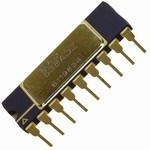
| 描述 | IC ADC 8BIT MONO W/CLK 18-CDIP模数转换器 - ADC IC MONO 8-BIT |
| 产品分类 | |
| 品牌 | Analog Devices |
| 产品手册 | |
| 产品图片 |
|
| rohs | 否不符合限制有害物质指令(RoHS)规范要求 |
| 产品系列 | 数据转换器IC,模数转换器 - ADC,Analog Devices AD570JD- |
| 数据手册 | |
| 产品型号 | AD570JD |
| PCN设计/规格 | |
| 产品种类 | 模数转换器 - ADC |
| 位数 | 8 |
| 供应商器件封装 | 18-CDIP |
| 分辨率 | 8 bit |
| 包装 | 管件 |
| 商标 | Analog Devices |
| 安装类型 | 通孔 |
| 安装风格 | Through Hole |
| 封装 | Tube |
| 封装/外壳 | 18-CDIP(0.300",7.62mm) |
| 封装/箱体 | CDIP-18 SB |
| 工作温度 | 0°C ~ 70°C |
| 工作电源电压 | 5 V, 15 V |
| 工厂包装数量 | 20 |
| 接口类型 | Parallel |
| 数据接口 | 并联 |
| 最大功率耗散 | 275 mW |
| 最大工作温度 | + 125 C |
| 最小工作温度 | - 55 C |
| 标准包装 | 1 |
| 特性 | - |
| 电压参考 | Internal |
| 电压源 | 双 ± |
| 系列 | AD570 |
| 结构 | SAR |
| 转换器数 | 1 |
| 转换器数量 | 1 |
| 输入数和类型 | 1 个单端,单极1 个单端,双极 |
| 输入类型 | Single-Ended |
| 通道数量 | 1 Channel |
| 采样率(每秒) | 40k |


- 商务部:美国ITC正式对集成电路等产品启动337调查
- 曝三星4nm工艺存在良率问题 高通将骁龙8 Gen1或转产台积电
- 太阳诱电将投资9.5亿元在常州建新厂生产MLCC 预计2023年完工
- 英特尔发布欧洲新工厂建设计划 深化IDM 2.0 战略
- 台积电先进制程称霸业界 有大客户加持明年业绩稳了
- 达到5530亿美元!SIA预计今年全球半导体销售额将创下新高
- 英特尔拟将自动驾驶子公司Mobileye上市 估值或超500亿美元
- 三星加码芯片和SET,合并消费电子和移动部门,撤换高东真等 CEO
- 三星电子宣布重大人事变动 还合并消费电子和移动部门
- 海关总署:前11个月进口集成电路产品价值2.52万亿元 增长14.8%


PDF Datasheet 数据手册内容提取
B 781/329.4700 781/461.3113
AD570–SPECIFICATIONS (TA = +25(cid:56)C, V+ = +5 V, V– = –12 V or –15 V, all voltages measured with respect to digital common, unless otherwise noted) AD570J AD570S Model Min Typ Max Min Typ Max Units RESOLUTION1 8 8 Bits RELATIVE ACCURACY LSB T to T (cid:54)1/2 (cid:54)1/2 LSB MIN MAX FULL-SCALE CALIBRATION – 2 – 2 LSB UNIPOLAR OFFSET (cid:54)1/2 (cid:54)1/2 LSB BIPOLAR OFFSET (cid:54)1/2 (cid:54)1/2 LSB DIFFERENTIAL NONLINEAIRTY T to T 8 8 Bits MIN MAX TEMPERATURE RANGE 0 +70 –55 +125 (cid:176) C TEMPERATURE COEFFICIENTS Unipolar Offset (cid:54)1 (cid:54)1 LSB Bipolar Offset (cid:54)1 (cid:54)1 LSB Full-Scale Calibration (cid:54)2 (cid:54)2 LSB POWER SUPPLY REJECTION TTL Positive Supply +4.5 V £ V + £ +5.5 V (cid:54)2 (cid:54)2 LSB Negative Supply –16.0 V £ V – £ –13.5 V (cid:54)2 (cid:54)2 LSB ANALOG INPUT IMPEDANCE 3.0 5.0 7.0 3.0 5.0 7.0 kW ANALOG INPUT RANGES Unipolar 0 +10 0 +10 V Bipolar –5 +5 –5 +5 V OUTPUT CODING Unipolar Positive True Binary Positive True Binary Bipolar Positive True Offset Binary Positive True Offset Binary LOGIC OUTPUT Output Sink Current (V = 0.4 V max, T to T ) 3.2 3.2 mA OUT MIN MAX Output Source Current (V = 2.4 V max, T to T ) 0.5 0.5 mA OUT MIN MAX Output Leakage (cid:54)40 (cid:54)40 m A LOGIC INPUTS Input Current (cid:54)100 (cid:54)100 m A Logic “1” 2.0 2.0 V Logic “0” 0.8 0.8 V CONVERSION TIME 15 25 40 15 25 40 m s POWER SUPPLY V+ +4.5 +5.0 +7.0 +4.5 +5.0 +7.0 V V– –12.0 –15 –16.5 –12.0 –15 –16.5 V OPERATING CURRENT V+ 7 15 7 15 mA V– 9 15 9 15 mA PACKAGE OPTION2 Ceramic DIP (D-18) AD570JD AD570SD NOTES 1The AD570 is a selected version of the AD571 10-bit A-to-D converter. Only TTL logic inputs should be connected to Pins 1 and 18 (or no connection made) or damage may result. 2For details on grade package offerings for SD-grade in accorance with MIL-STD-883, refer to Analog Devices’ Military Products databook or current /883 data sheet. Specifications subject to change without notice. Specifications shown in boldface are tested on all production units at final electrical test. Results from those tests are used to calculate outgoing quality levels. All min and max specifications are guaranteed, although only those shown in boldface are tested on all production units. –2– REV. B
AD570 ABSOLUTE MAXIMUM RATINGS signal, an input current will be generated which exactly matches V+ to Digital Common . . . . . . . . . . . . . . . . . . . . . 0 V to +7 V the DAC output with all bits on. (The input resistor is trimmed V– to Digital Common . . . . . . . . . . . . . . . . . . 0 V to –16.5 V slightly low to facilitate user trimming, as discussed on the next Analog Common to Digital Common . . . . . . . . . . . . . . . – 1 V page.) Analog Input to Analog Common . . . . . . . . . . . . . . . . . – 15 V POWER SUPPLY SELECTION Control Inputs . . . . . . . . . . . . . . . . . . . . . . . . . . . . . .0 V to V+ The AD570 is designed and specified for optimum performance Digital Outputs (Blank Mode) . . . . . . . . . . . . . . . . . .0 V to V+ using a +5 V and –15 V supply. The supply current drawn by Power Dissipation. . . . . . . . . . . . . . . . . . . . . . . . . . . . .800 mW the device is a function of the operating mode (BLANK or CONVERT), as given on the specification page. The supply CIRCUIT DESCRIPTION currents change only moderately over temperature as shown in The AD570 is a complete 8-bit A/D converter which requires Figure 2, and do not change significantly with changes in V– no external components to provide the complete successive- from –10.8 volts to –16 volts. approximation analog-to-digital conversion function. A block diagram of the AD570 is shown on last page. Upon receipt of the CONVERT command, the internal 8-bit current output DAC is sequenced by the I2L successive-approximation register (SAR) from its most-significant bit (MSB) to least-significant bit (LSB) to provide an output current which accurately bal- ances the input signal current through the 5 kW input resistor. The comparator determines whether the addition of each suc- cessively-weighted bit current causes the DAC current sum to be greater or less than the input current; if the sum is less the bit is left on, if more, the bit is turned off. After testing all the bits, the SAR contains a 8-bit binary code which accurately repre- sents the input signal to within – 1/2 LSB (0.20%). Upon completion of the sequence, the DATA READY signal goes low, and the bit output lines become active high or low depending on the code in the SAR. When the BLANK and CONVERT line is brought high, the output buffers again go “open”, and the SAR is prepared for another conversion cycle. The temperature compensated buried Zener reference provides Figure 2.AD570 Power Supply Current vs. Temperature the primary voltage reference to the DAC and guarantees excel- lent stability with both time and temperature. The bipolar offset CONNECTING THE AD570 FOR STANDARD input controls a switch which allows the positive bipolar offset OPERATION current (exactly equal to the value of the MSB less 1/2 LSB) The AD570 contains all the active components required to per- form a complete A/D conversion. Thus, for most situations, all that is necessary is to connect the power supply (+5 V and –15 V), BIT 2 BIT 3 BIT 4 BIT 5 BIT 6 BIT 7 BIT 8 LSB the analog input, and the conversion start signal. But, there are some features and special connections which should be consid- ered for achieving optimum performance. The functional pinout BIT 1 MSB is shown in Figure 3. V+ BLANK & CONV DATA READY 0.120 DIGITAL COMMON BIPOLAR V– OFFSET CONTROL ANALOG COMMON ANALOG IN 0.151 THE AD570 IS ALSO AVAILABLE IN A LASER-TRIMMED PASSIVATED CHIP FORM. CONSULT CHIP CATALOG FOR APPLICATION PARTICULARS. FIGURE 3 SHOWS THE CHIP METALLIZATION LAYOUT AND BONDING PADS. Figure 1.Chip Bonding Diagram to be injected into the summing (+) node of the comparator to offset the DAC output. Thus the nominal 0 V to +10 V unipo- Figure 3.AD570 Pin Connections lar input range becomes a –5 V to +5 V range. The 5 kW thin- film input resistor is trimmed so that with a full-scale input REV. B –3–
AD570 FULL-SCALE CALIBRATION The 5 kW thin-film input resistor is laser trimmed to produce a current which matches the full-scale current of the internal DAC—plus about 0.3%—when a full-scale analog input voltage of 9.961 volts (10 volts—1 LSB) is applied at the input. The in- put resistor is trimmed in this way so that if a fine trimming potentiometer is inserted in series with the input signal, the in- put current at the full-scale input voltage can be trimmed down to match the DAC full-scale current as precisely as desired. However, for many applications the nominal 9.961 volt full scale can be achieved to sufficient accuracy by simply inserting a 15 W resistor in series with the analog input to Pin 13. Typical full-scale calibration error will then be about – 2 LSB or – 0.8%. If a more precise calibration is desired, a 200 W trimmer should be used instead. Set the analog input at 9.961 volts, and set the trimmer so that the output code is just at the transition between 11111110 and 11111111. Each LSB will then have a weight of Figure 5.Bipolar Offset Controlled by Logic Gate 39.06 mV. If a nominal full scale of 10.24 volts is desired Gate Output = 1: Unipolar 0 V–10 V Input Range (which makes the LSB have a value of exactly 40.00 mV), a Gate Output = 0: Bipolar – 5 V Input Range 50 W resistor in series with a 200 W trimmer (or a 500 W trim- mer with good resolution) should be used. Of course, larger full- COMMON-MODE RANGE scale ranges can be arranged by using a larger input resistor, but The AD570 provides separate analog and digital common con- linearity and full-scale temperature coefficient may be compro- nections. The circuit will operate properly with as much as mised if the external resistor becomes a sizable percentage of – 200 mV of common-mode range between the two commons. 5 kW . This permits more flexible control of system common bussing and digital and analog returns. BIPOLAR OPERATION In normal operation the analog common terminal may generate The standard unipolar 0 V to +10 V range is obtained by short- transient currents of up to 2 mA during a conversion. In addi- ing the bipolar offset control pin to digital common. If the pin is tion, a static current of about 2 mA will flow into analog com- left open, the bipolar offset current will be switched into the mon in the unipolar mode after a conversion is complete. An comparator summing node, giving a –5 V to +5 V range with an additional 1 mA will flow in during a blank interval with zero analog input. The analog common current will be modulated by the variations in input signal. The absolute maximum differential voltage rating between the two commons is – 1 volt. We recommend that a parallel pair of back-to-back protection diodes can be connected as shown in Figure 6 if they are not connected locally. Figure 4.Standard AD570 Connections offset binary output code. (–5.00 volts in will give a 8-bit code of 00000000; an input of 0.00 volts results in an output code of 10000000 and 4.96 volts at the input yields the 11111111 code.) Figure 6.Differential Common Voltage Protection The bipolar offset control input is not directly TTL compatible, but a TTL interface for logic control can be constructed as shown in Figure 5. –4– REV. B
AD570 ZERO OFFSET The apparent zero point of the AD570 can be adjusted by in- serting an offset voltage between the analog common of the de- vice and the actual signal return or signal common. Figure 7 illustrates two methods of providing this offset. Figure 7a shows how the converter zero may be offset by up to – 3 bits to correct the device initial offset and/or input signal offsets. As shown, the circuit gives approximately symmetrical adjustment in unipolar mode. In bipolar mode R2 should be omitted to obtain a sym- metrical range. Figure 7a. Figure 8.AD570 Transfer Curve—Unipolar Operation (Approximate Bit Weights Shown for Illustration, Nominal Bit Weights (cid:44) 36.1 mV) NOTE: During a conversion transient currents from the analog common terminal will disturb the offset voltage. Capacitive de- coupling should not be used around the offset network. These transients will settle as appropriate during a conversion. Capaci- tive decoupling will “pump up” and fail to settle resulting in conversion errors. Power supply decoupling which returns to analog signal common should go to the signal input side of the Figure 7b. resistive offset network. Figure 8 shows the nominal transfer curve near zero for an CONTROL AND TIMING OF THE AD570 AD570 in unipolar mode. The code transitions are at the edges There are several important timing and control features on the of the nominal bit weights. In some applications it will be pref- AD570 which must be understood precisely to allow optimal erable to offset the code transitions so that they fall between the interfacing to microprocessor or other types of control systems. nominal bit weights, as shown in the offset characteristics. This All of these features are shown in the timing diagram in Figure 9. offset can easily be accomplished as shown in Figure 7b. The normal standby situation is shown at the left end of the At balance (after a conversion) approximately 2 mA flows into the analog common terminal. A 10 W resistor in series with this drawing. The BLANK and CONVERT (B & C) line is held high, the output lines will be “open”, and the DATA READY terminal will result in approximately the desired 1/2 bit offset of (DR) line will be high. This mode is the lowest power state of the transfer characteristics. The nominal 2 mA analog common the device (typically 150 mW). When the (B & C ) line is current is not closely controlled in manufacture. If high accuracy is required, a 20 W potentiometer (connected as a rheostat) can brought low, the conversion cycle is initiated; but the DR and data lines do not change state. When the conversion cycle is be used as R1. Additional negative offset range may be obtained complete (typically 25 m s), the DR line goes low, and within by using larger values of R1. Of course, if the zero transition 500 ns, the data lines become active with the new data. point is changed, the full-scale transition point will also move. Thus, if an offset of 1/2 LSB is introduced, full-scale trimming About 1.5 m s after the B & C line is again brought high, the DR as described on previous page should be done with an analog line will go high and the data lines will go open. When the input of 9.941 volts. B & C line is again brought low, a new conversion will begin. The minimum pulse width for the B & C line to blank previous data and start a new conversion is 2 m s. If the B & C line is brought high during a conversion, the conversion will stop, and REV. B –5–
AD570 the DR and data lines will not change. If a 2 m s or longer pulse is applied to the B & C line during a conversion, the converter will clear and start a new conversion cycle. Figure 11.Multiplex Mode SAMPLE-HOLD AMPLIFIER CONNECTION TO THE AD570 Many situations in high-speed acquisition systems or digitizing of rapidly changing signals require a sample-hold amplifier (SHA) in front of the A-D converter. The SHA can acquire and hold a signal faster than the converter can perform a conversion. A SHA can also be used to accurately define the exact point in Figure 9.AD570 Timing and Control Sequence time at which the signal is sampled. For the AD570, a SHA can also serve as a high input impedance buffer. CONTROL MODES WITH BLANK AND CONVERT Figure 12 shows the AD570 connected to the AD582 mono- The timing sequence of the AD570 discussed above allows the lithic SHA for high speed signal acquisition. In this configura- device to be easily operated in a variety of systems with differing tion, the AD582 will acquire a 10 volt signal in less than 10 m s control modes. The two most common control modes, the Con- with a droop rate less than 100 m V/ms. The control signals are vert Pulse Mode, and the Multiplex Mode, are illustrated here. arranged so that when the control line goes low, the AD582 is put Convert Pulse Mode–In this mode, data is present at the output into the “hold” mode, and the AD570 will begin its conversion of the converter at all times except when conversion is taking cycle. (The AD582 settles to final value well in advance of the place. Figure 10 illustrates the timing of this mode. The BLANK and CONVERT line is normally low and conversions are trig- gered by a positive pulse. A typical application for this timing mode is shown in Figure 13, in which m P bus interfacing is easily accomplished with three-state buffers. Multiplex Mode—In this mode the outputs are blanked except when the device is selected for conversion and readout; this tim- ing is shown in Figure 11. A typical AD570 multiplexing appli- cation is shown in Figure 14. This operating mode allows multiple AD570 devices to drive common data lines. All BLANK and CONVERT lines are held high to keep the outputs blanked. A single AD570 is selected, its BLANK and CONVERT line is driven low and at the end of conversion, which is indicated by DATA READY going low, the conversion result will be present at the outputs. When this data has been read from the 8-bit bus, BLANK and CONVERT is restored to the blank mode to clear the data bus for other con- verters. When several AD570s are multiplexed in sequence, a Figure 12.Sample-Hold Interface to the AD570 new conversion may be started in one AD570 while data is first comparator decision inside the AD570). The DATA being read from another. As long as the data is read and the first READY line is fed back to the other side of the differential AD570 is cleared within 15 m s after the start of conversion of the input control gate so that the AD582 cannot come out of the second AD570, no data overlap will occur. “hold” mode during the conversion cycle. At the end of the con- version cycle, the DATA READY line goes low, automatically placing the AD582 back into the sample mode. This feature al- lows simple control of both the SHA and the A-D converter with a single line. Observe carefully the ground, supply, and by- pass capacitor connections between the two devices. The ar- rangement minimizes ground noise and interference during the conversion cycle to give the most accurate measurements. Figure 10.Convert Pulse Mode –6– REV. B
AD570 INTERFACING THE AD570 TO A MICROPROCESSOR BUS INTERFACING WITH A PERIPHERAL INTERFACE The AD570 can easily be arranged to be driven from standard CIRCUIT microprocessor control lines and to present data to any standard An improved technique for interfacing to a m P bus involves the microprocessor bus (4-, 8-, 12- or 16-bit) with a minimum of use of special peripheral interfacing circuits (or I/O devices), additional control components. The configuration shown in such as the MC6821 Peripheral Interface Adapter (PIA). Shown Figure 13 is designed to operate with an 8-bit bus and standard in Figure 14 is a straightforward application of a PIA to multi- 8080 control signals. plex up to 10 AD570 circuits. The AD570 has 3-state outputs, The input control circuitry shown is required to ensure that the hence the data bit outputs can be paralleled, provided that only AD570 receives a sufficiently long B & C input pulse. When the one converter at a time is permitted to be the active state. The converter is ready to start a new conversion, the B & C line is DATA READY output of the AD570 is an open collector with low, and DR is low. To command a conversion, the start ad- resistor pull-up, thus several DR lines can be wire-ORed to dress decode line goes low, followed by WR. The B & C line allow indication of the status of the selected device. One of the will now go high, followed about 1.5 m s later by DR. This resets 8-bit ports of the PIA is programmed as an 8-bit input port. The the external flip-flop and brings B & C back to low, which ini- 8-bits of the second port are programmed as outputs, and along tiates the conversion cycle. At the end of the conversion cycle, with the 2 control bits (which act as outputs), are used to con- the DR line goes low, the data outputs will become active with trol the 10 AD570s. When a control line is in the “1” or high the new data and the control lines will return to the standby state, the ADC will be automatically blanked. That is, its out- state. The new data will remain active until a new conversion is puts will be in the inactive open state. If a single control line is commanded. The self-pulsing nature of this circuit guarantees a switched low, its ADC will convert and the outputs will auto- sufficient convert pulse width. matically go active when the conversion is complete. The result can then be read from port A. When the next conversion is This new data can now be presented to the data bus by en- desired, a different control line can be switched to zero, blank- abling the three-state buffers when desired. An 8-bit data ing the previously active port at the same time. Subsequently, word is loaded onto the bus when its decoded address goes this second device can be read by the microprocessor, and so- low and the RD line goes low. Polling the converter to deter- forth. The status lines are wire-ORed in 2 groups and connected mine if conversion is complete can be done by addressing the to the two remaining control pins. This allows a conversion sta- tus check to be made after a convert command, if necessary. The ADCs are divided into two groups to minimize the loading effect of the internal pull-up resistors on the DATA READY buffers. See the MC6821 data sheet for more application detail. Figure 13. Interfacing AD570 to an 8-Bit Bus (8080 Control Structure) gate (shown dotted) which buffers the DR line, if desired. In this configuration, there is no need for additional buffer register storage. The data is stored indefinitely in the, since the B & C Figure 14.Multiplexing 10 AD570s Using Single PIA for line is continually held low. m P Interface. No Other Logic Required (6800 Control Structure) REV. B –7–
AD570 OUTLINE DIMENSIONS 0.005 (0.13) MIN 0.098 (2.49) MAX 18 10 0.310 (7.87) PIN 1 0.220 (5.59) 1 9 0.320 (8.13) 0.290 (7.37) 0.200 (5.08) 0.960 (24.38) MAX 0.060 (1.52) MAX 0.015 (0.38) 0.150 (3.81) 0.200 (5.08) MIN 0.125 (3.18) 0.100 0.070 (1.78)SEATING 0.015 (0.38) 0.023 (0.58) (B2.S5C4) 0.030 (0.76)PLANE 0.008 (0.20) 0.014 (0.36) CONTROLLING DIMENSIONS ARE IN INCHES; MILLIMETER DIMENSIONS (IN PARENTHESES) ARE ROUNDED-OFF INCH EQUIVALENTS FOR REFERENCE ONLY AND ARE NOT APPROPRIATE FOR USE IN DESIGN. Figure 15. 18-Lead Side-Brazed Ceramic Dual In-Line Package [SBDIP] (D-18) Dimensions shown in inches and (millimeters) ORDERING GUIDE Model Temperature Range Package Description Package Option 5962-8680201VA −55°C to +125°C 18-Lead Side-Brazed Ceramic Dual In-Line Package [SBDIP] D-18 AD570JD 0°C to 70°C 18-Lead Side-Brazed Ceramic Dual In-Line Package [SBDIP] D-18 AD570SD −55°C to +125°C 18-Lead Side-Brazed Ceramic Dual In-Line Package [SBDIP] D-18 AD570SD/883B −55°C to +125°C 18-Lead Side-Brazed Ceramic Dual In-Line Package [SBDIP] D-18 REVISION HISTORY 4/12—Rev. A to Rev. B Changed V+ Operating Current Maximum Parameter from 10 mA to 15 mA ................................................................................ 2 Updated Outline Dimensions .......................................................... 8 Added Ordering Guide ..................................................................... 8 3/86—Rev. 0 to Rev. A ©2012 Analog Devices, Inc. All rights reserved. Trademarks and registered trademarks are the property of their respective owners. D10741-0-4/12(B) –8– Rev. B