ICGOO在线商城 > 集成电路(IC) > 数据采集 - 模数转换器 > TLV2543IDB
 Datasheet下载
- 型号: TLV2543IDB
- 制造商: Texas Instruments
- 库位|库存: xxxx|xxxx
- 要求:
| 数量阶梯 | 香港交货 | 国内含税 |
| +xxxx | $xxxx | ¥xxxx |
查看当月历史价格
查看今年历史价格
TLV2543IDB产品简介:
ICGOO电子元器件商城为您提供TLV2543IDB由Texas Instruments设计生产,在icgoo商城现货销售,并且可以通过原厂、代理商等渠道进行代购。 TLV2543IDB价格参考¥75.68-¥126.21。Texas InstrumentsTLV2543IDB封装/规格:数据采集 - 模数转换器, 12 Bit Analog to Digital Converter 11 Input 1 SAR 20-SSOP。您可以下载TLV2543IDB参考资料、Datasheet数据手册功能说明书,资料中有TLV2543IDB 详细功能的应用电路图电压和使用方法及教程。
Texas Instruments(德州仪器)的TLV2543IDB是一款12位模数转换器(ADC),属于数据采集系统中的关键组件。它具有低功耗、高精度和快速转换时间的特点,适用于多种应用场景。以下是该型号的主要应用场景:

1. 工业自动化与控制:
   - TLV2543IDB广泛应用于工业自动化领域,如传感器数据采集、电机控制和过程监控等。它可以精确地将模拟信号(如温度、压力、湿度等传感器输出)转换为数字信号,供微控制器或处理器进行分析和处理。

2. 医疗设备:
   - 在医疗设备中,例如心电图机、血糖仪和其他便携式医疗设备中,TLV2543IDB用于高精度的数据采集。它的低功耗特性使得其非常适合电池供电的便携式设备,确保长时间稳定工作。

3. 消费电子产品:
   - 该ADC也适用于消费电子产品,如智能家居设备、可穿戴设备和音频设备。在这些应用中,它能够提供高分辨率的信号转换,支持高质量的声音和图像处理。

4. 汽车电子:
   - 汽车电子系统中,TLV2543IDB可用于各种传感器的数据采集,如车速传感器、油门位置传感器和温度传感器等。它能够在恶劣环境下保持高可靠性和稳定性,满足汽车行业的严格要求。

5. 通信设备:
   - 在通信基站和无线模块中,TLV2543IDB可以用于信号调理和监测,确保通信系统的稳定性和可靠性。其快速转换时间和低噪声性能使其成为通信领域的理想选择。

6. 电力监控与能源管理:
   - 对于电力监控和能源管理系统,TLV2543IDB可以精确测量电压、电流等参数,帮助实现高效的能源管理和故障诊断。

总之,TLV2543IDB凭借其优异的性能和广泛的适用性,在多个行业和应用领域中发挥着重要作用,特别是在需要高精度、低功耗和快速响应的应用场景中表现尤为突出。
| 参数 | 数值 |
| 产品目录 | 集成电路 (IC)半导体 |
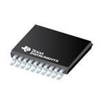
| 描述 | IC 12-BIT 11CH SERIAL A/D 20SSOP模数转换器 - ADC 12bit ADC/3V |
| 产品分类 | |
| 品牌 | Texas Instruments |
| 产品手册 | |
| 产品图片 |
|
| rohs | 符合RoHS无铅 / 符合限制有害物质指令(RoHS)规范要求 |
| 产品系列 | 数据转换器IC,模数转换器 - ADC,Texas Instruments TLV2543IDB- |
| 数据手册 | |
| 产品型号 | TLV2543IDB |
| 产品培训模块 | http://www.digikey.cn/PTM/IndividualPTM.page?site=cn&lang=zhs&ptm=13240 |
| 产品目录页面 | |
| 产品种类 | 模数转换器 - ADC |
| 位数 | 12 |
| 供应商器件封装 | 20-SSOP |
| 信噪比 | Yes |
| 其它名称 | 296-2201-5 |
| 分辨率 | 12 bit |
| 制造商产品页 | http://www.ti.com/general/docs/suppproductinfo.tsp?distId=10&orderablePartNumber=TLV2543IDB |
| 包装 | 管件 |
| 单位重量 | 156.700 mg |
| 商标 | Texas Instruments |
| 安装类型 | 表面贴装 |
| 安装风格 | SMD/SMT |
| 封装 | Tube |
| 封装/外壳 | 20-SSOP(0.209",5.30mm 宽) |
| 封装/箱体 | SSOP-20 |
| 工作温度 | -40°C ~ 85°C |
| 工作电源电压 | 3 V to 3.6 V |
| 工厂包装数量 | 70 |
| 接口类型 | Serial |
| 数据接口 | 串行 |
| 最大工作温度 | + 85 C |
| 最小工作温度 | - 40 C |
| 标准包装 | 70 |
| 特性 | - |
| 电压参考 | External |
| 电压源 | 单电源 |
| 系列 | TLV2543 |
| 结构 | SAR |
| 转换器数 | 1 |
| 转换器数量 | 1 |
| 转换速率 | 66 kS/s |
| 输入数和类型 | 11 个单端,单极 |
| 输入类型 | Single-Ended |
| 通道数量 | 11 Channel |
| 配用 | /product-detail/zh/TLV2543EVM/296-10644-ND/379927 |
| 采样率(每秒) | 66k |


- 商务部:美国ITC正式对集成电路等产品启动337调查
- 曝三星4nm工艺存在良率问题 高通将骁龙8 Gen1或转产台积电
- 太阳诱电将投资9.5亿元在常州建新厂生产MLCC 预计2023年完工
- 英特尔发布欧洲新工厂建设计划 深化IDM 2.0 战略
- 台积电先进制程称霸业界 有大客户加持明年业绩稳了
- 达到5530亿美元!SIA预计今年全球半导体销售额将创下新高
- 英特尔拟将自动驾驶子公司Mobileye上市 估值或超500亿美元
- 三星加码芯片和SET,合并消费电子和移动部门,撤换高东真等 CEO
- 三星电子宣布重大人事变动 还合并消费电子和移动部门
- 海关总署:前11个月进口集成电路产品价值2.52万亿元 增长14.8%


PDF Datasheet 数据手册内容提取
TLV2543C, TLV2543I 12-BIT ANALOG-TO-DIGITAL CONVERTERS WITH SERIAL CONTROL AND 11 ANALOG INPUTS SLAS096C – MARCH 1995 – REVISED JUNE 2000 (cid:0) 12-Bit-Resolution A/D Converter (cid:0) 10-m s Conversion Time Over Operating DB, DW, OR N PACKAGE (TOP VIEW) Temperature Range (cid:0) 11 Analog Input Channels AIN0 1 20 VCC (cid:0) 3 Built-In Self-Test Modes AIN1 2 19 EOC (cid:0) Inherent Sample and Hold Function AIN2 3 18 I/O CLOCK (cid:0) Linearity Error...±1 LSB Max AIN3 4 17 DATA INPUT (cid:0) AIN4 5 16 DATA OUT On-Chip System Clock AIN5 6 15 CS (cid:0) End-of-Conversion (EOC) Output AIN6 7 14 REF+ (cid:0) Unipolar or Bipolar Output Operation AIN7 8 13 REF– (Signed Binary With Respect to Half of the AIN8 9 12 AIN10 Applied Referenced Voltage) GND 10 11 AIN9 (cid:0) Programmable MSB or LSB First (cid:0) Programmable Power Down (cid:0) Programmable Output Data Length (cid:0) CMOS Technology description The TLV2543C and TLV2543I are 12-bit, switched-capacitor, successive-approximation, analog-to-digital converters (ADCs). Each device has three control inputs [chip select (CS), the input-output clock (I/O CLOCK), and the address input (DATA INPUT)] and is designed for communication with the serial port of a host processor or peripheral through a serial 3-state output. The device allows high-speed data transfers from the host. In addition to the high-speed converter and versatile control capability, the device has an on-chip 14-channel multiplexer that can select any one of 11 inputs or any one of three internal self-test voltages. The sample-and-hold function is automatic. At the end of conversion, the end-of-conversion (EOC) output goes high to indicate that conversion is complete. The converter incorporated in the device features differential high-impedance reference inputs that facilitate ratiometric conversion, scaling, and isolation of analog circuitry from logic and supply noise. A switched-capacitor design allows low-error conversion over the full operating temperature range. The TLV2543 is available in the DW, DB, and N packages. The TLV2543C is characterized for operation from 0°C to 70°C, and the TLV2543I is characterized for operation from –40°C to 85°C. AVAILABLE OPTIONS PACKAGE TAA SMALL OUTLINE PLASTIC DIP DW† DB† N 0°C to 70°C TLV2543CDW TLV2543CDB TLV2543CN –40°C to 85°C TLV2543IDW TLV2543IDB TLV2543IN †Available in tape and reel and ordered as the TLV2543CDWR, TLV2543CDBLE, TLV2543IDBR, or TLV2543IDWR. Please be aware that an important notice concerning availability, standard warranty, and use in critical applications of TexasInstruments semiconductor products and disclaimers thereto appears at the end of this data sheet. PRODUCTION DATA information is current as of publication date. Copyright 2000, Texas Instruments Incorporated Products conform to specifications per the terms of Texas Instruments standard warranty. Production processing does not necessarily include testing of all parameters. POST OFFICE BOX 655303 • DALLAS, TEXAS 75265 1
TLV2543C, TLV2543I 12-BIT ANALOG-TO-DIGITAL CONVERTERS WITH SERIAL CONTROL AND 11 ANALOG INPUTS SLAS096C – MARCH 1995 – REVISED JUNE 2000 functional block diagram REF+ REF– 14 13 1 12-Bit AIN0 Sample and Analog-to-Digital 2 AIN1 Hold Converter 3 AIN2 (switched capacitors) 4 AIN3 5 AIN4 AIN5 6 14-Channel 12 7 Analog AIN6 Multiplexer 8 AIN7 AIN8 9 ODuatptaut 12 S1e2l-etoc-t1o rD aantad 16 DATA AIN9 11 4 Register Driver OUT 12 Input Address AIN10 Register 4 3 Control Logic Self-Test and I/O Reference Counters 19 EOC DATA 17 INPUT 18 I/O CLOCK 15 CS 2 POST OFFICE BOX 655303 • DALLAS, TEXAS 75265
TLV2543C, TLV2543I 12-BIT ANALOG-TO-DIGITAL CONVERTERS WITH SERIAL CONTROL AND 11 ANALOG INPUTS SLAS096C – MARCH 1995 – REVISED JUNE 2000 Terminal Functions TERMINAL II//OO DDEESSCCRRIIPPTTIIOONN NAME NO. AIN0 – AIN10 1–9, I Analog input. These 11 analog-signal inputs are internally multiplexed. The driving source impedance should 11, 12 be less than or equal to 50 W for 4.1-MHz I/O CLOCK operation and capable of slewing the analog input voltage into a capacitance of 60 pF. CS 15 I Chip select. A high-to-low transition on CS resets the internal counters and controls and enables DATA OUT, DATA INPUT, and I/O CLOCK. A low-to-high transition disables DATA INPUT and I/O CLOCK within a setup time. DATA INPUT 17 I Serial-data input. A 4-bit serial address selects the desired analog input or test voltage to be converted. The serial data is presented with the MSB first and is shifted in on the first four rising edges of I/O CLOCK. After the four address bits are read into the address register, I/O CLOCK clocks the remaining bits in order. DATA OUT 16 O Serial data output. This is the 3-state serial output for the A/D conversion result. DATA OUT is in the high-impedance state when CS is high and active when CS is low. With a valid CS, DATA OUT is removed from the high-impedance state and is driven to the logic level corresponding to the MSB/LSB value of the previous conversion result. The next falling edge of I/O CLOCK drives DATA OUT to the logic level corresponding to the next MSB/LSB, and the remaining bits are shifted out in order. EOC 19 O End of conversion. EOC goes from a high to a low logic level after the falling edge of the last I/O CLOCK and remains low until the conversion is complete and data are ready for transfer. GND 10 Ground. This is the ground return terminal for the internal circuitry. Unless otherwise noted, all voltage measurements are with respect to GND. I/O CLOCK 18 I Input/output clock. I/O CLOCK receives the serial input and performs the following four functions: 1. It clocks the eight input data bits into the input data register on the first eight rising edges of I/O CLOCK with the multiplexer address available after the fourth rising edge. 2. On the fourth falling edge of I/O CLOCK, the analog input voltage on the selected multiplexer input begins charging the capacitor array and continues to do so until the last falling edge of I/O CLOCK. 3. It shifts the 11 remaining bits of the previous conversion data out on DATA OUT. Data changes on the falling edge of I/O CLOCK. 4. It transfers control of the conversion to the internal state controller on the falling edge of the last I/O CLOCK. REF+ 14 I Reference+. The upper reference voltage value (nominally VCC) is applied to REF+. The maximum input voltage range is determined by the difference between the voltage applied to this terminal and the voltage applied to the REF– terminal. REF– 13 I Reference–. The lower reference voltage value (nominally ground) is applied to REF–. VCC 20 Positive supply voltage. detailed description Initially, with chip select (CS) high, I/O CLOCK and DATA INPUT are disabled and DATA OUT is in the high-impedance state. CS, going low, begins the conversion sequence by enabling I/O CLOCK and DATA INPUT and removes DATA OUT from the high-impedance state. The input data is an 8-bit data stream consisting of a 4-bit analog channel address (D7–D4), a 2-bit data length select (D3–D2), an output MSB or LSB first bit (D1), and a unipolar or bipolar output select bit (D0) that are applied to DATA INPUT. The I/O CLOCK sequence applied to the I/O CLOCK terminal transfers this data to the input data register. During this transfer, the I/O CLOCK sequence also shifts the previous conversion result from the output data register to DATA OUT. I/O CLOCK receives the input sequence of 8, 12, or 16 clocks long depending on the data-length selection in the input data register. Sampling of the analog input begins on the fourth falling edge of the input I/O CLOCK sequence and is held after the last falling edge of the I/O CLOCK sequence. The last falling edge of the I/O CLOCK sequence also takes EOC low and begins the conversion. POST OFFICE BOX 655303 • DALLAS, TEXAS 75265 3
TLV2543C, TLV2543I 12-BIT ANALOG-TO-DIGITAL CONVERTERS WITH SERIAL CONTROL AND 11 ANALOG INPUTS SLAS096C – MARCH 1995 – REVISED JUNE 2000 converter operation The operation of the converter is organized as a succession of two distinct cycles: 1) the I/O cycle, and 2) the actual conversion cycle. The I/O cycle is defined by the externally provided I/O CLOCK and lasts 8, 12, or 16 clock periods depending on the selected output data length. 1. I/O cycle During the I/O cycle, two operations take place simultaneously. a. An 8-bit data stream consisting of address and control information is provided to DATA INPUT. This data is shifted into the device on the rising edge of the first eight I/O CLOCKs. DATA INPUT is ignored after the first eight clocks during 12- or 16-clock I/O transfers. b. The data output with a length of 8, 12, or 16 bits is provided serially on DATA OUT. When CS is held low, the first output data bit occurs on the rising edge of EOC. When CS is negated between conversions, the first output data bit occurs on the falling edge of CS. This data is the result of the previous conversion period, and after the first output data bit each succeeding bit is clocked out on the falling edge of each succeeding I/O CLOCK. 2. Conversion cycle The conversion cycle is transparent to the user, and it is controlled by an internal clock synchronized to the I/O CLOCK. During the conversion period, the device performs a successive-approximation conversion on the analog input voltage. The EOC output goes low at the start of the conversion cycle and goes high when conversion is complete and the output data register is latched. A conversion cycle is started only after the I/O cycle is completed, which minimizes the influence of external digital noise on the accuracy of the conversion. power up and initialization After power up, CS must be taken from high to low to begin an I/O cycle. EOC is initially high, and the input data register is set to all zeros. The contents of the output data register are random, and the first conversion result should be ignored. To initialize during operation, CS is taken high and returned low to begin the next I/O cycle. The first conversion after the device has returned from the power-down state may not read accurately due to internal device settling. operational terminology Previous (N–1) conversion cycle The conversion cycle prior to the current I/O cycle. Current (N) I/O cycle The entire I/O CLOCK sequence that transfers address and control data into the data register and clocks the digital result from the previous conversion cycle from DATA OUT. The last falling edge of the clock in the I/O CLOCK sequence signifies the end of the current I/O cycle. Current (N) conversion cycle Immediately after the current I/O cycle, the current conversion cycle starts. When the current conversion cycle is complete, the current conversion result is loaded into the output register. Current (N) conversion result The result of the current conversion cycle that is serially shifted out during the next I/O cycle. Next (N+1) I/O cycle The I/O cycle after the current conversion cycle. Example: In the 12-bit mode, the result of the current conversion cycle is a 12-bit serial-data stream clocked out during the next I/O cycle. The current I/O cycle must be exactly 12 bits long to maintain synchronization, even when this corrupts the output data from the previous conversion. The current conversion begins immediately after the twelfth falling edge of the current I/O cycle. data input The data input is internally connected to an 8-bit serial-input address and control register. The register defines the operation of the converter and the output data length. The host provides the data word with the MSB first. Each data bit is clocked in on the rising edge of the I/O CLOCK sequence (see Table 1 for the data register format). 4 POST OFFICE BOX 655303 • DALLAS, TEXAS 75265
TLV2543C, TLV2543I 12-BIT ANALOG-TO-DIGITAL CONVERTERS WITH SERIAL CONTROL AND 11 ANALOG INPUTS SLAS096C – MARCH 1995 – REVISED JUNE 2000 data input (continued) Table 1. Input-Register Format INPUT DATA BYTE ADDRESS BITS L1 L0 LSBF BIP FFUUNNCCTTIIOONN SSEELLEECCTT D7 D6 D5 D4 D3 D2 D1 D0 (MSB) (LSB) Select input channel AIN0 0 0 0 0 AIN1 0 0 0 1 AIN2 0 0 1 0 AIN3 0 0 1 1 AIN4 0 1 0 0 AIN5 0 1 0 1 AIN6 0 1 1 0 AIN7 0 1 1 1 AIN8 1 0 0 0 AIN9 1 0 0 1 AIN10 1 0 1 0 Select test voltage (Vref+ – Vref–)/2 1 0 1 1 Vref– 1 1 0 0 Vref+ 1 1 0 1 Software power down 1 1 1 0 Output data length 8 bits 0 1 12 bits X 0 16 bits 1 1 Output data format MSB first 0 LSB first 1 Unipolar (binary) 0 Bipolar (BIP, 2s complement) 1 data input address bits The four MSBs (D7 – D4) of the data register address one of the 11 input channels, a reference-test voltage, or the power-down mode. The address bits affect the current conversion, which is the conversion that immediately follows the current I/O cycle. The reference voltage is nominally equal to V – V . ref+ ref– data output length The next two bits (D3 and D2) of the data register select the output data length. The data-length selection is valid for the current I/O cycle (the cycle in which the data is read). The data-length selection, which is valid for the current I/O cycle, allows device start-up without losing I/O synchronization. A data length of 8, 12, or 16 bits can be selected. Since the converter has 12-bit resolution, a data length of 12 bits is suggested. With D3 and D2 set to 00 or 10, the device is in the 12-bit data-length mode and the result of the current conversion is output as a 12-bit serial-data stream during the next I/O cycle. The current I/O cycle must be exactly 12 bits long for proper synchronization, even when this means corrupting the output data from a previous conversion. The current conversion is started immediately after the twelfth falling edge of the current I/O cycle. With bits D3 and D2 set to 11, the 16-bit data-length mode is selected, which allows convenient communication with 16-bit serial interfaces. In the 16-bit mode, the result of the current conversion is output as a 16-bit serial-data stream during the next I/O cycle with the four LSBs always set to 0 (pad bits). The current I/O cycle must be exactly 16 bits long to maintain synchronization even when this means corrupting the output data from the previous conversion. The current conversion is started immediately after the sixteenth falling edge of the current I/O cycle. POST OFFICE BOX 655303 • DALLAS, TEXAS 75265 5
TLV2543C, TLV2543I 12-BIT ANALOG-TO-DIGITAL CONVERTERS WITH SERIAL CONTROL AND 11 ANALOG INPUTS SLAS096C – MARCH 1995 – REVISED JUNE 2000 data output length (continued) With bits D3 and D2 set to 01, the 8-bit data-length mode is selected, which allows fast communication with 8-bit serial interfaces. In the 8-bit mode, the result of the current conversion is output as an 8-bit serial-data stream during the next I/O cycle. The current I/O cycle must be exactly 8 bits long to maintain synchronization, even when this means corrupting the output data from the previous conversion. The four LSBs of the conversion result are truncated and discarded. The current conversion is immediately started after the eighth falling edge of the current I/O cycle. Since D3 and D2 take effect on the current I/O cycle when the data length is programmed, there can be a conflict with the previous cycle when the data-word length is changed from one cycle to the next. This may occur when the data format is selected to be least significant bit first, since at the time the data length change becomes effective (six rising edges of I/O CLOCK), the previous conversion result has already started shifting out. In actual operation, when different data lengths are required within an application and the data length is changed between two conversions, no more than one conversion result can be corrupted and only when it is shifted out in LSB first format. sampling period During the sampling period, one of the analog inputs is internally connected to the capacitor array of the converter to store the analog input signal. The converter starts sampling the selected input immediately after the four address bits have been clocked into the input data register. Sampling starts on the fourth falling edge of I/O CLOCK. The converter remains in the sampling mode until the eighth, twelfth, or sixteenth falling edge of the I/O CLOCK depending on the data-length selection. After the EOC delay time from the last I/O CLOCK falling edge, the EOC output goes low indicating that the sampling period is over and the conversion period has begun. After EOC goes low, the analog input can be changed without affecting the conversion result. Since the delay from the falling edge of the last I/O CLOCK to EOC low is fixed, time-varying analog input signals can be digitized at a fixed rate without introducing systematic harmonic distortion or noise due to timing uncertainty. After the 8-bit data stream has been clocked in, DATA INPUT should be held at a fixed digital level until EOC goes high (indicating that the conversion is complete) to maximize the sampling accuracy and minimize the influence of external digital noise. data register, LSB first D1 in the input data register (LSB first) controls the direction of the output binary data transfer. When D1 is set to 0, the conversion result shifts out MSB first. When set to 1, the data shifts out LSB first. Selection of MSB first or LSB first always affects the next I/O cycle and not the current I/O cycle. When changing from one data direction to another, the current I/O cycle is never disrupted. data register, bipolar format D0 in the input data register controls the binary data format used to represent the conversion result. When D0 is set to 0, the conversion result is represented as unipolar (unsigned binary) data. Nominally, the conversion result of an input voltage equal to V is a code of all zeros (000...0), the conversion result of an input voltage ref– equal to V is a code of all ones (111...1), and the conversion result of (V + V )/2 is a code of a one ref+ ref+ ref– followed by zeros (100...0). When D0 is set to 1, the conversion result is represented as bipolar data (signed binary). Nominally, conversion of an input voltage equal to V is a code of a 1 followed by zeros (100...0), conversion of an input voltage ref– equal to V is a code of a 0 followed by all ones (011...1), and the conversion of (V + V )/2 is a code ref+ ref+ ref– of all zeros (000...0). The MSB is interpreted as the sign bit. The bipolar data format is related to the unipolar format in that the MSBs are always each other’s complement. Selection of the unipolar or bipolar format always affects the current conversion cycle, and the result is output during the next I/O cycle. When changing between unipolar and bipolar formats, the data output during the current I/O cycle is not affected. 6 POST OFFICE BOX 655303 • DALLAS, TEXAS 75265
TLV2543C, TLV2543I 12-BIT ANALOG-TO-DIGITAL CONVERTERS WITH SERIAL CONTROL AND 11 ANALOG INPUTS SLAS096C – MARCH 1995 – REVISED JUNE 2000 EOC output The EOC signal indicates the beginning and the end of conversion. In the reset state, EOC is always high. During the sampling period (beginning after the fourth falling edge of the I/O CLOCK sequence), EOC remains high until the internal sampling switch of the converter is safely opened. The opening of the sampling switch occurs after the eighth, twelfth, or sixteenth I/O CLOCK falling edge, depending on the data-length selection in the input data register. After the EOC signal goes low, the analog input signal can be changed without affecting the conversion result. The EOC signal goes high again after the conversion completes and the conversion result is latched into the output data register. The rising edge of EOC returns the converter to a reset state and a new I/O cycle begins. On the rising edge of EOC, the first bit of the current conversion result is on DATA OUT when CS is low. When CS is negated between conversions, the first bit of the current conversion result occurs at DATA OUT on the falling edge of CS. data format and pad bits D3 and D2 of the input data register determine the number of significant bits in the digital output that represent the conversion result. The LSB-first bit determines the direction of the data transfer while the BIP bit determines the arithmetic conversion. The numerical data is always justified toward the MSB in any output format. The internal conversion result is always 12 bits long. When an 8-bit data transfer is selected, the four LSBs of the internal result are discarded to provide a faster one-byte transfer. When a 12-bit transfer is used, all bits are transferred. When a 16-bit transfer is used, four LSB pad bits are always appended to the internal conversion result. In the LSB-first mode, four leading zeros are output. In the MSB-first mode, the last four bits output are zeros. When CS is held low continuously, the first data bit of the just completed conversion occurs on DATA OUT on the rising edge of EOC. When a new conversion is started after the last falling edge of I/O CLOCK, EOC goes low and the serial output is forced to a logic zero until EOC goes high again. When CS is negated between conversions, the first data bit occurs on DATA OUT on the falling edge of CS. On each subsequent falling edge of I/O CLOCK after the first data bit appears, the data is changed to the next bit in the serial conversion result until the required number of bits has been output. chip-select input (CS) The chip-select input (CS) enables and disables the device. During normal operation, CS should be low. Although the use of CS is not necessary to synchronize a data transfer, it can be brought high between conversions to coordinate the data transfer of several devices sharing the same bus. When CS is brought high, the serial-data output is immediately brought to the high-impedance state, releasing its output data line to other devices that may share it. After an internally generated debounce time, the I/O CLOCK is inhibited, thus preventing any further change in the internal state. When CS is subsequently brought low again, the device is reset. CS must be held low for an internal debounce time before the reset operation takes effect. After CS is debounced low, I/O CLOCK must remain inactive (low) for a minimum time before a new I/O cycle can start. CS can be used to interrupt any ongoing data transfer or any ongoing conversion. When CS is debounced low long enough before the end of the current conversion cycle, the previous conversion result is saved in the internal output buffer and then shifted out during the next I/O cycle. POST OFFICE BOX 655303 • DALLAS, TEXAS 75265 7
TLV2543C, TLV2543I 12-BIT ANALOG-TO-DIGITAL CONVERTERS WITH SERIAL CONTROL AND 11 ANALOG INPUTS SLAS096C – MARCH 1995 – REVISED JUNE 2000 power-down features When a binary address of 1110 is clocked into the input data register during the first four I/O CLOCK cycles, the power-down mode is selected. Power down is activated on the falling edge of the fourth I/O CLOCK pulse. During power down, all internal circuitry is put in a low-current standby mode. No conversions are performed, and the internal output buffer keeps the previous conversion cycle data results, provided that all digital inputs are held above V – 0.3 V or below 0.3 V. The I/O logic remains active so the current I/O cycle must be CC completed even when the power-down mode is selected. Upon power-on reset and before the first I/O cycle, the converter normally begins in the power-down mode. The device remains in the power-down mode until a valid (other than 1110) input address clocks in. Upon completion of that I/O cycle, a normal conversion is performed with the results being shifted out during the next I/O cycle. analog input, test, and power-down mode The 11 analog inputs, three internal voltages, and power-down mode are selected by the input multiplexer according to the input addresses shown in Tables 2, 3, and 4. The input multiplexer is a break-before-make type to reduce input-to-input noise rejection resulting from channel switching. Sampling of the analog input starts on the falling edge of the fourth I/O CLOCK and continues for the remaining I/O CLOCK pulses. The sample is held on the falling edge of the last I/O CLOCK pulse. The three internal test inputs are applied to the multiplexer, sampled, and converted in the same manner as the external analog inputs. The first conversion after the device has returned from the power-down state may not read accurately due to internal device settling. Table 2. Analog-Channel-Select Address VALUE SHIFTED INTO ANALOG INPUT DATA INPUT SSEELLEECCTTEEDD BINARY HEX AIN0 0000 0 AIN1 0001 1 AIN2 0010 2 AIN3 0011 3 AIN4 0100 4 AIN5 0101 5 AIN6 0110 6 AIN7 0111 7 AIN8 1000 8 AIN9 1001 9 AIN10 1010 A Table 3. Test-Mode-Select Address INTERNAL VALUE SHIFTED INTO SELF-TEST DATA INPUT UNIPOLAR OUTPUT VVOOLLTTAAGGEE RREESSUULLTT ((HHEEXX))‡‡ SELECTED† BINARY HEX Vref+ – Vref– 1011 B 200 2 Vref– 1100 C 000 Vref+ 1101 D 3FF †Vref+ is the voltage applied to REF+, and Vref– is the voltage applied to REF–. ‡The output results shown are the ideal values and may vary with the reference stability and with internal offsets. 8 POST OFFICE BOX 655303 • DALLAS, TEXAS 75265
TLV2543C, TLV2543I 12-BIT ANALOG-TO-DIGITAL CONVERTERS WITH SERIAL CONTROL AND 11 ANALOG INPUTS SLAS096C – MARCH 1995 – REVISED JUNE 2000 analog input, test, and power-down mode (continued) Table 4. Power-Down-Select Address VALUE SHIFTED INTO INPUT COMMAND DATA INPUT RESULT BINARY HEX Power down 1110 E ICC ≤ 25m A converter and analog input The CMOS threshold detector in the successive-approximation conversion system determines each bit by examining the charge on a series of binary-weighted capacitors (see Figure 1). In the first phase of the conversion process, the analog input is sampled by closing the S switch and all S switches simultaneously. C T This action charges all the capacitors to the input voltage. In the next phase of the conversion process, all S and S switches are opened and the threshold detector T C begins identifying bits by identifying the charge (voltage) on each capacitor relative to the reference (REF–) voltage. In the switching sequence, 12 capacitors are examined separately until all 12 bits are identified and the charge-convert sequence is repeated. In the first step of the conversion phase, the threshold detector looks at the first capacitor (weight = 4096). Node 4096 of this capacitor is switched to the REF+ voltage, and the equivalent nodes of all the other capacitors on the ladder are switched to REF–. When the voltage at the summing node is greater than the trip point of the threshold detector (approximately one-half V ), a bit 0 is CC placed in the output register and the 4096-weight capacitor is switched to REF–. When the voltage at the summing node is less than the trip point of the threshold detector, a bit 1 is placed in the register and the 4096-weight capacitor remains connected to REF+ through the remainder of the successive-approximation process. The process is repeated for the 2048-weight capacitor, the 1024-weight capacitor, and so forth down the line until all bits are determined. With each step of the successive-approximation process, the initial charge is redistributed among the capacitors. The conversion process relies on charge redistribution to determine the bits from MSB to LSB. SC Threshold Detector To Output 4096 2048 1024 16 8 4 2 1 1 Latches Node 4096 REF+ REF+ REF+ REF+ REF+ REF+ REF+ REF– REF– REF– REF– REF– REF– REF– REF– REF– ST ST ST ST ST ST ST ST ST VI Figure 1. Simplified Model of the Successive-Approximation System POST OFFICE BOX 655303 • DALLAS, TEXAS 75265 9
TLV2543C, TLV2543I 12-BIT ANALOG-TO-DIGITAL CONVERTERS WITH SERIAL CONTROL AND 11 ANALOG INPUTS SLAS096C – MARCH 1995 – REVISED JUNE 2000 reference voltage inputs There are two reference voltage inputs on the device, REF+ and REF–. The voltage values on these terminals establish the upper and lower limits of the analog input to produce a full-scale and zero-scale reading respectively. These voltages and the analog input should not exceed the positive supply or be lower than ground consistent with the specified absolute maximum ratings. The digital output is at full scale when the input signal is equal to or higher than REF+ terminal voltage and at zero when the input signal is equal to or lower than REF– terminal voltage. absolute maximum ratings over operating free-air temperature range (unless otherwise noted)† Supply voltage range, V (see Note 1) . . . . . . . . . . . . . . . . . . . . . . . . . . . . . . . . . . . . . . . . . . . . . –0.5 V to 6.5 V CC Input voltage range, V (any input) . . . . . . . . . . . . . . . . . . . . . . . . . . . . . . . . . . . . . . . . . . . . –0.3 V to V + 0.3 V I CC Output voltage range, V . . . . . . . . . . . . . . . . . . . . . . . . . . . . . . . . . . . . . . . . . . . . . . . . . . . –0.3 V to V + 0.3 V O CC Positive reference voltage, V . . . . . . . . . . . . . . . . . . . . . . . . . . . . . . . . . . . . . . . . . . . . . . . . . . . . . . V + 0.1 V ref+ CC Negative reference voltage, V . . . . . . . . . . . . . . . . . . . . . . . . . . . . . . . . . . . . . . . . . . . . . . . . . . . . . . . . . . –0.1 V ref– Peak input current, I (any input) . . . . . . . . . . . . . . . . . . . . . . . . . . . . . . . . . . . . . . . . . . . . . . . . . . . . . . . . . . ±20 mA I Peak total input current (all inputs) . . . . . . . . . . . . . . . . . . . . . . . . . . . . . . . . . . . . . . . . . . . . . . . . . . . . . . . . ±30 mA Operating free-air temperature range, T : TLV2543C . . . . . . . . . . . . . . . . . . . . . . . . . . . . . . . . . . . 0°C to 70°C A TLV2543I . . . . . . . . . . . . . . . . . . . . . . . . . . . . . . . . . . –40°C to 85°C Storage temperature range, T . . . . . . . . . . . . . . . . . . . . . . . . . . . . . . . . . . . . . . . . . . . . . . . . . . . –65°C to 150°C stg Lead temperature 1,6 mm (1/16 inch) from the case for 10 seconds . . . . . . . . . . . . . . . . . . . . . . . . . . . . 260°C †Stresses beyond those listed under “absolute maximum ratings” may cause permanent damage to the device. These are stress ratings only, and functional operation of the device at these or any other conditions beyond those indicated under “recommended operating conditions” is not implied. Exposure to absolute-maximum-rated conditions for extended periods may affect device reliability. NOTE 1: All voltage values are with respect to the GND terminal with REF– and GND wired together (unless otherwise noted). 10 POST OFFICE BOX 655303 • DALLAS, TEXAS 75265
TLV2543C, TLV2543I 12-BIT ANALOG-TO-DIGITAL CONVERTERS WITH SERIAL CONTROL AND 11 ANALOG INPUTS SLAS096C – MARCH 1995 – REVISED JUNE 2000 recommended operating conditions MIN NOM MAX UNIT Supply voltage, VCC 3 3.3 3.6 V Positive reference voltage, Vref+ (see Note 2) VCC V Negative reference voltage, Vref– (see Note 2) 0 V Differential reference voltage, Vref+ – Vref– (see Note 2) 2.5 VCC VCC+0.1 V Analog input voltage (see Note 2) 0 VCC V High-level control input voltage, VIH VCC = 3 V to 3.6 V 2.1 V Low-level control input voltage, VIL VCC = 3 V to 3.6 V 0.6 V Clock frequency at I/O CLOCK 0 3 4.1 MHz Setup time, address bits at DATA INPUT before I/O CLOCK↑, tsu(A) (see Figure 5) 100 ns Hold time, address bits at DATA INPUT after I/O CLOCK↑, th(A) (see Figure 5) 0 ns Hold time, CS low after last I/O CLOCK↓, th(CS) (see Figure 6) 0 ns Setup time, CS low before clocking in first address bit, tsu(CS) (see Note 3 and Figure 6) 1.425 m s Pulse duration, I/O CLOCK high, twH(I/O) 190 ns Pulse duration, I/O CLOCK low, twL(I/O) 190 ns Transition time, I/O CLOCK, tt(I/O) (see Note 4 and Figure 7) 1 m s Transition time, DATA INPUT and CS, tt(CS) 10 m s TLV2543C 0 70 OOppeerraattiinngg ffrreeee-aaiirr tteemmppeerraattuurree, TTAA °°CC TLV2543I –40 85 NOTES: 2. Analog input voltages greater than the voltage applied to REF+ convert as all ones (111111111111), while input voltages less than the voltage applied to REF– convert as all zeros (000000000000). 3. To minimize errors caused by noise at the CS input, the internal circuitry waits for a setup time after CS↓ before responding to control input signals. No attempt should be made to clock in an address until the minimum CS setup time elapses. 4. This is the time required for the clock input signal to fall from VIHmin to VILmax or to rise from VILmax to VIHmin. In the vicinity of normal room temperature, the devices function with input clock transition time as slow as 1 m s for remote data acquisition applications where the sensor and the A/D converter are placed several feet away from the controlling microprocessor. POST OFFICE BOX 655303 • DALLAS, TEXAS 75265 11
TLV2543C, TLV2543I 12-BIT ANALOG-TO-DIGITAL CONVERTERS WITH SERIAL CONTROL AND 11 ANALOG INPUTS SLAS096C – MARCH 1995 – REVISED JUNE 2000 electrical characteristics over recommended operating free-air temperature range, V = V = 3 V to 3.6 V (unless otherwise noted) CC ref+ PARAMETER TEST CONDITIONS MIN TYP† MAX UNIT VCC = 3 V, IOH = –0.2 mA 2.4 VVOOHH HHiigghh-lleevveell oouuttppuutt vvoollttaaggee VV VCC = 3 V to 3.6 V, IOH = –20 m A VCC–0.1 VCC = 3 V, IOL = 0.8 mA 0.4 VVOOLL LLooww-lleevveell oouuttppuutt vvoollttaaggee VV VCC = 3 V to 3.6 V, IOL = 20 m A 0.1 Off-state ((higgh-impedance-state)) VO = VCC, CS at VCC 1 2.5 IIOOZZ mm AA output current VO = 0, CS at VCC 1 –2.5 IIH High-level input current VI = VCC 1 2.5 m A IIL Low-level input current VI = 0 1 –2.5 m A ICC Operating supply current CS at 0 V 1 2.5 mA For all digital inputs, ICC(PD) Power-down current 0 ≤VI ≤ 0.3 V or VI ≥ VCC – 0.3 V 4 25 m A Selected channel leakagge Selected channel at VCC, Unselected channel at 0 V 1 IIllkkg mm AA current Selected channel at 0 V, Unselected channel at VCC –1 Maximum static analog reference current into REF+ Vref+ = VCC, Vref– = GND 1 2.5 m A Input Analog inputs 30 60 CCii capacitance Control inputs 5 15 ppFF †All typical values are at VCC = 5 V, TA = 25°C. 12 POST OFFICE BOX 655303 • DALLAS, TEXAS 75265
TLV2543C, TLV2543I 12-BIT ANALOG-TO-DIGITAL CONVERTERS WITH SERIAL CONTROL AND 11 ANALOG INPUTS SLAS096C – MARCH 1995 – REVISED JUNE 2000 operating characteristics over recommended operating free-air temperature range, V = V = 3 V to 3.6 V, I/O CLOCK frequency = 4.1 MHz, (unless otherwise noted) CC ref+ PARAMETER TEST CONDITIONS MIN TYP† MAX UNIT EL Linearity error (see Note 6) See Figure 2 ±1 LSB ED Differential linearity error See Figure 2 ±1 LSB EO Offset error (see Note 7) See Note 2 and ±1.5 LSB Figure 2 EG Gain error (see Note 7) See Note 2 and ±1 LSB Figure 2 ET Total unadjusted error (see Note 8) ±1.75 LSB DATA INPUT = 1011 2038 2048 2058 Self-test output code (see Table 3 and Note 9) DATA INPUT = 1100 0 10 DATA INPUT = 1101 4075 4095 t(conv) Conversion time See Figures 10–15 8 10 m s 10 + total See Figures 10–15 I/O CLOCK tc Total cycle time (access, sample, and conversion) and Note 10 periods + m s td(I/O-EOC) I/O See Figures 10–15 tacq Channel acquisition time (sample) and Note 10 4 12 CLOCK periods tv Valid time, DATA OUT remains valid after I/O CLOCK↓ See Figure 7 10 ns td(I/O-DATA) Delay time, I/O CLOCK↓ to DATA OUT valid See Figure 7 250 ns td(I/O-EOC) Delay time, last I/O CLOCK↓ to EOC↓ See Figure 8 1.5 2.2 m s td(EOC-DATA) Delay time, EOC↑ to DATA OUT (MSB/LSB) See Figure 9 200 ns tPZH, tPZL Enable time, CS↓ to DATA OUT (MSB/LSB driven) See Figure 4 0.7 1.3 m s tPHZ, tPLZ Disable time, CS↑ to DATA OUT (high impedance) See Figure 4 70 150 ns tr(EOC) Rise time, EOC See Figure 9 15 50 ns tf(EOC) Fall time, EOC See Figure 8 15 50 ns tr(bus) Rise time, data bus See Figure 7 15 50 ns tf(bus) Fall time, data bus See Figure 7 15 50 ns Delay time, last I/O CLOCK↓ to CS↓ to abort conversion td(I/O-CS) (see Note 11) 5 m s †All typical values are at TA = 25°C. NOTES: 2. Analog input voltages greater than that applied to REF+ convert as all ones (111111111111), while input voltages less than that applied to REF– convert as all zeros (000000000000). 6. Linearity error is the maximum deviation from the best straight line through the A/D transfer characteristics. 7. Gain error is the difference between the actual midstep value and the nominal midstep value in the transfer diagram at the specified gain point after the offset error has been adjusted to zero. Offset error is the difference between the actual midstep value and the nominal midstep value at the offset point. 8. Total unadjusted error comprises linearity, zero-scale, and full-scale errors. 9. Both the input address and the output codes are expressed in positive logic. 10. I/O CLOCK period = 1/(I/O CLOCK frequency) (see Figure 7). 11. Any transitions of CS are recognized as valid only when the level is maintained for a setup time. CS must be taken low at ≤ 5 m s of the tenth I/O CLOCK falling edge to ensure that a conversion is aborted. Between 5 m s and 10 m s, the result is uncertain as to whether the conversion is aborted or the conversion results are valid. POST OFFICE BOX 655303 • DALLAS, TEXAS 75265 13
TLV2543C, TLV2543I 12-BIT ANALOG-TO-DIGITAL CONVERTERS WITH SERIAL CONTROL AND 11 ANALOG INPUTS SLAS096C – MARCH 1995 – REVISED JUNE 2000 PARAMETER MEASUREMENT INFORMATION 15 V 50 W C1 C2 C3 10 m F 0.1 m F 470 pF TLV2543 _ 10 W U1 AIN0–AIN10 VI + C1 C2 C3 10 m F 0.1 m F 470 pF 50 W –15 V LOCATION DESCRIPTION PART NUMBER U1 OP27 — C1 10-m F 35-V tantalum capacitor — C2 0.1-m F ceramic NPO SMD capacitor AVX 12105C104KA105 or equivalent C3 470-pF porcelain high-Q SMD capacitor Johanson 201S420471JG4L or equivalent Figure 2. Analog Input Buffer to Analog Inputs AIN0–AIN10 Isource 0.8 mA Test Point See Note A Output Under Test Vcp = 2 V CL = 100 pF Isink –0.2 mA NOTE A: Equivalent load circuit of the Teradyne A580 tester for timing parameter measurement. Figure 3. Timing Load Circuits Data Valid 2 V 2 V CS 0.8 V DATA INPUT 0.8 V tPZH, tPZL tPHZ, tPLZ tsu(A) th(A) 2.4 V 90% DATA I/O CLOCK OUT 0.4 V 10% 0.8 V Figure 4. DATA OUT to Hi-Z Voltage Waveforms Figure 5. DATA INPUT and I/O CLOCK Voltage Waveforms 14 POST OFFICE BOX 655303 • DALLAS, TEXAS 75265
TLV2543C, TLV2543I 12-BIT ANALOG-TO-DIGITAL CONVERTERS WITH SERIAL CONTROL AND 11 ANALOG INPUTS SLAS096C – MARCH 1995 – REVISED JUNE 2000 PARAMETER MEASUREMENT INFORMATION 2 V CS 0.8 V tsu(CS) th(CS) I/O CLOCK Last 0.8 V 0.8 V Clock Figure 6. CS and I/O CLOCK Voltage Waveforms† †To ensure full conversion accuracy, it is recommended that no input signal change occurs while a conversion is ongoing. tt(I/O) tt(I/O) 2 V 2 V I/O CLOCK 0.8 V 0.8 V 0.8 V I/O CLOCK Period td(I/O-DATA) tv 2.4 V 2.4 V DATA OUT 0.4 V 0.4 V tr(bus), tf(bus) Figure 7. I/O CLOCK and DATA OUT Voltage Waveforms I/O CLOCK Last 0.8 V Clock td(I/O-EOC) EOC 2.4 V 0.4 V tf(EOC) Figure 8. I/O CLOCK and EOC Voltage Waveforms tr(EOC) EOC 2.4 V 0.4 V td(EOC-DATA) 2.4 V DATA OUT 0.4 V Valid MSB Figure 9. EOC and DATA OUT Voltage Waveforms POST OFFICE BOX 655303 • DALLAS, TEXAS 75265 15
TLV2543C, TLV2543I 12-BIT ANALOG-TO-DIGITAL CONVERTERS WITH SERIAL CONTROL AND 11 ANALOG INPUTS SLAS096C – MARCH 1995 – REVISED JUNE 2000 PARAMETER MEASUREMENT INFORMATION CS (see Note A) ÎÎÎÎÎÎ I/O 1 2 3 4 5 6 7 8 11 12 1 CLOCK ÎÎÎÎÎÎ Access Cycle B Sample Cycle B Hi-Z State DATA A11 A10 A9 A8 A7 A6 A5 A4 A1 A0 B11 OUT Previous Conversion Data MSB LSB ÎÎÎÎÎÎÎÎÎÎÎÎÎÎÎÎÎÎÎÎ ÎÎÎÎ DATA INPUÎT ÎÎÎÎÎÎÎÎÎÎÎÎÎÎÎÎÎÎÎ ÎÎÎÎ B7 B6 B5 B4 B3 B2 B1 B0 C7 MSB LSB EOC Shift in New Multiplexer Address, t(conv) Simultaneously Shift Out Previous Conversion Value A/D Conversion Interval Initialize Initialize Figure 10. Timing for 12-Clock Transfer Using CS With MSB First CS (see Note A) I/O 1 2 3 4 5 6 7 8 11 12 1 CLOCK Access Cycle B Sample Cycle B DATA A11 A10 A9 A8 A7 A6 A5 A4 A1 A0 Low Level B11 OUT Previous Conversion Data MSB LSB ÎÎÎÎÎÎÎÎÎÎÎÎÎÎÎÎÎÎÎÎ ÎÎÎÎ DATA ÎÎÎÎÎÎÎÎÎÎÎÎÎÎÎÎÎÎÎÎ ÎÎÎÎ INPUT B7 B6 B5 B4 B3 B2 B1 B0 C7 MSB LSB EOC Shift in New Multiplexer Address, t(conv) Simultaneously Shift Out Previous Conversion Value A/D Conversion Interval Initialize Initialize Figure 11. Timing for 12-Clock Transfer Not Using CS With MSB First NOTE A: To minimize errors caused by noise at CS, the internal circuitry waits for a setup time after CS↓ before responding to control input signals. Therefore, no attempt should be made to clock in an address until the minimum CS setup time has elapsed. 16 POST OFFICE BOX 655303 • DALLAS, TEXAS 75265
TLV2543C, TLV2543I 12-BIT ANALOG-TO-DIGITAL CONVERTERS WITH SERIAL CONTROL AND 11 ANALOG INPUTS SLAS096C – MARCH 1995 – REVISED JUNE 2000 PARAMETER MEASUREMENT INFORMATION CS (see Note A) ÎÎÎÎÎÎ I/O CLOCK 1 2 3 4 5 6 7 8 1 ÎÎÎÎÎÎ Access Cycle B Sample Cycle B Hi-Z DATA O UT A7 A6 A5 A4 A3 A2 A1 A0 B7 Previous Conversion Data MSB LSB ÎÎÎÎÎÎÎÎÎÎÎÎÎÎÎÎÎÎÎÎÎ ÎÎÎÎÎ DATA INPUT ÎÎÎÎÎÎÎÎÎÎÎÎÎÎÎÎÎÎÎÎÎ ÎÎÎÎÎ B7 B6 B5 B4 B3 B2 B1 B0 C7 MSB LSB EOC Shift in New Multiplexer Address, t(conv) Simultaneously Shift Out Previous Conversion Value A/D Conversion Interval Initialize Initialize Figure 12. Timing for 8-Clock Transfer Using CS With MSB First CS (see Note A) I/O CLOCK 1 2 3 4 5 6 7 8 1 Access Cycle B Sample Cycle B DATA OUT A7 A6 A5 A4 A3 A2 A1 A0 Low Level B7 Previous Conversion Data MSB LSB ÎÎÎÎÎÎÎÎÎÎÎ ÎÎÎÎÎ ÎÎÎÎÎ DATA INPUT ÎÎÎÎÎÎÎÎÎÎÎ ÎÎÎÎÎ ÎÎÎÎÎ B7 B6 B5 B4 B3 B2 B1 B0 C7 MSB LSB EOC Shift in New Multiplexer Address, t(conv) Simultaneously Shift Out Previous Conversion Value A/D Conversion Interval Initialize Initialize Figure 13. Timing for 8-Clock Transfer Not Using CS With MSB First NOTE A: To minimize errors caused by noise at CS, the internal circuitry waits for a setup time after CS↓ before responding to control input signals. Therefore, no attempt should be made to clock in an address until the minimum CS setup time has elapsed. POST OFFICE BOX 655303 • DALLAS, TEXAS 75265 17
TLV2543C, TLV2543I 12-BIT ANALOG-TO-DIGITAL CONVERTERS WITH SERIAL CONTROL AND 11 ANALOG INPUTS SLAS096C – MARCH 1995 – REVISED JUNE 2000 PARAMETER MEASUREMENT INFORMATION CS (see Note A) ÎÎÎÎÎÎ I/O 1 2 3 4 5 6 7 8 15 16 1 CLOCK ÎÎÎÎÎÎ Access Cycle B Sample Cycle B Hi-Z State DATA A15 A14 A13 A12 A11 A10 A9 A8 A1 A0 B15 OUT Previous Conversion Data MSB LSB ÎÎÎÎÎÎÎÎ Î ÎÎÎÎÎÎÎÎ ÎÎ DATAÎÎÎÎÎÎÎÎ Î ÎÎÎÎÎÎÎÎ ÎÎÎ INPUT B7 B6 B5 B4 B3 B2 B1 B0 C7 MSB LSB EOC Shift in New Multiplexer Address, t(conv) Simultaneously Shift Out Previous Conversion Value A/D Conversion Interval Initialize Initialize Figure 14. Timing for 16-Clock Transfer Using CS With MSB First CS (see Note A) I/O 1 2 3 4 5 6 7 8 15 16 1 CLOCK Access Cycle B Sample Cycle B DATA A15 A14 A13 A12 A11 A10 A9 A8 A1 A0 Low Level B15 OUT Previous Conversion Data MSB LSB ÎÎÎÎÎÎÎÎÎÎÎ ÎÎÎÎÎÎ ÎÎÎÎÎ DATA INPUT ÎÎÎÎÎÎÎÎÎÎÎ ÎÎÎÎÎÎ ÎÎÎÎÎ B7 B6 B5 B4 B3 B2 B1 B0 C7 MSB LSB EOC Shift in New Multiplexer Address, t(conv) Simultaneously Shift Out Previous Conversion Value A/D Conversion Interval Initialize Figure 15. Timing for 16-Clock Transfer Not Using CS With MSB First NOTE A: To minimize errors caused by noise at CS, the internal circuitry waits for a setup time after CS↓ before responding to control input signals. Therefore, no attempt should be made to clock in an address until the minimum CS setup time has elapsed. 18 POST OFFICE BOX 655303 • DALLAS, TEXAS 75265
TLV2543C, TLV2543I 12-BIT ANALOG-TO-DIGITAL CONVERTERS WITH SERIAL CONTROL AND 11 ANALOG INPUTS SLAS096C – MARCH 1995 – REVISED JUNE 2000 APPLICATION INFORMATION 111111111111 4095 See Notes A and B VFS 111111111110 4094 VFSnom 111111111101 4093 e VFT = VFS – 1/2 LSB od100000000001 2049 C ut p Outp100000000000 VZT = VZS + 1/2 LSB 2048 Ste al git 011111111111 2047 Di VZS 000000000010 2 000000000001 1 000000000000 0 4 6 0 00.0008 0.0016 1.6376 1.6384 1.6392 3.2752 5 3.2760 3.2768 0 7 0 2 0. 3. VI – Analog Input Voltage – V NOTES: A. This curve is based on the assumption that Vref+ and Vref– have been adjusted so that the voltage at the transition from digital 0 to 1 (VZT) is 0.0004 V and the transition to full scale (VFT) is 3.2756 V. 1 LSB = 0.8 mV. B. The full-scale value (VFS) is the step whose nominal midstep value has the highest absolute value. The zero-scale value (VZS) is the step whose nominal midstep value equals zero. Figure 16. Ideal Conversion Characteristics TLV2543 15 1 AIN0 CS 2 18 AIN1 I/O CLOCK 3 17 AIN2 DATA INPUT Control 4 Processor AIN3 Circuit 5 16 AIN4 DATA OUT Analog 6 19 Inputs 7 AIN5 EOC AIN6 8 AIN7 9 AIN8 14 11 REF+ 3-V DC Regulated AIN9 13 12 REF– AIN10 GND 10 To Source Ground Figure 17. Serial Interface POST OFFICE BOX 655303 • DALLAS, TEXAS 75265 19
TLV2543C, TLV2543I 12-BIT ANALOG-TO-DIGITAL CONVERTERS WITH SERIAL CONTROL AND 11 ANALOG INPUTS SLAS096C – MARCH 1995 – REVISED JUNE 2000 APPLICATIONS INFORMATION simplified analog input analysis Using the equivalent circuit in Figure 18, the time required to charge the analog input capacitance from 0 to V S within 1/2 LSB can be derived as follows: The capacitance charging voltage is given by VC(cid:1)VS(cid:3)1–e–tc(cid:2)RtCi(cid:4) (1) Where: R = R + r t s i The final voltage to 1/2 LSB is given by V (1/2 LSB) = V – (V /8192) (2) C S S Equating equation 1 to equation 2 and solving for time t gives c VS(cid:0)(cid:3)VS(cid:2)58192(cid:4)(cid:1)VS(cid:3)1–e–tc(cid:2)RtCi(cid:4) (3) and t (1/2 LSB) = R × C × ln(8192) (4) c t i Therefore, with the values given the time for the analog input signal to settle is t (1/2 LSB) = (R + 1 kW ) × 60 pF × ln(8192) (5) c s This time must be less than the converter sample time shown in the timing diagrams. Driving Source† TLV2543 Rs VI ri VS VC 1 kW MAX Ci 50 pF MAX VI = Input Voltage at AIN VS= External Driving Source Voltage Rs= Source Resistance ri = Input Resistance Ci = Input Capacitance †Driving source requirements: • Noise and distortion for the source must be equivalent to the resolution of the converter. • Rs must be real at the input frequency. Figure 18. Equivalent Input Circuit Including the Driving Source 20 POST OFFICE BOX 655303 • DALLAS, TEXAS 75265
TLV2543C, TLV2543I 12-BIT ANALOG-TO-DIGITAL CONVERTERS WITH SERIAL CONTROL AND 11 ANALOG INPUTS SLAS096C – MARCH 1995 – REVISED JUNE 2000 MECHANICAL DATA DB (R-PDSO-G**) PLASTIC SMALL-OUTLINE PACKAGE 28 PIN SHOWN 0,38 0,65 0,15 M 0,22 28 15 0,15 NOM 5,60 8,20 5,00 7,40 Gage Plane 1 14 0,25 A 0°–8° 1,03 0,63 Seating Plane 2,00 MAX 0,05 MIN 0,10 PINS ** 14 16 20 24 28 30 38 DIM A MAX 6,50 6,50 7,50 8,50 10,50 10,50 12,90 A MIN 5,90 5,90 6,90 7,90 9,90 9,90 12,30 4040065/B 10/94 NOTES: A. All linear dimensions are in millimeters. B. This drawing is subject to change without notice. C. Body dimensions do not include mold flash or protrusion not to exceed 0,15. D. Falls within JEDEC MO-150 POST OFFICE BOX 655303 • DALLAS, TEXAS 75265 21
TLV2543C, TLV2543I 12-BIT ANALOG-TO-DIGITAL CONVERTERS WITH SERIAL CONTROL AND 11 ANALOG INPUTS SLAS096C – MARCH 1995 – REVISED JUNE 2000 MECHANICAL DATA DW (R-PDSO-G**) PLASTIC SMALL-OUTLINE PACKAGE 16 PIN SHOWN PINS ** 0.050 (1,27) 16 20 24 28 DIM 0.020 (0,51) 0.010 (0,25) M 0.410 0.510 0.610 0.710 0.014 (0,35) A MAX (10,41) (12,95) (15,49) (18,03) 16 9 0.400 0.500 0.600 0.700 A MIN (10,16) (12,70) (15,24) (17,78) 0.419 (10,65) 0.400 (10,15) 0.299 (7,59) 0.010 (0,25) NOM 0.293 (7,45) Gage Plane 0.010 (0,25) 1 8 0°–8° 0.050 (1,27) A 0.016 (0,40) Seating Plane 0.012 (0,30) 0.004 (0,10) 0.104 (2,65) MAX 0.004 (0,10) 4040000/B 10/94 NOTES: A. All linear dimensions are in inches (millimeters). B. This drawing is subject to change without notice. C. Body dimensions do not include mold flash or protrusion not to exceed 0.006 (0,15). D. Falls within JEDEC MS-013 22 POST OFFICE BOX 655303 • DALLAS, TEXAS 75265
TLV2543C, TLV2543I 12-BIT ANALOG-TO-DIGITAL CONVERTERS WITH SERIAL CONTROL AND 11 ANALOG INPUTS SLAS096C – MARCH 1995 – REVISED JUNE 2000 MECHANICAL DATA N (R-PDIP-T**) PLASTIC DUAL-IN-LINE PACKAGE 16 PIN SHOWN A PINS ** 16 9 14 16 18 20 DIM 0.775 0.775 0.920 0.975 A MAX (19,69) (19,69) (23.37) (24,77) 0.260 (6,60) 0.240 (6,10) 0.745 0.745 0.850 0.940 A MIN (18,92) (18,92) (21.59) (23,88) 1 8 0.070 (1,78) MAX 0.310 (7,87) 0.035 (0,89) MAX 0.020 (0,51) MIN 0.290 (7,37) 0.200 (5,08) MAX Seating Plane 0.125 (3,18) MIN 0.100 (2,54) 0°–15° 0.021 (0,53) 0.010 (0,25) M 0.015 (0,38) 0.010 (0,25) NOM 14 Pin Only 4040049/C 7/95 NOTES: A. All linear dimensions are in inches (millimeters). B. This drawing is subject to change without notice. C. Falls within JEDEC MS-001 (20-pin package is shorter than MS-001) POST OFFICE BOX 655303 • DALLAS, TEXAS 75265 23
PACKAGE OPTION ADDENDUM www.ti.com 8-Jan-2007 PACKAGING INFORMATION OrderableDevice Status(1) Package Package Pins Package EcoPlan(2) Lead/BallFinish MSLPeakTemp(3) Type Drawing Qty TLV2543CDB ACTIVE SSOP DB 20 70 Green(RoHS& CUNIPDAU Level-1-260C-UNLIM noSb/Br) TLV2543CDBG4 ACTIVE SSOP DB 20 70 Green(RoHS& CUNIPDAU Level-1-260C-UNLIM noSb/Br) TLV2543CDBR ACTIVE SSOP DB 20 2000 Green(RoHS& CUNIPDAU Level-1-260C-UNLIM noSb/Br) TLV2543CDBRG4 ACTIVE SSOP DB 20 2000 Green(RoHS& CUNIPDAU Level-1-260C-UNLIM noSb/Br) TLV2543CDW ACTIVE SOIC DW 20 25 Green(RoHS& CUNIPDAU Level-1-260C-UNLIM noSb/Br) TLV2543CDWG4 ACTIVE SOIC DW 20 25 Green(RoHS& CUNIPDAU Level-1-260C-UNLIM noSb/Br) TLV2543CDWR ACTIVE SOIC DW 20 2000 Green(RoHS& CUNIPDAU Level-1-260C-UNLIM noSb/Br) TLV2543CDWRG4 ACTIVE SOIC DW 20 2000 Green(RoHS& CUNIPDAU Level-1-260C-UNLIM noSb/Br) TLV2543CN ACTIVE PDIP N 20 20 Pb-Free CUNIPDAU N/AforPkgType (RoHS) TLV2543CNE4 ACTIVE PDIP N 20 20 Pb-Free CUNIPDAU N/AforPkgType (RoHS) TLV2543IDB ACTIVE SSOP DB 20 70 Green(RoHS& CUNIPDAU Level-1-260C-UNLIM noSb/Br) TLV2543IDBG4 ACTIVE SSOP DB 20 70 Green(RoHS& CUNIPDAU Level-1-260C-UNLIM noSb/Br) TLV2543IDBR ACTIVE SSOP DB 20 2000 Green(RoHS& CUNIPDAU Level-1-260C-UNLIM noSb/Br) TLV2543IDBRG4 ACTIVE SSOP DB 20 2000 Green(RoHS& CUNIPDAU Level-1-260C-UNLIM noSb/Br) TLV2543IDW ACTIVE SOIC DW 20 25 Green(RoHS& CUNIPDAU Level-1-260C-UNLIM noSb/Br) TLV2543IDWG4 ACTIVE SOIC DW 20 25 Green(RoHS& CUNIPDAU Level-1-260C-UNLIM noSb/Br) TLV2543IDWR ACTIVE SOIC DW 20 2000 Green(RoHS& CUNIPDAU Level-1-260C-UNLIM noSb/Br) TLV2543IDWRG4 ACTIVE SOIC DW 20 2000 Green(RoHS& CUNIPDAU Level-1-260C-UNLIM noSb/Br) TLV2543IN ACTIVE PDIP N 20 20 Pb-Free CUNIPDAU N/AforPkgType (RoHS) TLV2543INE4 ACTIVE PDIP N 20 20 Pb-Free CUNIPDAU N/AforPkgType (RoHS) (1)Themarketingstatusvaluesaredefinedasfollows: ACTIVE:Productdevicerecommendedfornewdesigns. LIFEBUY:TIhasannouncedthatthedevicewillbediscontinued,andalifetime-buyperiodisineffect. NRND:Notrecommendedfornewdesigns.Deviceisinproductiontosupportexistingcustomers,butTIdoesnotrecommendusingthispartin anewdesign. PREVIEW:Devicehasbeenannouncedbutisnotinproduction.Samplesmayormaynotbeavailable. OBSOLETE:TIhasdiscontinuedtheproductionofthedevice. (2)EcoPlan-Theplannedeco-friendlyclassification:Pb-Free(RoHS),Pb-Free(RoHSExempt),orGreen(RoHS&noSb/Br)-pleasecheck http://www.ti.com/productcontentforthelatestavailabilityinformationandadditionalproductcontentdetails. Addendum-Page1
PACKAGE OPTION ADDENDUM www.ti.com 8-Jan-2007 TBD:ThePb-Free/Greenconversionplanhasnotbeendefined. Pb-Free(RoHS):TI'sterms"Lead-Free"or"Pb-Free"meansemiconductorproductsthatarecompatiblewiththecurrentRoHSrequirements forall6substances,includingtherequirementthatleadnotexceed0.1%byweightinhomogeneousmaterials.Wheredesignedtobesoldered athightemperatures,TIPb-Freeproductsaresuitableforuseinspecifiedlead-freeprocesses. Pb-Free(RoHSExempt):ThiscomponenthasaRoHSexemptionforeither1)lead-basedflip-chipsolderbumpsusedbetweenthedieand package, or 2) lead-based die adhesive used between the die and leadframe. The component is otherwise considered Pb-Free (RoHS compatible)asdefinedabove. Green(RoHS&noSb/Br):TIdefines"Green"tomeanPb-Free(RoHScompatible),andfreeofBromine(Br)andAntimony(Sb)basedflame retardants(BrorSbdonotexceed0.1%byweightinhomogeneousmaterial) (3) MSL, Peak Temp. -- The Moisture Sensitivity Level rating according to the JEDEC industry standard classifications, and peak solder temperature. Important Information and Disclaimer:The information provided on this page represents TI's knowledge and belief as of the date that it is provided. TI bases its knowledge and belief on information provided by third parties, and makes no representation or warranty as to the accuracy of such information. Efforts are underway to better integrate information from third parties. TI has taken and continues to take reasonable steps to provide representative and accurate information but may not have conducted destructive testing or chemical analysis on incomingmaterialsandchemicals.TIandTIsuppliersconsidercertaininformationtobeproprietary,andthusCASnumbersandotherlimited informationmaynotbeavailableforrelease. InnoeventshallTI'sliabilityarisingoutofsuchinformationexceedthetotalpurchasepriceoftheTIpart(s)atissueinthisdocumentsoldbyTI toCustomeronanannualbasis. Addendum-Page2
PACKAGE MATERIALS INFORMATION www.ti.com 9-Apr-2009 TAPE AND REEL INFORMATION *Alldimensionsarenominal Device Package Package Pins SPQ Reel Reel A0(mm) B0(mm) K0(mm) P1 W Pin1 Type Drawing Diameter Width (mm) (mm) Quadrant (mm) W1(mm) TLV2543CDBR SSOP DB 20 2000 330.0 16.4 8.2 7.5 2.5 12.0 16.0 Q1 TLV2543IDBR SSOP DB 20 2000 330.0 16.4 8.2 7.5 2.5 12.0 16.0 Q1 PackMaterials-Page1
PACKAGE MATERIALS INFORMATION www.ti.com 9-Apr-2009 *Alldimensionsarenominal Device PackageType PackageDrawing Pins SPQ Length(mm) Width(mm) Height(mm) TLV2543CDBR SSOP DB 20 2000 346.0 346.0 33.0 TLV2543IDBR SSOP DB 20 2000 346.0 346.0 33.0 PackMaterials-Page2
IMPORTANTNOTICE TexasInstrumentsIncorporatedanditssubsidiaries(TI)reservetherighttomakecorrections,modifications,enhancements,improvements, andotherchangestoitsproductsandservicesatanytimeandtodiscontinueanyproductorservicewithoutnotice.Customersshould obtainthelatestrelevantinformationbeforeplacingordersandshouldverifythatsuchinformationiscurrentandcomplete.Allproductsare soldsubjecttoTI’stermsandconditionsofsalesuppliedatthetimeoforderacknowledgment. TIwarrantsperformanceofitshardwareproductstothespecificationsapplicableatthetimeofsaleinaccordancewithTI’sstandard warranty.TestingandotherqualitycontroltechniquesareusedtotheextentTIdeemsnecessarytosupportthiswarranty.Exceptwhere mandatedbygovernmentrequirements,testingofallparametersofeachproductisnotnecessarilyperformed. TIassumesnoliabilityforapplicationsassistanceorcustomerproductdesign.Customersareresponsiblefortheirproductsand applicationsusingTIcomponents.Tominimizetherisksassociatedwithcustomerproductsandapplications,customersshouldprovide adequatedesignandoperatingsafeguards. TIdoesnotwarrantorrepresentthatanylicense,eitherexpressorimplied,isgrantedunderanyTIpatentright,copyright,maskworkright, orotherTIintellectualpropertyrightrelatingtoanycombination,machine,orprocessinwhichTIproductsorservicesareused.Information publishedbyTIregardingthird-partyproductsorservicesdoesnotconstitutealicensefromTItousesuchproductsorservicesora warrantyorendorsementthereof.Useofsuchinformationmayrequirealicensefromathirdpartyunderthepatentsorotherintellectual propertyofthethirdparty,oralicensefromTIunderthepatentsorotherintellectualpropertyofTI. ReproductionofTIinformationinTIdatabooksordatasheetsispermissibleonlyifreproductioniswithoutalterationandisaccompanied byallassociatedwarranties,conditions,limitations,andnotices.Reproductionofthisinformationwithalterationisanunfairanddeceptive businesspractice.TIisnotresponsibleorliableforsuchaltereddocumentation.Informationofthirdpartiesmaybesubjecttoadditional restrictions. ResaleofTIproductsorserviceswithstatementsdifferentfromorbeyondtheparametersstatedbyTIforthatproductorservicevoidsall expressandanyimpliedwarrantiesfortheassociatedTIproductorserviceandisanunfairanddeceptivebusinesspractice.TIisnot responsibleorliableforanysuchstatements. TIproductsarenotauthorizedforuseinsafety-criticalapplications(suchaslifesupport)whereafailureoftheTIproductwouldreasonably beexpectedtocauseseverepersonalinjuryordeath,unlessofficersofthepartieshaveexecutedanagreementspecificallygoverning suchuse.Buyersrepresentthattheyhaveallnecessaryexpertiseinthesafetyandregulatoryramificationsoftheirapplications,and acknowledgeandagreethattheyaresolelyresponsibleforalllegal,regulatoryandsafety-relatedrequirementsconcerningtheirproducts andanyuseofTIproductsinsuchsafety-criticalapplications,notwithstandinganyapplications-relatedinformationorsupportthatmaybe providedbyTI.Further,BuyersmustfullyindemnifyTIanditsrepresentativesagainstanydamagesarisingoutoftheuseofTIproductsin suchsafety-criticalapplications. TIproductsareneitherdesignednorintendedforuseinmilitary/aerospaceapplicationsorenvironmentsunlesstheTIproductsare specificallydesignatedbyTIasmilitary-gradeor"enhancedplastic."OnlyproductsdesignatedbyTIasmilitary-grademeetmilitary specifications.BuyersacknowledgeandagreethatanysuchuseofTIproductswhichTIhasnotdesignatedasmilitary-gradeissolelyat theBuyer'srisk,andthattheyaresolelyresponsibleforcompliancewithalllegalandregulatoryrequirementsinconnectionwithsuchuse. TIproductsareneitherdesignednorintendedforuseinautomotiveapplicationsorenvironmentsunlessthespecificTIproductsare designatedbyTIascompliantwithISO/TS16949requirements.Buyersacknowledgeandagreethat,iftheyuseanynon-designated productsinautomotiveapplications,TIwillnotberesponsibleforanyfailuretomeetsuchrequirements. FollowingareURLswhereyoucanobtaininformationonotherTexasInstrumentsproductsandapplicationsolutions: Products Applications Amplifiers amplifier.ti.com Audio www.ti.com/audio DataConverters dataconverter.ti.com Automotive www.ti.com/automotive DLP®Products www.dlp.com Broadband www.ti.com/broadband DSP dsp.ti.com DigitalControl www.ti.com/digitalcontrol ClocksandTimers www.ti.com/clocks Medical www.ti.com/medical Interface interface.ti.com Military www.ti.com/military Logic logic.ti.com OpticalNetworking www.ti.com/opticalnetwork PowerMgmt power.ti.com Security www.ti.com/security Microcontrollers microcontroller.ti.com Telephony www.ti.com/telephony RFID www.ti-rfid.com Video&Imaging www.ti.com/video RF/IFandZigBee®Solutions www.ti.com/lprf Wireless www.ti.com/wireless MailingAddress:TexasInstruments,PostOfficeBox655303,Dallas,Texas75265 Copyright©2009,TexasInstrumentsIncorporated