ICGOO在线商城 > 集成电路(IC) > 数据采集 - 模数转换器 > ADS8413IBRGZT

 Datasheet下载
- 型号: ADS8413IBRGZT
- 制造商: Texas Instruments
- 库位|库存: xxxx|xxxx
- 要求:
| 数量阶梯 | 香港交货 | 国内含税 |
| +xxxx | $xxxx | ¥xxxx |
查看当月历史价格
查看今年历史价格
ADS8413IBRGZT产品简介:
ICGOO电子元器件商城为您提供ADS8413IBRGZT由Texas Instruments设计生产,在icgoo商城现货销售,并且可以通过原厂、代理商等渠道进行代购。 ADS8413IBRGZT价格参考¥230.42-¥362.43。Texas InstrumentsADS8413IBRGZT封装/规格:数据采集 - 模数转换器, 16 Bit Analog to Digital Converter 1 Input 1 SAR 48-VQFN (7x7)。您可以下载ADS8413IBRGZT参考资料、Datasheet数据手册功能说明书,资料中有ADS8413IBRGZT 详细功能的应用电路图电压和使用方法及教程。
Texas Instruments 的 ADS8413IBRGZT 是一款高性能、16位、1兆采样/秒(MSPS)的模数转换器(ADC),广泛应用于需要高精度和高速数据采集的场景。其主要应用场景包括:

1. 工业自动化与过程控制:用于传感器信号的高精度采集,如温度、压力、流量等模拟信号的数字化处理,适用于PLC、智能仪表等设备。

2. 测试与测量设备:如示波器、频谱分析仪、数据记录仪等,利用其高分辨率和高速特性进行精确信号分析。

3. 医疗成像设备:用于CT、MRI或超声波设备中对微弱模拟信号进行快速、精确的数字化处理。

4. 通信系统:在无线基站、软件无线电(SDR)等设备中用于接收端的信号采集和处理。

5. 电力监测系统:用于电能质量分析仪、继电保护装置等,实现对电压、电流信号的实时监测与分析。

6. 精密数据采集系统(DAQ):适用于科研实验、实验室仪器等对信号保真度要求较高的场合。

ADS8413IBRGZT具备低功耗、宽输入范围、内置参考电压等特点,适合多种高精度、中高速度的应用需求。
| 参数 | 数值 |
| 产品目录 | 集成电路 (IC) |
| 描述 | IC ADC 16BIT 2MSPS 48-VQFN |
| 产品分类 | |
| 品牌 | Texas Instruments |
| 数据手册 | |
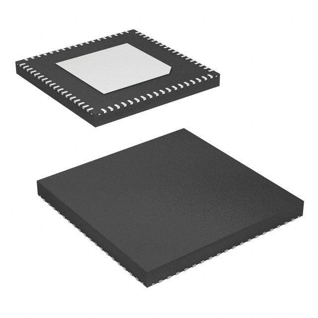
| 产品图片 |
|
| 产品型号 | ADS8413IBRGZT |
| PCN封装 | |
| rohs | 无铅 / 符合限制有害物质指令(RoHS)规范要求 |
| 产品系列 | - |
| 产品培训模块 | http://www.digikey.cn/PTM/IndividualPTM.page?site=cn&lang=zhs&ptm=13240 |
| 位数 | 16 |
| 供应商器件封装 | 48-VQFN(7x7) |
| 其它名称 | 296-19396-1 |
| 制造商产品页 | http://www.ti.com/general/docs/suppproductinfo.tsp?distId=10&orderablePartNumber=ADS8413IBRGZT |
| 包装 | Digi-Reel® |
| 安装类型 | 表面贴装 |
| 封装/外壳 | 48-VFQFN 裸露焊盘 |
| 工作温度 | -40°C ~ 85°C |
| 数据接口 | 串行 |
| 标准包装 | 1 |
| 特性 | - |
| 电压源 | 模拟和数字 |
| 转换器数 | 1 |
| 输入数和类型 | 1 个差分,单极 |
| 采样率(每秒) | 2M |


- 商务部:美国ITC正式对集成电路等产品启动337调查
- 曝三星4nm工艺存在良率问题 高通将骁龙8 Gen1或转产台积电
- 太阳诱电将投资9.5亿元在常州建新厂生产MLCC 预计2023年完工
- 英特尔发布欧洲新工厂建设计划 深化IDM 2.0 战略
- 台积电先进制程称霸业界 有大客户加持明年业绩稳了
- 达到5530亿美元!SIA预计今年全球半导体销售额将创下新高
- 英特尔拟将自动驾驶子公司Mobileye上市 估值或超500亿美元
- 三星加码芯片和SET,合并消费电子和移动部门,撤换高东真等 CEO
- 三星电子宣布重大人事变动 还合并消费电子和移动部门
- 海关总署:前11个月进口集成电路产品价值2.52万亿元 增长14.8%


PDF Datasheet 数据手册内容提取
(cid:2)(cid:17)(cid:14)(cid:14)(cid:20)(cid:2)(cid:14)(cid:13)(cid:18)(cid:12)(cid:0)(cid:4)(cid:14)(cid:13)(cid:8)(cid:17)(cid:7)(cid:16)(cid:15) (cid:10)(cid:14)(cid:13)(cid:11)(cid:0)(cid:5)(cid:9)(cid:19)(cid:6)(cid:15)(cid:0) (cid:3)(cid:12)(cid:15)(cid:16)(cid:14)(cid:17)(cid:11)(cid:9)(cid:12)(cid:16)(cid:15) ADS8413 SLAS490–OCTOBER2005 16-BIT, 2-MSPS, LVDS SERIAL INTERFACE, SAR ANALOG-TO-DIGITAL CONVERTER FEATURES APPLICATIONS • 2-MHzSampleRate • MedicalInstrumentation • 16-BitResolution • HIgh-SpeedDataAcquisitonSystems • SNR92dBat10kHzI/P • High-SpeedClose-LoopSystems • THD–107dBat10kHzI/P • Communication • – 1LSBTyp,– 2LSBINLMax DESCRIPTION • +0.7/–0.5LSBTyp,+1.5/–1LSBDNLMax The ADS8413 is a 16-bit, 2-MSPS, analog-to-digital • UnipolarDifferentialInputRange:–4V (A/D) converter with 4-V internal reference. The to4V device includes a capacitor based SAR A/D converter • InternalReference withinherentsampleandhold. • InternalReferenceBuffer The ADS8413 also includes a 200-Mbps, LVDS, • 200-MbpsLVDSSerialInterface serial interface. This interface is designed to support • Optional200-MHzInternalInterfaceClock daisy chaining or cascading of multiple devices. A selectable 16-/8-bit data frame mode enables the use • 16-/8-BitDataFrame of a single shift register chip (SN65LVDS152) for • ZeroLatencyatFullSpeed convertingthedatatoparallelformat. • PowerDissipation:290mWat2MSPS The ADS8413 unipolar differential input range • NapMode(125mWPowerDissipation) supportsadifferentialinputswingof–V to+V with ref ref • PowerDown(5m W) acommon-modevoltageof+Vref/2. • 48-PinQFNPackage The nap feature provides substantial power saving whenusedatlowerconversionrates. TheADS8413isavailableina48-pinQFNpackage. High-SpeedSARConverterFamily Type/Speed 500kHz ~600kHz 750kHZ 1MHz 1.25MHz 2MHz 3MHz 4MHz ADS8383 ADS8381 18-BitPseudo-Diff ADS8380(S) 18-BitPseudo-Bipolar,FullyDiff ADS8382(S) ADS8411 16-BitPseudo-Diff ADS8370(S) ADS8371 ADS8401/05 ADS8410 (S-LVDS) ADS8412 16-BitPseudo-Bipolar,FullyDiff ADS8372(S) ADS8402/06 ADS8413 (S-LVDS) 14-BitPseudo-Diff ADS7890(S) ADS7891 12-BitPseudo-Diff ADS7881 Pleasebeawarethatanimportantnoticeconcerningavailability,standardwarranty,anduseincriticalapplicationsofTexas Instrumentssemiconductorproductsanddisclaimerstheretoappearsattheendofthisdatasheet. PRODUCTIONDATAinformationiscurrentasofpublicationdate. Copyright©2005,TexasInstrumentsIncorporated Products conform to specifications per the terms of the Texas Instruments standard warranty. Production processing does not necessarilyincludetestingofallparameters.
ADS8413 www.ti.com SLAS490–OCTOBER2005 + VA AGND + VBD BDGND Core Supply I/O Supply SAR CSTART LVDS I/O SYNC_O, CLK_O, SDO SYNC_I, CLK_I, SDI + IN + CDAC − IN − CONVST Comparator BUS BUSY CMOS I/O RD REFIN Conversion BUSY Clock and CS Control Logic LAT_Y/N 4 V Internal Mode BYTE, REFOUT Reference Selection MODE_C/D, CLK_I/E, PD, NAP ORDERINGINFORMATION(1) MAXIMUM MAXIMUM NOMISSING TRANSPORT INTEGRAL DIFFERENTIAL CODESAT PACKAGE PACKAGE TEMPERATURE ORDERING MODEL MEDIA LINEARITY LINEARITY RESOLUTION TYPE DESIGNATOR RANGE INFORMATION QUANTITY (LSB) (LSB) (BIT) ADS8413lB – 2 1.5/–1 16 4Q8FpNin RGZ to–4805(cid:176)(cid:176)CC AADDSS88441133IIBBRRGGZZRT 2205000 ADS8413l – 4 3/–1 16 4Q8FpNin RGZ to–4805(cid:176)(cid:176)CC AADDSS88441133IIRRGGZZRT 2205000 (1) Forthemostcurrentpackageandorderinginformation,seethePackageOptionAddendumattheendofthisdocument,orseetheTI websiteatwww.ti.com. ABSOLUTE MAXIMUM RATINGS overoperatingfree-airtemperaturerange(unlessotherwisenoted)(1) UNIT +INtoAGND –0.3Vto+VA+0.3V -INtoAGND –0.3Vto+VA+0.3V +VAtoAGND –0.3to7V +VBDtoBDGND –0.3to7V DigitalinputvoltagetoGND –0.3Vto(+VBD+0.3V) DigitaloutputtoGND –0.3Vto(+VBD+0.3V) Operatingtemperaturerange –40(cid:176) Cto85(cid:176) C Storagetemperaturerange –65(cid:176) Cto150(cid:176) C Junctiontemperature(Tmax) 150(cid:176) C J Powerdissipation (T Max–T )/q J A JA QFNpackage q Thermalimpedance 86(cid:176) C/W JA Vaporphase(60sec) 215(cid:176) C Leadtemperature,soldering Infrared(15sec) 220(cid:176) C (1) Stressesbeyondthoselistedunderabsolutemaximumratingsmaycausepermanentdamagetothedevice.Thesearestressratings only,andfunctionaloperationofthedeviceattheseoranyotherconditionsbeyondthoseindicatedunderrecommendedoperating conditionsisnotimplied.Exposuretoabsolute-maximum-ratedconditionsforextendedperiodsmayaffectdevicereliability. 2
ADS8413 www.ti.com SLAS490–OCTOBER2005 SPECIFICATIONS T =–40(cid:176) Cto85(cid:176) C,+VA=5V,+VBD=5Vor3.3V,V =4.096V,f =2MHz(unlessotherwisenoted) A ref sample PARAMETER TESTCONDITIONS MIN TYP MAX UNIT ANALOGINPUT Full-scaleinputvoltagespan(1) +IN–(–IN) –Vref Vref V +IN –0.2 Vref+0.2 Absoluteinputvoltagerange V –IN –0.2 Vref+0.2 Inputcommon-modevoltagerange Vref/2–0.2 Vref/2 Vref/2+0.2 V Ci Inputcapacitance 25 pF Inputleakagecurrent 500 pA SYSTEMPERFORMANCE Resolution 16 Bits ADS8413IB 16 Nomissingcodes Bits ADS8413I 16 ADS8413IB –2 – 1 2 INL Integrallinearity(2) LSB(3) ADS8413I –4.0 – 2 4.0 ADS8413IB –1 0.7/–0.5 1.5 DNL Differentiallinearity LSB(3) ADS8413I –1.0 1.5/–0.8 3 ADS8413IB –1 – 0.2 1 EO Offseterror ADS8413I Externalreference –3.0 – 1 3.0 mV ADS8413IB –0.1 – 0.03 0.1 EG Gainerror(4) ADS8413I Externalreference –0.15 – 0.1 0.15 %ofFS Withcommonmodeinputsignal=200 CMMR Common-moderejectionratio 60 dB mVp-pat1MHz PSRR Powersupplyrejectionratio AtFFF0Houtputcode 80 dB SAMPLINGDYNAMICS +VBD=5V 360 391 Conversiontime ns +VBD=3V 391 +VBD=5V 100 Acquisitiontime ns +VBD=3V 100 Maximumthroughputratewithorwithoutlatency 2.0 MHz Aperturedelay 20 ns Aperturejitter 10 psec Stepresponse 50 ns Overvoltagerecovery 50 ns DYNAMICCHARACTERISTICS VIN0.5dBbelowFSat10kHz –107 THD Totalharmonicdistortion(5) VIN0.5dBbelowFSat100kHz –95 dB VIN0.5dBbelowFSat0.5MHz –90 VIN0.5dBbelowFSat10kHz 92 SNR Signal-to-noiseratio VIN0.5dBbelowFSat100kHz 90 dB VIN0.5dBbelowFSat0.5MHz 89 VIN0.5dBbelowFSat10kHz 92 SINAD Signal-to-noiseanddistortion VIN0.5dBbelowFSat100kHz 86 dB VIN0.5dBbelowFSat0.5MHz 84 VIN0.5dBbelowFSat10kHz –113 SFDR Spuriousfreedynamicrange VIN0.5dBbelowFSat100kHz –98 dB VIN0.5dBbelowFSat0.5MHz –93 –3dBSmallsignalbandwidth 37.5 MHz (1) Idealinputspan;doesnotincludegainoroffseterror. (2) ThisisendpointINL,notbestfit. (3) Leastsignificantbit (4) Measuredrelativetoactualmeasuredreference. (5) Calculatedonthefirstnineharmonicsoftheinputfrequency. 3
ADS8413 www.ti.com SLAS490–OCTOBER2005 SPECIFICATIONS (continued) T =–40(cid:176) Cto85(cid:176) C,+VA=5V,+VBD=5Vor3.3V,V =4.096V,f =2MHz(unlessotherwisenoted) A ref sample PARAMETER TESTCONDITIONS MIN TYP MAX UNIT EXTERNALREFERENCEINPUT Inputvoltagerange,VREF 3.9 4.096 4.2 V Resistance(6) Tointernalreferencevoltage 500 kW INTERNALREFERENCEOUTPUT From95%(+VA),with1-m Fstorage 25 Start-uptime ms capacitoronREFOUTtoAGND Referencevoltagerange,Vref Atroomtemperature 4.080 4.096 4.112 V Sourcecurrent Staticload 10 m A Lineregulation +VA=4.75Vto5.25V 0.6 mV Drift IOUT=0V 36 PPM/(cid:176)C POWERSUPPLYREQUIREMENTS +VBD 2.7 3.3 5.25 Powersupplyvoltage V +VA 4.75 5 5.25 Supplycurrent,2-MHzsamplerate +VA 58 64 mA Powerdissipation,2-MHzsamplerate +VA=5V 290 320 mW NAPMODE Supplycurrent +VA 25 mA POWERDOWN Supplycurrent +VA 1 2.5 m A Powerdowntime 10 m s With1-m Fstoragecapacitoron Poweruptime 25 ms REFOUTtoAGND Invalidconversionsafterpoweruporreset 3 Numbers TEMPERATURERANGE Operatingfreeair –40 85 (cid:176)C LOGICFAMILYCMOS VIH High-levelinputvoltage IIH=5m A +VBD–1 +VBD+0.3 V VIL Low-levelinputvoltage IIL=5m A –0.3 0.8 V VOH High-leveloutputvoltage IOH=2TTLloads +VBD–0.6 +VBD V VOL Low-leveloutputvoltage IOL=2TTLloads 0 0.4 V LOGICFAMILYLVDS(7) DRIVER Steady-statedifferentialoutputvoltage |VOD(SS)| magnitude 247 340 454 RL=100W ,SeeFigure52,Figure53 mV Changeinsteady-statedifferentialoutputvoltage -50 50 ∆|VOD(SS)| magnitudebetweenlogicstates VOC(SS) Steady-statecommon-modeoutputvoltage 1.125 1.2 1.375 V Changeinsteady-statecommon-modeoutput ∆|VOC(SS)| voltagebetweenlogicstates SeeFigure54 –50 50 mV Peaktopeakchangeincommon-modeoutput VOC(pp) voltage 50 150 VOYorVOZ=0V 3 10 IOS Shortcircuitoutputcurrent mA VOD=0V 3 10 IOZ Highimpedanceoutputcurrent VO=0Vor+VBD –5 5 m A (6) Canvary– 20% (7) Allminmaxvaluesensuredbydesign. 4
ADS8413 www.ti.com SLAS490–OCTOBER2005 SPECIFICATIONS (continued) T =–40(cid:176) Cto85(cid:176) C,+VA=5V,+VBD=5Vor3.3V,V =4.096V,f =2MHz(unlessotherwisenoted) A ref sample PARAMETER TESTCONDITIONS MIN TYP MAX UNIT RECEIVER VITH+ Positivegoingdifferentialvoltagethreshold 50 mV VITH- Negativegoingdifferentialvoltagethreshold –50 VIC Commonmodeinputvoltage 0.2 1.2 2.2 V CI Inputcapacitance 5 pF TIMING REQUIREMENTS T =–40(cid:176) Cto85(cid:176) C,+VA=5V,+VBD=5Vor3.3V(unlessotherwisenoted) A PARAMETER MIN TYP MAX UNIT REF SAMPLINGANDCONVERSIONRELATED Figure1, tacq Acquisitiontime 100 ns Figure2 Figure1, tcnv Conversiontime 391 ns Figure2 tw1 Pulseduration,CONVSThigh 100 ns Figure1 Figure1, tw2 Pulseduration,CONVSTlow 40 ns Figure2 td1 Delaytime,CONVSTrisingedgetosamplestart 5 ns Figure1 Figure1, td2 Delaytime,CONVSTfallingedgetoconversionstart 5 ns Figure2 +VBD=3.3V 14 Figure1, td3 Delaytime,CONVSTfallingedgetobusyhigh ns Figure2 +VBD=5V 13 +VBD=3.3V 8 Figure1, td4 Delaytime,conversionendtobusylow ns Figure2 +VBD=5V 7 Figure1, tw3 Pulseduration,CSTARThigh 100 ns Table2 Figure1, tw4 Pulseduration,CSTARTlow 45 ns Figure2, Table2 Figure1, td5 Delaytime,CSTARTrisingedgetosamplestart 7.5 ns Table2 Figure1, td6 Delaytime,CSTARTfallingedgetoconversionstart 7.5 ns Figure2, Table2 +VBD=3.3V 16.5 Figure1, td7 Delaytime,CSTARTfallingedgetobusyhigh ns Figure2, +VBD=5V 15.5 Table2 I/ORELATED td8 Delaytime,RDfallingedgewhileCSlowtoBUS_BUSYhigh 16 ns Figure5 Delaytime,RDfallingedgewhileCSlowtoSYNC_OandSDOoutof +VBD=3.3V 29 td9 3-statecondition(fordevicewithLAT_Y/Npulledlow) +VBD=5V 28 ns Figure5 Delaytime,pre_conversionend(pointA)toSYNC_OandSDOoutof3-state td10 condition 22 ns Figure6 VBD=3.3V 8 td11 Delaytime,pre_conversionend(pointA)toBUS_BUSYhigh ns Figure6 +VBD=5V 7 td12 Delaytime,conversionphaseendtoSYNC_Ohigh 6 9+tCLK ns Figure6 +VBD=3.3V 5.5+4*tCLK 8.5+5*tCLK td13 Delaytime,RDfallingedgewhileCSlowtoSYNC_Ohigh ns Figure5 +VBD=5V 5+4*tCLK 8+5*tCLK tw5 Pulseduration,RDlowfordeviceinnolatencymode 5 ns Figure11 +VBD=3.3V 1.4 Figure5, td14 Delaytime,CLK_Orisingedgetodatavalid +VBD=5V 1.3 ns Figure6 Delaytime,BUS_BUSYlowtoSYNC_Ohighindaisychainmode +VBD=3.3V 4*tCLK–6.5 4*tCLK–3 Figure7, td15 indicatingreceivingdevicetooutputthedata +VBD=5V 4*tCLK–6 4*tCLK–2.5 ns Figure12 5
ADS8413 www.ti.com SLAS490–OCTOBER2005 TIMING REQUIREMENTS (continued) T =–40(cid:176) Cto85(cid:176) C,+VA=5V,+VBD=5Vor3.3V(unlessotherwisenoted) A PARAMETER MIN TYP MAX UNIT REF Figure7, Figure8, td16 Delaytime,CLK_OtoSDOandSYNC_O3-state 4 ns Figure12, Figure15 tpd1 Propagationdelaytime,SYNC_ItoSYNC_Oindaisychainmode 11+0.5*tCLK ns Figure12 td17 Delaytime,SYNC_OandSDO3-statetoBUS_BUSYlowincascademode. 0 2 ns Figure8 Delaytime,RDrisingedgetoBUS_BUSYhighfordevicewith +VBD=3.3V 8 Figure11, td18 LAT_Y/N=1 +VBD=5V 7 ns Figure14 Delaytime,pointAindicatingclearforbus3-statereleasetoBUSY +VBD=3.3V 40.5 td19 fallingedge +VBD=5V 40 ns Figure6 tr Risetime,differentialLVDSoutputsignal 950 ps Figure53 tf Falltime,differentialLVDSoutputsignal 950 ps Figure53 CLKfrequency(serialdatarate) 190 210 MHz Figure22, td20 Delaytime,fromPDfallingedgetoSDO3-state 10 ns Figure23 td21 Delaytime,fromPDfallingedgetodevicepowerdown 10 m s FFiigguurree2223, Figure22, td22 Delaytime,fromPDrisingedgetodevicepowerup 25 ms Figure23 ts1 Settlingtime,internalreferenceafterfirstthreeconversions 4 ms Figure22 td23 Delaytime,CONVSTfallingedgetostartofrestrictedzoneforstartofdatareadcycle 335 ns Figure9 td24 Delaytime,CONVSTfallingedgetoendofrestrictedzoneforstartofdatareadcycle 406 ns Figure9 6
ADS8413 www.ti.com SLAS490–OCTOBER2005 DEVICE INFORMATION RGZPACKAGE (TOPVIEW) D REFM REFM +VA AGND LAT_Y/N CLK_I/E MODE_C/ NAP PD BYTE CONVST CS 12 11 10 9 8 7 6 5 4 3 2 1 REFIN 13 48 BUS_BUSY REFOUT 14 47 RD NC 15 46 BUSY +VA 16 45 BDGND AGND 17 44 +VBD +IN 18 43 SYNC_O + −IN 19 42 SYNC_O − AGND 20 41 SDO + +VA 21 40 SDO − +VA 22 39 CLK_O + AGND 23 38 CLK_O − AGND 24 37 +VA 25 26 27 28 29 30 31 32 33 34 35 36 D A D + − + − + − + − D AGN +V AGN START START YNC_I YNC_I +) SDI −) SDI CLK_I CLK_I AGN C C S S 2 2 +) −) (M (M 1 1 M M ( ( NC − No internal connection TERMINALFUNCTIONS TERMINAL I/O DESCRIPTION NO. NAME ANALOGPINS 11,12 REFM I Referenceground.Connecttoanaloggroundplane. Reference(positive)input.DecouplewithREFMpinusing0.1-m Fbypasscapacitorand1-m Fstorage 13 REFIN I capacitor. Internalreferenceoutput.ShorttoREFINpinwheninternalreferenceisused.Donotconnectto 14 REFOUT O REFINpinwhenexternalreferenceisused.AlwaysdecouplewithAGNDusing0.1-m Fbypass capacitor. 18 +IN I Noninvertinganaloginputchannel 19 –IN I Invertinganaloginputchannel LVDSI/OPINS(1) Devicesampleandconvertcontrolinput.DeviceenterssamplephasewithrisingedgeofCSTART 28, CSTART+ I andconversionphasestartswithfallingedgeofCSTART(providedotherconditionsaresatisfied). 29 CSTART– SetCSTART=0whenCONVSTinputisused. (1) AllLVDSinputsandoutputsaredifferentialwithsignal+andsignal–lines.Wheneveronlythe'signal'ismentioneditreferstothe signal+lineandsignal–lineisthecompliment.ForexampleCLK_OreferstoCLK_O+. 7
ADS8413 www.ti.com SLAS490–OCTOBER2005 DEVICE INFORMATION (continued) TERMINALFUNCTIONS(continued) TERMINAL I/O DESCRIPTION NO. NAME I SYNC_I+ ConnecttopreviousdeviceSYNC_Owithsamepolarity,whiledeviceisselectedtooperateindaisy Dasiy SYNC_I– chainmode. 30, Chain 31 Mode1(validincascademodeonly).CLK_OavailablewhileM1=1(LVDS)orM1+ispulledupto M1+ I +VBDandM1–isgrounded(AGND).CLK_Oo/pgoesto3-statewhenM1=0(LVDS)orM1+is M1– Cascade grounded(AGND)andM1–ispulledupto+VBD.Donotallowthesepinstofloat. I SDI+ Serialdatainput.ConnecttopreviousdeviceSDOwithsamepolarity,whiledeviceisselectedto Daisy SDI– operateindaisychainmode. Chain 32, 33 Mode2(validincascademodeonly).DoublesLVDSo/pcurrentwhileM2=1(LVDS)orM2+is M2+ I pulledupto+VBDandM2–isgrounded(AGND).LVDSo/pcurrentisnormal(3.4mAtyp)whenM2 M2– Cascade =0(LVDS)orM2+isgrounded(AGND)andM2–ispulledupto+VBD.Donotallowthesepinsto float. 34, CLK_I+ I Serialexternalclockinput.SetCLK_I/E(pin7)=0toselectexternalclocksource. 35 CLK_I– 38, CLK_O– Serialclockout.DataislatchedoutontherisingedgeofCLK_Oandcanbecapturedonthenext O 39 CLK_O+ fallingedge. 40, SDO– O Serialdataout.DataislatchedoutontherisingedgeofCLK_OwithMSBfirstformat. 41 SDO+ 42, SYNC_O– O Synchronizesthedataframe. (2) 43 SYNC_O+ CMOSI/OPINS 1 CS I Chipselect,activelowsignal.AlloftheLVDSo/pexceptCLK_Oare3-stateifthispinishigh. CMOSequivalentofCSTARTinput.SofunctionalityisthesameastheCSTARTinput.SetCONVST 2 CONVST I =0whentheCSTARTinputisused. Controlsthedataframe(2)duration.Theframedurationis16CLKsifBYTE=0or8CLKsifBYTE= 3 BYTE I 1. 4 PD I Activelowinput,actsasdevicepowerdown. Selectsnapmodewhilehigh.Deviceentersnapstateatconversionendandremainssountilnext 5 NAP I acquisitionphasebegins. 6 MODE_C/D I Selectscascade(MODE_C/D=1)ordaisychainmode(MODE_C/D=0). SelectsthesourceoftheI/Oclock. 7 CLK_I/E I CLK_I/E=1selectsinternallygeneratedclockwith200-MHztypfrequency. CLK_I/E=0selectsCLK_IastheI/Oclock. Controlsthedatareadwithlatency(LAT_Y/N=1)orwithoutlatency((LAT_Y/N=0).Itisessentialto 8 LAT_Y/N I setLAT_Y/N=0forthefirstdeviceindaisychainorcascade. 46 BUSY O Activehighsignal,indicatesaconversionisinprogress. Datareadrequesttothedevice,alsoactsasahandshakesignalfordaisychainandcascade 47 RD I operation. Statusoutput.Indicatesthatthebusisbeingusedbythedevice.ConnecttoRDofthenextdevice 48 BUS_BUSY O fordaisychainorcascadeoperation. POWERSUPPLYPINS 10,16, 21,22, +VA – AnalogpowersupplyandLVDSinputbufferpowersupply. 26,37 9,17,20, 23,24, AGND – Analoggroundpins.Shorttotheanaloggroundplanebelowthedevice. 25,27, 36 44 +VBD – DigitalpowersupplyforallCMOSdigitalinputsandCMOS,LVDSoutputs. 45 BDGND – Digitalgroundforalldigitalinputsandoutputs.Shorttotheanaloggroundplanebelowthedevice. (2) ThedurationfromthefirstrisingedgeofSYNC_OtothesecondrisingedgeofSYNC_Oisonedataframe.Thedataframedurationis 16CLKsifBYTE=0or8CLKsifBYTE=1. 8
ADS8413 www.ti.com SLAS490–OCTOBER2005 DEVICE INFORMATION (continued) TERMINALFUNCTIONS(continued) TERMINAL I/O DESCRIPTION NO. NAME NOTCONNECTEDPINS 15 NC – Noconnectionpins Table1.DeviceConfigurationforVariousModesofOperation DEVICEPINSANDRECOMMENDEDLOGICLEVELS COMMENTS REFERENCEFIGURES FOR OPERATIONMODE SAMPLING FORDATA MODE_C/D CLK_I/E LAT_Y/N M1+ M1– M2+ M2– AND READ CONVERSION +VBD AGND AGND +VBD SeeFigures3,4 1 1or0 0 Recommendedconfiguration 1or2 and5,6,8for orM1=1LVDS orM2=0LVDS moredetails Singledevice SetSYNC_IandSDItologic0 SeeFigures3,4 0 1or0 0 Seecomments Seecomments or+terminaltoAGNDand–ve 1or2 and5,6,7for terminalto+VBD moredetails SetSYNC_IandSDItologic0 Multiple 1stDevice 0 1or0 0 Seecomments Seecomments or+terminaltoAGNDand–ve 1or2 SeeFigures devices terminalto+VBD 3,4,11and6,12 indaisy chain 2ndTolast 0 0 1 Seecomments Seecomments Maximum4devicessupported 1or2 formoredetails device at2MSPSwith200-MHzCLK +VBD AGND AGND +VBD Multiple 1stDevice 1 0 0 devices orM1=1LVDS orM2=0LVDS(1) Maximum3devicessupported SeeFigures 1or2 3,4,14and6,15 icnascade 2ndTolast 1 0 1 +VBD AGND AGND +VBD at2MSPS formoredetails device orM1=0LVDS orM2=0LVDS(1) (1) Specifiedpolarityissuitablefora100-W differentialloadacrosstheLVDSoutputs.However,polaritycanbereversedtodoublethe outputcurrentinordertosupporttwo100-W loadsonbothendsofthetransmissionlines,resultingin50-W netload. DETAILED DESCRIPTION SAMPLE AND CONVERT The sampling and conversion process is controlled by the CSTART (LVDS) or CONVST (CMOS) signal. Both signals are functionally identical. The following diagrams show control with CONVST. The rising edge of CONVST (or CSTART) starts the sample phase, if the conversion has completed and the device is in the wait state. Figure 2 shows the case when the device is in the conversion phase at the rising edge of CONVST. In this case,thesamplephasestartsimmediatelyattheendoftheconversionphaseandthereisnowaitstate. CONVST tw1 tw2 td1 td2 td4 BUSY td3 Wait Sample Phase Conversion Phase Wait tacq tcnv Figure1.SampleandConvertWithWait(LessThan2MSPSThroughput) 9
ADS8413 www.ti.com SLAS490–OCTOBER2005 DETAILED DESCRIPTION (continued) tw2 CONVST Not less than td1 to avoid device entering wait state td2 td4 BUSY td3 Sample Phase Conversion Phase Sample Phase tacq tcnv Figure2.SampleandConvertWithNoWaitorBacktoBack(2MSPSThroughput) The device ends the sample phase and enters the conversion phase on the falling edge of CONVST (CSTART). A high level on the BUSY output indicates an ongoing conversion. The device conversion time is fixed. The falling edge of CONVST (CSTART) during the conversion phase aborts the ongoing conversion. A data read after a conversion abort fetches invalid data. Valid data is only available after a sample phase and a conversion phase has completed. The timing diagram for control with CSTART is similar to Figure 1 and Figure 2. Table 2 showstheequivalenttimingforcontrolwithCONVSTandCSTART. Table2.CONVSTandCSTARTTimingControl TIMINGCONTROLWITHCONVST TIMINGCONTROLWITHCSTART t t w1 w3 t t w2 w4 t t d1 d5 t t d2 d6 t t d3 d7 DATA READ OPERATION The ADS8413 supports a 200-MHz serial LVDS interface for data read operation. The three signal LVDS interface (SDO, CLK_O, and SYNC_O) is well suited for high-speed data transfers. An application with a single device or multiple devices can be implemented with a daisy chain or cascade configuration. The following sectionsdiscussdatareadtimingwhenasingledeviceisused. DATAREADFORASINGLEDEVICE(SeeTable1forDeviceConfiguration) For a single device, there are two possible read cycle starts: a data read cycle start during a wait or sample phase or a data read cycle start at the end of a conversion phase. Read cycle end conditions can change depending on MODE C/D selection. Figure 3 explains the data read cycle. The details of a read frame start with the two previous listed conditions and a read cycle end with MODE C/D selection are explained in Figure 5 and Figure6andFigure7andFigure8,respectively. 10
ADS8413 www.ti.com SLAS490–OCTOBER2005 See Figures 5 and 6 See Figures 7 and 8 RD SYNC_O CLK_O 1F 1R 2R 18F 18R SDO D15 D14 D0 BUS BUSY Figure3.DataReadWithCSLowandBYTE=0 As shown in Figure 3, a new data read cycle is initiated with the falling edge of RD, ifCS is low and the device is in a wait or sample phase. The device releases the LVDS o/p (SYNC_O, SDO) from 3-state and sets BUS_BUSY high at the start of the read cycle. The SYNC_O cycle is 16 clocks wide (rising edge to rising edge) ifBYTEi/pisheldlowandcanbeusedtosynchronizeadataframe.TheclockcountbeginswiththefirstCLK_O falling edge after a SYNC_O rising edge. The MSB is latched out on the second rising edge (2R) and each subsequent data bit is latched out on the rising edge of the clock. The receiver can shift data bits on the falling edges of the clock. The next rising edge of SYNC_O coincides with the 16th rising edge of the clock. D0 is latched out on the 17th rising edge of the clock. The receiver can latch the de-serialized 16-bit word on the 18th risingedge(18R,orthesecondrisingedgeafteraSYNC_Orisingedge). CS high during a data read 3-states SYNC_O and SDO. These signals remain in 3-state until the start of the nextdatareadcycle. DATAREADINBYTEMODE Byte mode is selected by setting BYTE = 1, this mode is allowed for any condition listed in Table 1. Figure 4 showsadatareadoperationinbytemode. RD SYNC_O CLK_O 1F 1R 2R 9F 9R 10R 18F 18R SDO D15 D14 D8 D7 D0 BUS BUSY Figure4.DataReadTimingDiagramwithCSLowandBYTE=1 Similar to Figure 3, a new data read cycle is initiated with the falling edge of RD, if CS is low and device is in a wait or sample phase. The device releases the LVDS o/p (SYNC_O, SDO) from 3-state and sets BUS_BUSY high at the start of the read cycle. The SYNC_O cycle is 8 clocks wide (rising edge to rising edge) if BYTE i/p is held high and can be used to synchronize a data frame. The clock count begins with the first CLK_O falling edge after a SYNC_O rising edge. The MSB is latched out on the second rising edge (2R) and each subsequent data bitislatchedoutontherisingedgeoftheclock.Thereceivercanshiftdatabitsonthefallingedges of clock. The next rising edge of SYNC_O coincides with the 8th rising edge of the clock. D8 is latched out on the 9th rising edge of the clock. The receiver can latch the de-serialized higher byte on the 10th rising edge (10R, or second rising edge after a SYNC_O rising edge). The de-serialized lower byte can be latched on the 18th rising edge (18R). 11
ADS8413 www.ti.com SLAS490–OCTOBER2005 CS high during a data read 3-states SYNC_O and SDO. These signals remain in 3-state until the start of the nextdatareadcycle. DATAREADCYCLESTARTDURINGWAITORSAMPLEPHASE As shown in Figure 5, the falling edge of RD , with CS low and the device is in a wait or sample phase, triggers the start of a read cycle. The cycle starts when BUS_BUSY goes high and SYNC_O, SDO are released from 3-state. SYNC_O is low at the start and rises to a high level t ns after the falling edge of RD. As shown in d13 Figure 5, the MSB is shifted on the 2nd rising edge of the clock (2R). Other details about the data read cycle are discussedintheprevioussection(seeFigure3). td9 RD td13 td8 BUSY BUS_BUSY 0R 1F 1R 2R 3R CLK_O SYNC_O td14 SDO_O MSB MSB − 1 Figure5.StartofDataReadCyclewithRDwithCSLowandDeviceinWaitorSamplePhase DATAREADCYCLESTARTATENDOFCONVERSIONPHASE(ReadWithoutLatency,Back-to-Back) This mode is optimized for a data read immediately after the end of a conversion phase and ensures the data read is complete before the sample end while running at 2 MSPS. Point A in Figure 6 indicates 'pre_conversion_end'; it occurs t ns before the falling edge of BUSY or [(t + t + t ) – t ] ns after the d19 d2 cnv d4 d19 falling edge of CONVST. A read cycle is initiated at point A if RD is issued before point A while CS is low. Alternately, RD and CS can be held low. At the start of the read cycle, BUS_BUSY rises to a high level and the LVDS outputs are released from 3-state. The rising edge of SYNC_O occurs t ns after the conversion end. As d12 shown in Figure 6, the MSB is shifted on the 2nd rising edge of the clock (2R). Other details about the data read cyclearediscussedintheprevioussection(seeFigure3). 12
ADS8413 www.ti.com SLAS490–OCTOBER2005 Conversion Phase Conversion End A td19 RD_REQ (Int) td11 BUSY td4 td10 BUS_BUSY O/P 0R 1F 1R 2R 3R CLK_O td12 SYNC_O td14 SDO_O MSB MSB − 1 Figure6.StartofDataReadCyclewithEndofConversion DATAREADCYCLEEND(WithMODEC/D=0) A data read cycle ends after all 16 bits have been serially latched out. Figure 7 shows the timing of the falling edgeofBUS_BUSYandtherisingedgeofSYNC_OwithrespecttoSDO. SYNC_O rises on the 16th rising edge of CLK_O. As shown in Figure 5 and Figure 6, the MSB is shifted out on the 2nd rising edge of CLK_O. Therefore,theLSB-1isshiftedoutonthe16thrisingedgeofCLK_O. CONVST CS = 0 BUS_BUSY td15 SYNC_O 15R 16R 17R 18R CLK_O td16 SDO LSB − 1 LSB Figure7.DataReadCycleEndwithMODEC/D=0 13
ADS8413 www.ti.com SLAS490–OCTOBER2005 Thenexttworising edges of CLK_O are shown as 17R and 18R in Figure 7. On 17R the LSB is latched out, and on 18R SDO and SYNC-O go to 3-state. Note that BUS_BUSY falls t ns before the rising edge of SYNC_O d15 when MODE C/D = 0. Care must be taken not to allow LVDS bus usage by any other device until the end of the readcycleor(t +2/f +t )nsafterthefallingedgeofBUS_BUSY. d15 clk d16 DATAREADCYCLEEND(WithMODEC/D=1) A data read cycle ends after all 16 bits have been serially latched out. Figure 8 shows the timing of the falling edge of BUS_BUSY and the rising edge of SYNCO with respect to SDO. SYNC_O rises on the 16th rising edge of CLK_O. As shown in Figure 5 and Figure 6, the MSB is shifted out on the 2nd rising edge of CLK_O. Therefore,theLSB-1isshiftedoutonthe16thrisingedgeofCLK_O. CONVST CS = 0 BUS_BUSY td17 SYNC_O 15R 16R 17R 18R CLK_O td16 SDO LSB − 1 LSB Figure8.DataReadCycleEndwithMODEC/D=1 The next two rising edges of CLK_O are shown as 17R and 18R in Figure 8. On 17R the LSB is latched out and on 18R the SDO and SYNC_O go in 3-state. In cascade mode (with MODE C/D = 1) unlike daisy chain mode BUS_BUSY falling edge occurs after LVDS outputs are 3-state. One can use BUS_BUSY falling edge to allow theLVDSbususagebyanyotherdevice. RESTRICTIONSONREADCYCLESTART CONVST td23 td24 BUSY Read cycle not allowed to start in this region Figure9.ReadCycleRestrictionRegion The start of a data read cycle is not allowed in the region bound by t and t . Previous conversion results are d23 d24 available for a data read cycle start before this region, and current conversion results are available for a read cyclestartafterthisregion. 14
ADS8413 www.ti.com SLAS490–OCTOBER2005 MULTIPLE DEVICES IN DAISY CHAIN OR CASCADE Multiple devices can be connected in either a daisy chain or cascade configuration. The following sections describes detailed timing diagrams and electrical connections. The ADS8413 provides all of the hand-shake signalsrequiredforbothofthesemodes.CONVSTorCSTARTistheonlyexternalsignalneededforoperation. DAISYCHAIN Figure10showsthefirst two devices in daisy chain. The signals shown by double lines are LVDS and the others are CMOS. Daisy chain mode is selected by setting MODE_C/D = 0. The first device in the chain is identified by selectingLAT_Y/N=0. Device 1 Device 2 See Table 1 SDI SD0 SDI SD0 External Clock (Optional) CLK_I CLK_0 CLK_I CLK_0 To Next Device or Receiver See Table 1 SYNC_I SYNC_0 SYNC_I SYNC_0 Last_Device RD BUS_BUSY RD BUS_BUSY BUS_BUSY +V +V CLK_I/E CLK_I/E LAT_Y/N MODE_C/D LAT_Y/N MODE_C/D CS CS From Controller Figure10.ConnectingMultipleDevicesinDaisyChain For all of the other devices in the chain LAT_Y/N = 1. See Table 1 for more details on device configurations. SDO, CLK_O, and SYNC_O of device n are to be connected to SDI, CLK_I, and SYNC_I of the n+1 device. SDO, CLK_O, and SYNC_O of the last device in the chain go to the receiver. BUS_BUSY of device n is connected to RD of device n+1 and so on. Finally, BUS_BUSY of the last device in the chain is connected to RD of device 1. This ensures the necessary handshake to seamlessly propagate the data of all devices through the chain(itisalsoallowedtotieRD=0fordevice1). TIMINGDIAGRAMSFORDAISYCHAINOPERATION Theconversionspeedforndevicesinthechainmustbeselectedsuchthat: 1/conversionspeed>readstartupdelay+n*(dataframeduration)+t d16 Readstartupdelay=10ns+(t -t )+t +2/f d19 d4 d12 CLK Dataframeduration=16/f CLK Note that it is not necessary for all devices in the chain to sample the data simultaneously. But all of the devices mustoperatewiththesameexactconversionspeed. 15
ADS8413 www.ti.com SLAS490–OCTOBER2005 nth CONV n + 1 Tracking n + 1 Conversion CONVST #1 See Figure 6 for details CS tw5 RD #1 BUS_BUSY (Last device) BUS_BUSY #1 RD #2 SDO #1 16−Bit Data SDI #2 nth conversion See Figure 12 for details SYNC_O #1 SYNC_I #2 td18 BUS_BUSY #2 RD #3 SDO #2 #1 16−Bits #2 16−Bits SDI #3 nth conversion nth conversion SYNC_O #2 SYNC_I #3 Figure11.DataReadOperationforDevicesinDaisyChain DATAREADOPERATION On power up, BUS_BUSY of all of the devices is low. The devices receive CONVST or CSTART to sample and start the conversion. The first device in the chain starts the data read cycle at the end of its conversion. BUS_BUSY of device 1 (connected to RD of device 2) goes high on the read cycle start. Device 2 BUS_BUSY goes high on the rising edge of RD. This propagates until the last device in the chain. Device 2 receives CLK_I, SDI, and SYNC_I from device 1 and it passes all of these signals to the next device. Device 2 (and every subsequent device in the chain) passes the received signals to its output until it sees the falling edge of RD (same as BUS_BUSY of the previous device). In daisy chain mode, BUS_BUSY for any device falls when it has passed all of the previous device data followed by its own data. The falling edge of BUS_BUSY occurs before therisingedge of SYNC_O. This indicates to the receiving device that the previous data chain is over and it is its own turn to output the data. The device outputs the data from the last completed conversion. BUS_BUSY of the lastdeviceinthechainisfedbacktoRDofthefirstdeviceasshowninFigure10(or device 1 RD tied to 0). This makes sure that RD of device 1 is low before its conversion is over. The chain continues with only one external signal (CONVST or CSTART) when CS is held low. Every device LVDS output goes to 3-state once all data transferthroughthedevicehasbeencompleted. CS going high during the data read cycle of any device 3-states its SYNC_O and SDO. This halts the propagation of data through the chain. To reset this condition it is necessary to assert CS high for all devices. The new read sequence starts only after CS for all devices is low before point A as shown in Figure 6. The high pulse on CS must be at least 20 ns wide. It is better to connect CS of all of the devices together to avoid undesiredhaltingofthedaisychain. 16
ADS8413 www.ti.com SLAS490–OCTOBER2005 CS = 0 BUS_BUSY #1 RD #2 td15 SYNC_O #1 SYNC_I #2 td16 15R 16R 17R 18R CLK_O #1 CLK_I #2 LSB − 1 SDO #1 LSB #1 #1 SDO #2 BUSY_BUS #2 = 1 17F 17R 18R CLK_O #2 tpd1 SYNC_O #2 #1 DATA LSB − 1 LSB #1 MSB MSB − 1 #1 #2 DATA Figure12.DataPropagationfromDevicentoDevicen+1inDaisyChainMode As shown in Figure 12 there is a propagation delay of t from SYNC_I to SYNC_O or SDI to SDO. Note that pd1 the data frames of all devices in the chain appear seamless at the last device output. The rising edge of SYNC_O occurs at an interval of 16 clocks (or 8 clocks in BYTE mode); this can be used as a data frame sync. The deserializer at the output of the last device can shift the data on every falling edge of the clock and it can latch the parallel 16-bit word on the second rising edge of CLK_O (shown as 18R) after every rising edge of SYNC_O. CASCADE Figure 13 shows the cascade connection. The signals shown with double lines are LVDS and the others are CMOS. Cascade mode is selected by setting MODE_C/D = 1. Similar to daisy chain, the first device in the chain is identified by selecting LAT_Y/N = 0. For all other devices in the chain LAT_Y/N = 1. See Table 1 for more details on device configuration. SDO, CLK_O, and SYNC_O are connected to the common bus. This means only one device occupies the bus at a time, while LVDS drivers for all other devices 3-state. Unlike SDO and SYNC_O,theclockcannotbe switched out from device to device as the receiver requires a continuous clock. So only device 1 outputs the clock and CLK_O of all other devices is 3-stated by appropriately setting M1+ and M1- aslistedinTable1. 17
ADS8413 www.ti.com SLAS490–OCTOBER2005 Device 1 SD0 External Clock CLK_I CLK_0 SYNC_0 BUS_BUSY +V To Receiver Last Device RD M1+,M2− BUS_BUSY +V CLK_I/E, LAT_Y/N, MODE_C/D M1−,M2+ CS FFrroomm CCoonnttrroolllleerr Device 2 RD SD0 CLK_I CLK_0 SYNC_0 BUS_BUSY +V +V M1−,M2−,LAT_Y/N M1+,M2+, MODE_C/D CLK_I/E CS To Next Device From Controller Figure13.CascadeConnection CLOCKSOURCE In this mode it is very critical to control the skew between the three LVDS o/p signals. It is recommended to use external clock mode only for all of the devices in cascade. BUS_BUSY of device n is connected to RD of device n + 1 and so on. Finally BUS_BUSY of the last device in the chain is to be connected to RD of device 1. This ensures the necessary handshake to control the sequence of data reads for all of the devices in cascade. (It is alsoallowedtotieRDto0fordevice1.) TIMINGDIAGRAMSFORCASCADEOPERATION Theconversionrateforndevicesincascademustbeselectedsuchthat: 1/conversionspeed>firstdevicereadcycleduration+(n-1)nextdevicereadcycleduration Firstdevicereadcycleduration=readstartupdelay_1+dataframeduration+(t +t ) d16 d17 Nextdevicereadcycleduration=readstartupdelay_n+dataframeduration+(t +t ) d16 d17 Readstartupdelay_1=10ns+(t -t +t )+2/f d19 d4 d12 clk Readstartupdelay_n=(t +2/f ) d13 clk Dataframeduration=16/f clk Notethatitisnotnecessarythatalldevices in the chain to sample the data simultaneously. But all of the devices mustoperatewiththesameexactconversionspeed. 18
ADS8413 www.ti.com SLAS490–OCTOBER2005 nth CONV n + 1 Tracking n + 1 Conversion CONVST See Figure 6 for details CS RD #1 BUS_BUSY #n (Last device) See Figure 15 for details BUS_BUSY #1 RD #2 td18 BUS_BUSY #2 SDO #1 16−Bits #2 16−Bits nth conversion nth conversion SYNC_O SYNC_O #1 SYNC_O #2 Figure14.DataReadOperationforDevicesinCascadeMode DATAREADOPERATION On power up, BUS_BUSY for all of the devices is low. The devices receive CONVST or CSTART to sample and starttheconversion.Thefirstdevicestartsthedatareadcycleatthe end of its conversion. BUS_BUSY of device 1 (connected to RD of device 2) goes high on the read cycle start, indicating that it wants to occupy the bus. Device2BUS_BUSYgoeshighontherisingedgeofRD.Thispropagatesuntilthelastdevice. Device 1 BUS_BUSY goes low after it outputs its data, at this time SDO and SYNC_O for device 1 go to 3-state. The falling edge of BUS_BUSY (RD of the next device) indicates to the next device that it is its turn to output the data. The next device outputs the data from the last completed conversion. BUS_BUSY of the last device goes low and its SYNC_O and SDO go to 3-state after it outputs its data. BUS_BUSY of the last device is fed back to RD of the first device as shown in Figure 13 (RD can also be tied to 0 for device 1). This ensures that RD of device 1 is low before its conversion is over. The data read sequence continues with only one external signal, CONVST or CSTART, when CS = 0. For any device, CS high during the data read cycle 3-states SYNC_O and SDO of the device and halts the data read sequence. To reset this condition it is necessary to assert CS high for all of the devices. The new read sequence starts only after CS for all of the devices is low before point A as shown in Figure 6. The high pulse on CS must be at least 20 ns wide. It is better to connect CS for all of the devicestogethertoavoidundesiredhaltingofthedatareadsequence. 19
ADS8413 www.ti.com SLAS490–OCTOBER2005 CS = 0 BUS_BUSY #1 RD #2 td17 SYNC_O #1 15R 16R 17R 18R CLK_O #1 td16 LSB − 1 SDO #1 LSB #1 #1 BUSY_BUS #2 = 1 td13 1F #2 2R #2 SYNC_O #2 SDO #2 MSB MSB − 1 Figure15.DevicenReadCycleEndandDevicen+1ReadCycleStart Unlike daisy chain, the data frames of all the devices in cascade are not seamless and there is a loss of time between one device 3-state to other device data valid due to wakeup time from 3-state and a two clock phase shift between SYNC and data (see Figure 15 for details). As a result, the number of data frames per second in this mode is less than in daisy chain mode. Also, a maximum of 4 devices can be cascaded on the same bus. But,I/Opowerperdeviceisconsiderablylower in cascade as compared to daisy chain as each device LVDS o/p goes to 3-state after its data transfer. The deserializer at the output of the last device can shift the data on every clock falling edge, and it can latch the parallel 16-bit word on the second CLK_O rising edge (shown as 18R) aftereverySYNC_Orisingedge. THEORY OF OPERATION The ADS8413 is a member of the high-speed successive approximation register (SAR) analog-to-digital converters family. The architecture is based on charge redistribution, which inherently includes a sample/hold function. The device includes a built-in conversion clock, internal reference, and 200-MHz LVDS serial interface. Thedevicecanbeoperatedatmaximumthroughputof2MSPS. ANALOGINPUT An analog input is provided to two input pins: +IN and -IN. When a conversion is initiated, the voltage difference between these pins is sampled on the internal capacitor array. While a conversion is in progress, both inputs are disconnectedfromanyinternalfunction. 20
ADS8413 www.ti.com SLAS490–OCTOBER2005 THEORY OF OPERATION (continued) +VA ADS8413 +IN 170 (cid:1) + _ −IN 170 (cid:1) 25 pF 25 pF AGND AGND Figure16.SimplifiedInputCircuit When the converter enters hold mode, the voltage difference between the +IN and -IN inputs is captured on the internal capacitor array. The input current on the analog inputs depends upon a number of factors: sample rate, input voltage, signal frequency, and source impedance. Essentially, the current into the ADS8413 charges the internal capacitor array during the sample period. After this capacitance has been fully charged, there is no further input current (this may not happen when the signal is moving continuously). The source of the analog input voltage must be able to charge the input capacitance (25 pF) to better than a 16-bit settling level with a step input within the acquisition time of the device. For calculation, the step size can be selected equal to the maximum voltage difference between two consecutive samples at the maximum signal frequency (see the TYPICAL ANALOG INPUT CIRCUIT section). When the converter goes into hold mode, the input impedance is greaterthan1GW . 49.9 (cid:1) VCC+ 7 2 − 6 THS4031 3 INPUT+ + 8 12 11 4 1 A 10 (cid:2)F 0.1 (cid:2)F 1 (cid:2)F M M + EF EF NULL R R NULL REF REFIN VCC− 15 (cid:1) 49.9 (cid:1) 18 +IN 680 pF VCC+ 19 −IN 15 (cid:1) 7 ADS8413 2 − 6 THS4031 3 INPUT− + 8 1 4 NULL NULL VCC− Figure17.TypicalAnalogInputSchematic 21
ADS8413 www.ti.com SLAS490–OCTOBER2005 THEORY OF OPERATION (continued) Care must be taken regarding the absolute analog input voltage. To maintain the linearity of the converter, both -IN and +IN inputs should be within the limits specified. Outside of these ranges, the converter linearity may not meet specifications. Care should be taken to ensure that +IN and -IN see the same impedance to the respective sources. If this is not observed, the two inputs could have different setting times. This may result in offset error, gainerror,andlinearityerrorwhichchangeswithtemperatureandinputvoltage. REFERENCE The ADS8413 has a built-in 4.096-V (nominal value) reference. The ADS8413 can also operate with an external reference. When the internal reference is used, pin 14 (REFOUT) should be connected to pin 13 (REFIN), and a 0.1-m F decoupling capacitor and 1-m F storage capacitor must be connected between pin 14 (REFOUT) and pins 11and12(REFM)(seeFigure18).Theinternalreferenceoftheconverterisbuffered. ADS8413 REFOUT 1 (cid:1)F REFIN 0.1 (cid:1)F REFM AGND Figure18.UsingInternalReference The REFIN pin is also internally buffered. This eliminates the need to put a high bandwidth buffer onboard to drive the ADC reference and saves system area and power. When an external reference is used, the reference must be low noise, which can be achieved by the additional bypass capacitor from the REFIN pin to the REFM pin(seeFigure19).REFMmustbeconnectedtotheanaloggroundplane. ADS8413 REFOUT 0.1 (cid:2)F 50 (cid:1) REF3040 REFIN 0.1 (cid:2)F 22 (cid:2)F 1 (cid:2)F REFM AGND AGND Figure19.UsingExternalReference DIGITALINTERFACE TIMINGANDCONTROL RefertothetimingdiagramsandTIMINGREQUIREMENTStablefordetailedinformation. SAMPLINGANDCONVERSION Sampling and conversion is controlled by the CONVST pin. For higher noise performance it is essential to have low jitter on the falling edge of CONVST. The device uses the internally generated clock for conversion, hence it hasafixedconversiontime. 22
ADS8413 www.ti.com SLAS490–OCTOBER2005 THEORY OF OPERATION (continued) READINGDATA The ADS8413 includes a high-speed LVDS serial interface. As discussed prior, an external clock (CLK_I, less than 200 MHz) or an internal 200-MHz clock can be used for a data read. The device outputs data in two’s complimentformat.Table3liststheidealoutputcodes. Table3.IdealInputVoltagesandOutputCodes DESCRIPTION ANALOGVALUE(+IN–(–IN)) HEXCODE Full-scalerange 2(+V ) – ref Leastsignificantbit(LSB) 2(+V )/216 – ref Fullscale V –1LSB 7FFF ref Midscale 0V 0000 Midscale–1LSB 0V–1LSB FFFF –Fullscale –V 8000 ref 23
ADS8413 www.ti.com SLAS490–OCTOBER2005 The restrictions on read cycle start are described in the section RESTRICTIONS ON READ CYCLE START (see Figure9). ADS8413 SN65LVDS152 #1 SDO+ DI+ LVI VCC 100 (cid:1) GND EN BYTE SDO− DI− CO_EN SYNC_O+ LCI+ D15−D6 100 (cid:1) D9−D0 SYNC_O− LCI− CLK_O+ MCI+ 100 (cid:1) CLK_O− MCI− CO− CO+ SN65LVDS152 #2 DI+ LVI VCC 100 (cid:1) EN DI− LCI+ D5−D0 D9−D4 LCI− MCI+ MCI− CO− CO_EN CO+ Figure20.16-BitDataDe-SerializationWhileBYTE=0 24
ADS8413 www.ti.com SLAS490–OCTOBER2005 ADS8413 SN65LVDS152 +VBD SDO+ DI+ LVI VCC 100 (cid:1) EN BYTE SDO− DI− SYNC_O+ LCI+ D7−D0 100 (cid:1) D9−D2 SYNC_O− LCI− CLK_O+ MCI+ 100 (cid:1) CLK_O− MCI− CO− CO_EN CO+ Figure21.8-BitDataDe-SerializationWhileBYTE=1,Data POWERSAVING The converter provides two power saving modes, full powerdown and nap. Table 4 lists information on the activation/deactivationandresumptiontimesforbothmodes. Table4.PowerdownModes POWERDOWN POWER RESUMEPOWER SDO ACTIVATEDBY ACTIVATIONTIME MODE CONSUMPTION BY Normaloperation RefertoDATAREAD 58mA NA NA NA OPERATIONsection Fullpowerdown 3Stated 1m A PD=0 t PD=1 d21 (internalreference) Fullpowerdown 3Stated 1m A PD=0 t PD=1 d21 (externalreference) Nappowerdown Not3stated 25mA Nap=1 150ns Samplestart FULLPOWERDOWNMODE Full powerdown mode is activated by deasserting PD = 0; the device takes t ns to reach the full powerdown d21 state.Thedevicecanreturntonormalmodefromfullpowerdown by asserting PD = 1. The powerup sequence is different for device operation with an internal reference or external reference as shown in Figure 22 and Figure23. 25
ADS8413 www.ti.com SLAS490–OCTOBER2005 PD tw6 Invalid Conversion Valid Conversion td20 (cid:0) (cid:0) (cid:0) SDO (cid:0) (cid:0) (cid:0) td22 1 2 3 BUSY td21 VREF ts1 Full ICC ICC PD Full ICC Figure22.DeviceFullPowerdownandPowerupSequencewithDeviceOperationinInternalReference Mode When an internal reference is used, a conversion can be started t ns after asserting PD = 1. After the first d22 three conversions, t ns are required for reference voltage settling to the trimmed value. Any conversions after s1 thisprovidedataatthespecifiedaccuracy. PD tw6 Invalid Conversion Valid Conversion td20 (cid:0)(cid:1)(cid:0) (cid:0)(cid:1)(cid:0) (cid:0)(cid:1)(cid:0) SDO (cid:0)(cid:1)(cid:0) (cid:0)(cid:1)(cid:0) (cid:0)(cid:1)(cid:0) td22 1 2 3 BUSY td21 Full ICC ICC PD Full ICC Figure23.DeviceFullPowerdownandPowerupSequencewithDeviceOperationinExternalReference Mode When an external reference is used, a conversion can be started t n after asserting PD = 1. The first three d22 conversions are required for internal circuit stabilization. Any conversions after this provide data at the specified accuracy. NAPMODE The device automatically enters the nap state if nap = 1 at end of a conversion, and it remains in the nap state until the start of the sampling phase. A minimum of 150 ns is required after a sample start for the device to come out of the nap state and to perform normal sampling. So the minimum sampling time needed for nap mode is t +150ns,orthemaximumconversionspeedinnapmodeis1.5MHz. acq(min) 26
ADS8413 www.ti.com SLAS490–OCTOBER2005 LAYOUT For optimum performance, care should be taken with the physical layout of the ADS8413 circuitry. The device offers single-supply operation, and it is often used in close proximity with digital logic, FPGA, microcontrollers, microprocessors, and digital signal processors. The more digital logic present in the design and the higher the switchingspeed,themoredifficultitistoachievegoodperformancefromtheconverter. The basic SAR architecture is sensitive to glitches or sudden changes on the power supply, reference, ground connections, and digital inputs that occur just prior to the end of sampling and just prior to latching the output of theanalogcomparatorduringtheconversionphase.Suchglitchesmightoriginatefromswitchingpower supplies, nearby digital logic, or high power devices. Noise during the end of sampling and the later half of a conversion must be kept to a minimum (the former half of a conversion is not very sensitive since the device uses a proprietaryerrorcorrectionalgorithmtocorrectfortransienterrorsduringthisperiod). The degree of error in the digital output depends on the reference voltage, layout, and the exact timing of the external event. On average, the device draws very little current from an external reference as the reference voltageisinternallybuffered.Ifthereferencevoltage is external and originates from an op amp, make sure that it can drive the bypass capacitor or capacitors without oscillation. A 0.1-m F bypass capacitor and 1-m F storage capacitorarerecommendedfromREFINdirectlytoREFM. The AGND and BDGND pins should be connected to a clean ground point. In all cases, this should be the analog ground. Avoid connections that are too close to the grounding point of a microcontroller or digital signal processor. If required, run a ground trace directly from the converter to the power supply entry point. The ideal layoutconsistsofananaloggroundplanededicatedtotheconverterandassociatedanalogcircuitry. AswiththeAGNDconnections,+VAshouldbeconnectedtoa+5-Vpowersupplyplanethatisseparatefrom the connection for +VBD and digital logic until they are connected at the power entry point onto the PCB. Power to the ADC should be clean and well bypassed. A 0.1-m F ceramic bypass capacitor should be placed as close to thedeviceaspossible.SeeTable5fortheplacement of the capacitor. In addition to the 0.1-m F capacitor, a 1-m F capacitor is recommended. In some situations, additional bypassing may be required, such as a 100-m F electrolytic capacitor or even a Pi filter made up of inductors and capacitors; all designed to essentially low-pass filterthe+5-Vsupply,thusremovingthehighfrequencynoise. Table5.PowerSupplyDecouplingCapacitorPlacement POWERSUPPLYPLANE CONVERTERANALOGSIDE CONVERTERDIGITALSIDE SUPPLYPINS Pairofpinsrequireashortestpathtodecoupling (9,10)(16,17)(20,21)(22,23)(26,27or25,26) (44,45) capacitors (36,37) TYPICAL CHARACTERISTICS HISTOGRAM(DCCODESPREAD HISTOGRAM(DCCODESPREAD EFFECTIVENUMBEROFBITS ATTHECENTEROFCODE) WITHI/PCLOSETOFS) vs FREE-AIRTEMPERATURE 120000 140000 15.25 Number of Hits 146800000000000000000 +TfVsAVr e= A=f 2 ==2 M 554°S .CV0P9,,S6, V 108126 Number of Hits 1168020000000000000000 +TfVsAVr e= A=f 2 ==2 M 554°S .CV0P9,,S6, V 121865 Effective Number of Bits − Bits 11145511...551901..555512 +ffVis Vr =e=A f 1 2 == kM H54S .zV0P,9,S6, V 40000 30724 B − 14.9 20721 O 20000 20000 11013 EN 14.85 8 8436 7 8 230 14.8 0 32763 32764 32765 32766 32767 0 65504 65505 65506 65507 65508 14.75−40 −20 0 20 40 60 80 Code Code TA − Free-Air Temperature − °C Figure24. Figure25. Figure26. 27
ADS8413 www.ti.com SLAS490–OCTOBER2005 TYPICAL CHARACTERISTICS (continued) SIGNALTONOISEAND SIGNALTONOISERATIO SPURIOUSFREEDYNAMICRANGE DISTORTION vs vs vs FREE-AIRTEMPERATURE FREE-AIRTEMPERATURE FREE-AIRTEMPERATURE 93 93 −105 NAD − Signal − to − Noise and Distortion − dB 99999999111122229........224682468 +ffVis Vr =e=A f 1 2 == kM H54S .zV0P,9,S6, V SNR − Signal-to-Noise Ratio − dB 99999999111122229........224682468 +ffVis Vr =e=A f 1 2 == kM H54S .zV0P,9,S6, V SFDR − Spurious Free Dynamic Range − dB −−−−−−−−−111111111111110000143209876 +ffVis Vr =e=A f 1 2 == kM H54S .zV0P,9,S6, V SI 91 91 −115 −40 −20 0 20 40 60 80 −40 −20 0 20 40 60 80 −40 −20 0 20 40 60 80 TA − Free-Air Temperature − °C TA − Free-Air Temperature − °C TA − Free-Air Temperature − °C Figure27. Figure28. Figure29. TOTALHARMONICDISTORTION EFFECTIVENUMBEROFBITS SIGNALTONOISEAND vs vs DISTORTION FREE-AIRTEMPERATURE INPUTFREQUENCY vs INPUTFREQUENCY −100 16 93 THD − Total Harmonic Distortion − dB −−−−−−−−−111111111000000000987654321 +ffVis Vr =e=A f 1 2 == kM H54S .zV0P,9,S6, V ENOB − Effective Number of Bits − Bits 1145 +TfVsAVr e= A=f 2 ==2 M 554°S .CV0P9,,S6, V NAD − Signal − to − Noise and Distortion − dB 888888999456789012 +TfVsAVr e= A=f 2 ==2 M 554°S .CV0P9,,S6, V SI −11−040 −20 0 20 40 60 80 130.1 1 10 100 1000 830.1 1 10 100 1000 TA − Free-Air Temperature − °C fI − Input Frequency − kHz fI − Input Frequency − kHz Figure30. Figure31. Figure32. 28
ADS8413 www.ti.com SLAS490–OCTOBER2005 TYPICAL CHARACTERISTICS (continued) SIGNALTONOISERATIO SPURIOUSFREEDYNAMICRANGE TOTALHARMONICDISTORTION vs vs vs INPUTFREQUENCY INPUTFREQUENCY INPUTFREQUENCY 93 −90 −80 SNR − Signal-to-Noise Ratio − dB 89999012 +TfVsAVr e= A=f 2 ==2 M 554°S .CV0P9,,S6, V FDR − Spurious Free Dynamic Range − dB −−−−−11111190050550 +TfVsAVr e= A=f 2 ==2 M 554°S .CV0P9,,S6, V THD − Total Harmonic Distortion − dB −−−−−−111199800050550 +TfVsAVr e= A=f 2 ==2 M 554°S .CV0P9,,S6, V S −120 −115 88 0.1 1 10 100 1000 0.1 1 10 100 1000 0.1 1 10 100 1000 fI − Input Frequency − kHz fI − Input Frequency − kHz fI − Input Frequency − kHz Figure33. Figure34. Figure35. OFFSETERROR GAINERROR OFFSETERROR vs vs vs SUPPLYVOLTAGE SUPPLYVOLTAGE FREE-AIRTEMPERATURE 0.1 0.01 0.15 00..0068 00..000089 TfVsAr e= =f 2 =2 M 54°S.C0P9,S6, V 0.13 fV+sVr e=Af 2 == M 54S .V0P9S6, V, Offset Error − mV −000...0000242 Gain Error − % FS 0000....000000004567 Offset Error − mV 0000....00011579 −0.04 0.003 −0.06 TA = 25°C, 0.002 0.03 fs = 2 MSPS, −0.08 Vref = 4.096 V 0.001 0.01 −0.1 0 4.75 4.85 4.95 5.05 5.15 5.25 4.75 4.85 4.95 5.05 5.15 5.25 −0.01 VCC − Supply Voltage − +VA in V VCC − Supply Voltage − +VA in V −40 −20 TA − F0ree-Air 2T0empera4t0ure − °C60 80 Figure36. Figure37. Figure38. GAINERROR POWERDISSIPATION POWERDISSIPATION vs vs vs FREE-AIRTEMPERATURE SAMPLERATE SUPPLYVOLTAGE 0.015 320 0.01 +fVsVr e=Af 2 == M 54S .V0P9,S6, V W 300 Normal mW 331105 TfVsAr e= =f 2 =2 M 54°S.C0P9,S6, V Gain Error − % FS −00..0000505 Power Dissipation − m 220500 Nap − Power Dissipation − 222338990050505 − +VA = 5 V, D −0.01 PD 150 TVAre =f =2 54°.C09,6 V P 280 275 −0.015 270 −40 −20 0 20 40 60 80 100 4.75 4.85 4.95 5.05 5.15 5.25 TA − Free-Air Temperature − °C 0 0.5Sample Rat1e − MSPS 1.5 2 VCC − Supply Voltage − +VA in V Figure39. Figure40. Figure41. 29
ADS8413 www.ti.com SLAS490–OCTOBER2005 TYPICAL CHARACTERISTICS (continued) POWERDISSIPATION DIFFERENTIALNONLINEARITY INTEGRALNONLINEARITY vs vs vs FREE-AIRTEMPERATURE FREE-AIRTEMPERATURE FREE-AIRTEMPERATURE 320 1.5 2 fs = 2 MSPS, +VA = 5 V, +VA = 5 V, PD − Power Dissipation − mW 223333990011050505 V+VreAf == 54 .V096 V, L − Differential Nonlinearity − LSB−00..5015 fVsr e=f 2 = M 4S.0P9S6, V max min NL − Integral Nonlinearity − LSB −010−...550115 fVsr e=f 2 = M 4S.0P9S6, V mmainx N I 285 D −1.5 280 −1 −2 −40 −20TA − F0ree-Air 2T0empera4t0ure − °C60 80 −40 −20TA − F0ree-Air2 T0empera4t0ure − °C60 80 −40 −20TA − Fr0ee-Air T2e0mperat4u0re − °C60 80 Figure42. Figure43. Figure44. POSITIVEINTEGRAL NEGATIVEINTEGRAL INTERNALREFERENCEOUTPUT NONLINEARITY NONLINEARITY vs DISTRIBUTIONOVER25UNITS DISTRIBUTIONOVER25UNITS SUPPLYVOLTAGE 12 12 4.112 TA = 25°C, 4.108 fs = 2 MSPS, 10 10 Vref = 4.096 V − V 4.104 Number of Devices 468 Number of Devices 468 nternal Reference Output 444...0004899.1826 I 4.084 2 2 4.08 4.75 4.8 4.85 4.9 4.95 5 5.05 5.1 5.15 5.2 5.25 0 0.8 0.9 1 1.1 1.2 0 −1.4 −1.2 −1.0 −0.8 −0.6 VCC − Supply Voltage − +VA in V INL − Integral Nonlinearity max − LSB INL − Integral Nonlinearity min − LSB Figure45. Figure46. Figure47. 30
ADS8413 www.ti.com SLAS490–OCTOBER2005 TYPICAL CHARACTERISTICS (continued) INTERNALREFERENCEOUTPUT vs FREE-AIRTEMPERATURE 4.112 fs = 2 MSPS, 4.108 Vref = 4.096 V, +VA = 5 V − V 4.104 ut p ut 4.1 O e c en 4.096 er ef R 4.092 al n nter 4.088 I 4.084 4.08 −40 −20 0 20 40 60 80 TA − Free-Air Temperature − °C Figure48. 1.5 1 s 0.5 B S L − 0 L N D −0.5 −1 0 32767 65535 Figure49.TypicalDNL 2 1.5 1 s B 0.5 S L − 0 L N −0.5 I −1 −1.5 −2 0 32767 65535 Figure50.TypicalINL 31
ADS8413 www.ti.com SLAS490–OCTOBER2005 TYPICAL CHARACTERISTICS (continued) 0 −20 −40 B d −60 − e −80 d u plit −100 m −120 A −140 −160 −180 0 0.1 0.2 0.3 0.4 0.5 0.6 0.7 0.8 0.9 1 f − Frequency − MHz Figure51.TypicalFFT PARAMETER MEASUREMENT INFORMATION DRIVER Driver Enable IOY Y II Z IOZ VOD VOY VOY 2+ VOZ VI VOC VOZ Driver Enable Y 100 (cid:1) Input VOD (cid:1) 1% Z CL = 10 pF (2 Places) Figure52.DriverVoltageandCurrentDefinitions 32
ADS8413 www.ti.com SLAS490–OCTOBER2005 PARAMETER MEASUREMENT INFORMATION (continued) 100% 80% Differential VOD(H) Output 0 V VOD(L) 20% 0% tf tr Figure53.TimingandVoltageDefinitionsoftheDifferentialOutputSignal Driver Enable 49.9 W , ±1% (2 Places) Y 3 V Input 0 V Z VOC CL = 10 pF VOC(PP) VOC(SS) (2 Places) VOC Figure54.TestCircuitandDefinitionsfortheDriverCommon-ModeOutputVoltage A VIA(cid:1)VIB R 2 VID VIA VIC B VO VIB Figure55.ReceiverVoltageDefinitions 33
PACKAGE OPTION ADDENDUM www.ti.com 6-Feb-2020 PACKAGING INFORMATION Orderable Device Status Package Type Package Pins Package Eco Plan Lead/Ball Finish MSL Peak Temp Op Temp (°C) Device Marking Samples (1) Drawing Qty (2) (6) (3) (4/5) ADS8413IBRGZT ACTIVE VQFN RGZ 48 250 Green (RoHS NIPDAU Level-2-260C-1 YEAR -40 to 85 ADS8413I & no Sb/Br) B (1) The marketing status values are defined as follows: ACTIVE: Product device recommended for new designs. LIFEBUY: TI has announced that the device will be discontinued, and a lifetime-buy period is in effect. NRND: Not recommended for new designs. Device is in production to support existing customers, but TI does not recommend using this part in a new design. PREVIEW: Device has been announced but is not in production. Samples may or may not be available. OBSOLETE: TI has discontinued the production of the device. (2) RoHS: TI defines "RoHS" to mean semiconductor products that are compliant with the current EU RoHS requirements for all 10 RoHS substances, including the requirement that RoHS substance do not exceed 0.1% by weight in homogeneous materials. Where designed to be soldered at high temperatures, "RoHS" products are suitable for use in specified lead-free processes. TI may reference these types of products as "Pb-Free". RoHS Exempt: TI defines "RoHS Exempt" to mean products that contain lead but are compliant with EU RoHS pursuant to a specific EU RoHS exemption. Green: TI defines "Green" to mean the content of Chlorine (Cl) and Bromine (Br) based flame retardants meet JS709B low halogen requirements of <=1000ppm threshold. Antimony trioxide based flame retardants must also meet the <=1000ppm threshold requirement. (3) MSL, Peak Temp. - The Moisture Sensitivity Level rating according to the JEDEC industry standard classifications, and peak solder temperature. (4) There may be additional marking, which relates to the logo, the lot trace code information, or the environmental category on the device. (5) Multiple Device Markings will be inside parentheses. Only one Device Marking contained in parentheses and separated by a "~" will appear on a device. If a line is indented then it is a continuation of the previous line and the two combined represent the entire Device Marking for that device. (6) Lead/Ball Finish - Orderable Devices may have multiple material finish options. Finish options are separated by a vertical ruled line. Lead/Ball Finish values may wrap to two lines if the finish value exceeds the maximum column width. Important Information and Disclaimer:The information provided on this page represents TI's knowledge and belief as of the date that it is provided. TI bases its knowledge and belief on information provided by third parties, and makes no representation or warranty as to the accuracy of such information. Efforts are underway to better integrate information from third parties. TI has taken and continues to take reasonable steps to provide representative and accurate information but may not have conducted destructive testing or chemical analysis on incoming materials and chemicals. TI and TI suppliers consider certain information to be proprietary, and thus CAS numbers and other limited information may not be available for release. In no event shall TI's liability arising out of such information exceed the total purchase price of the TI part(s) at issue in this document sold by TI to Customer on an annual basis. Addendum-Page 1
PACKAGE MATERIALS INFORMATION www.ti.com 2-Oct-2014 TAPE AND REEL INFORMATION *Alldimensionsarenominal Device Package Package Pins SPQ Reel Reel A0 B0 K0 P1 W Pin1 Type Drawing Diameter Width (mm) (mm) (mm) (mm) (mm) Quadrant (mm) W1(mm) ADS8413IBRGZT VQFN RGZ 48 250 180.0 16.4 7.3 7.3 1.5 12.0 16.0 Q2 PackMaterials-Page1
PACKAGE MATERIALS INFORMATION www.ti.com 2-Oct-2014 *Alldimensionsarenominal Device PackageType PackageDrawing Pins SPQ Length(mm) Width(mm) Height(mm) ADS8413IBRGZT VQFN RGZ 48 250 213.0 191.0 55.0 PackMaterials-Page2
GENERIC PACKAGE VIEW RGZ 48 VQFN - 1 mm max height 7 x 7, 0.5 mm pitch PLASTIC QUADFLAT PACK- NO LEAD Images above are just a representation of the package family, actual package may vary. Refer to the product data sheet for package details. 4224671/A www.ti.com
PACKAGE OUTLINE RGZ0048A VQFN - 1 mm max height PLASTIC QUADFLAT PACK- NO LEAD 7.1 A B 6.9 (0.1) TYP 7.1 SIDE WALL DETAIL PIN 1 INDEX AREA 6.9 OPTIONAL METAL THICKNESS (0.45) TYP CHAMFERED LEAD CORNER LEAD OPTION 1 MAX C SEATING PLANE 0.05 0.08 C 0.00 2X 5.5 5.15±0.1 (0.2) TYP 44X 0.5 13 24 12 25 SEE SIDE WALL DETAIL SYMM 2X 5.5 1 36 0.30 PIN1 ID 48X 0.18 (OPTIONAL) 48 37 SYMM 0.1 C A B 0.5 48X SEE LEAD OPTION 0.3 0.05 C 4219044/C 09/2020 NOTES: 1. All linear dimensions are in millimeters. Any dimensions in parenthesis are for reference only. Dimensioning and tolerancing per ASME Y14.5M. 2. This drawing is subject to change without notice. 3. The package thermal pad must be soldered to the printed circuit board for optimal thermal and mechanical performance. www.ti.com
EXAMPLE BOARD LAYOUT RGZ0048A VQFN - 1 mm max height PLASTIC QUADFLAT PACK- NO LEAD 2X (6.8) ( 5.15) SYMM 48X (0.6) 48 35 48X (0.24) 44X (0.5) 1 34 SYMM 2X 2X (5.5) (6.8) 2X (1.26) 2X (1.065) (R0.05) TYP 23 12 21X (Ø0.2) VIA TYP 13 22 2X (1.26) 2X (1.065) 2X (5.5) LAND PATTERN EXAMPLE SCALE: 15X 0.07 MAX 0.07 MIN SOLDER MASK ALL AROUND ALL AROUND OPENING EXPOSED METAL EXPOSED METAL METAL SOLDER MASK METAL UNDER OPENING NON SOLDER MASK SOLDER MASK SOLDER MASK DEFINED DEFINED (PREFERRED) SOLDER MASK DETAILS 4219044/C 09/2020 NOTES: (continued) 4. This package is designed to be soldered to a thermal pad on the board. For more information, see Texas Instruments literature number SLUA271 (www.ti.com/lit/slua271). 5. Vias are optional depending on application, refer to device data sheet. If any vias are implemented, refer to their locations shown on this view. It is recommended that vias under paste be filled, plugged or tented. www.ti.com
EXAMPLE STENCIL DESIGN RGZ0048A VQFN - 1 mm max height PLASTIC QUADFLAT PACK- NO LEAD 2X (6.8) SYMM ( 1.06) 48X (0.6) 48X (0.24) 44X (0.5) SYMM 2X 2X (5.5) (6.8) 2X (0.63) 2X (1.26) (R0.05) TYP 2X 2X (0.63) (1.26) 2X (5.5) SOLDER PASTE EXAMPLE BASED ON 0.125 mm THICK STENCIL EXPOSED PAD 67% PRINTED COVERAGE BY AREA SCALE: 15X 4219044/C 09/2020 NOTES: (continued) 6. Laser cutting apertures with trapezoidal walls and rounded corners may offer better paste release. IPC-7525 may have alternate design recommendations. www.ti.com
IMPORTANTNOTICEANDDISCLAIMER TI PROVIDES TECHNICAL AND RELIABILITY DATA (INCLUDING DATASHEETS), DESIGN RESOURCES (INCLUDING REFERENCE DESIGNS), APPLICATION OR OTHER DESIGN ADVICE, WEB TOOLS, SAFETY INFORMATION, AND OTHER RESOURCES “AS IS” AND WITH ALL FAULTS, AND DISCLAIMS ALL WARRANTIES, EXPRESS AND IMPLIED, INCLUDING WITHOUT LIMITATION ANY IMPLIED WARRANTIES OF MERCHANTABILITY, FITNESS FOR A PARTICULAR PURPOSE OR NON-INFRINGEMENT OF THIRD PARTY INTELLECTUAL PROPERTY RIGHTS. These resources are intended for skilled developers designing with TI products. You are solely responsible for (1) selecting the appropriate TI products for your application, (2) designing, validating and testing your application, and (3) ensuring your application meets applicable standards, and any other safety, security, or other requirements. These resources are subject to change without notice. TI grants you permission to use these resources only for development of an application that uses the TI products described in the resource. Other reproduction and display of these resources is prohibited. No license is granted to any other TI intellectual property right or to any third party intellectual property right. TI disclaims responsibility for, and you will fully indemnify TI and its representatives against, any claims, damages, costs, losses, and liabilities arising out of your use of these resources. TI’s products are provided subject to TI’s Terms of Sale (www.ti.com/legal/termsofsale.html) or other applicable terms available either on ti.com or provided in conjunction with such TI products. TI’s provision of these resources does not expand or otherwise alter TI’s applicable warranties or warranty disclaimers for TI products. Mailing Address: Texas Instruments, Post Office Box 655303, Dallas, Texas 75265 Copyright © 2020, Texas Instruments Incorporated