ICGOO在线商城 > 集成电路(IC) > 数据采集 - 模数转换器 > CS5532-ASZ
 Datasheet下载
- 型号: CS5532-ASZ
- 制造商: Cirrus Logic
- 库位|库存: xxxx|xxxx
- 要求:
| 数量阶梯 | 香港交货 | 国内含税 |
| +xxxx | $xxxx | ¥xxxx |
查看当月历史价格
查看今年历史价格
CS5532-ASZ产品简介:
ICGOO电子元器件商城为您提供CS5532-ASZ由Cirrus Logic设计生产,在icgoo商城现货销售,并且可以通过原厂、代理商等渠道进行代购。 CS5532-ASZ价格参考。Cirrus LogicCS5532-ASZ封装/规格:数据采集 - 模数转换器, 24 Bit Analog to Digital Converter 2 Input 1 Sigma-Delta 20-SSOP。您可以下载CS5532-ASZ参考资料、Datasheet数据手册功能说明书,资料中有CS5532-ASZ 详细功能的应用电路图电压和使用方法及教程。
Cirrus Logic Inc.的CS5532-ASZ是一款高精度、低功耗的16位模数转换器(ADC),广泛应用于需要精确数据采集和信号处理的各种场景。以下是该型号的一些典型应用场景:

 1. 工业自动化与控制
   CS5532-ASZ在工业自动化领域中,常用于传感器数据采集和控制系统。它可以精确地将模拟信号(如温度、压力、湿度等)转换为数字信号,供后续的微控制器或计算机进行处理。由于其高精度和低功耗特性,特别适合用于长时间运行且对精度要求较高的工业设备,如PLC(可编程逻辑控制器)、DCS(分布式控制系统)等。

 2. 医疗设备
   在医疗设备中,CS5532-ASZ可以用于心电图(ECG)、血压监测仪、血糖仪等设备的数据采集。这些设备需要高精度的信号采集来确保测量结果的准确性。CS5532-ASZ的低噪声和高分辨率特性使其非常适合这类应用,能够提供可靠的生理信号采集,帮助医生做出准确的诊断。

 3. 环境监测
   环境监测系统通常需要对空气、水质、土壤等进行长期、连续的监测。CS5532-ASZ可以用于采集各种传感器(如温湿度传感器、气体浓度传感器等)的信号,并将其转换为数字信号进行分析。它的低功耗特性使得它可以在电池供电的便携式设备中使用,延长了设备的工作时间。

 4. 智能电网与能源管理
   在智能电网和能源管理系统中,CS5532-ASZ可以用于电力参数的精确测量,如电压、电流、功率等。它可以帮助实现对电网状态的实时监控,优化能源分配,减少能源浪费。此外,它还可以用于太阳能逆变器、风力发电设备等新能源系统的数据采集,确保系统的稳定运行。

 5. 消费电子
   在一些高端消费电子产品中,如音频设备、智能家居控制器等,CS5532-ASZ可以用于音频信号的采集和处理,提供高保真的音频体验。它还可以用于智能家居系统中的环境传感器数据采集,帮助用户更好地管理和控制家庭环境。

总之,CS5532-ASZ凭借其高精度、低功耗和稳定性,适用于多种需要精确数据采集的应用场景,特别是在工业、医疗、环境监测等领域表现出色。
| 参数 | 数值 |
| 产品目录 | 集成电路 (IC)半导体 |
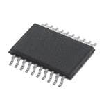
| 描述 | IC ADC 24BIT 2CH W/LNA 20SSOP模数转换器 - ADC 2-Ch 24-Bit ADCs w/ Ultra Low Noise PGIA |
| 产品分类 | |
| 品牌 | Cirrus Logic |
| 产品手册 | |
| 产品图片 |
|
| rohs | 符合RoHS无铅 / 符合限制有害物质指令(RoHS)规范要求 |
| 产品系列 | 数据转换器IC,模数转换器 - ADC,Cirrus Logic CS5532-ASZ- |
| 数据手册 | |
| 产品型号 | CS5532-ASZ |
| 产品目录页面 | |
| 产品种类 | 模数转换器 - ADC |
| 位数 | 24 |
| 供应商器件封装 | 20-SSOP |
| 信噪比 | No |
| 其它名称 | 598-1112-5 |
| 分辨率 | 16 bit |
| 包装 | 管件 |
| 商标 | Cirrus Logic |
| 商标名 | CS5532 |
| 安装类型 | 表面贴装 |
| 安装风格 | SMD/SMT |
| 封装 | Tube |
| 封装/外壳 | 20-SSOP(0.209",5.30mm 宽) |
| 封装/箱体 | SSOP-20 |
| 工作温度 | -40°C ~ 85°C |
| 工作电源电压 | +/- 2.5 V to +/- 5 V |
| 工厂包装数量 | 66 |
| 接口类型 | Serial (3-Wire) |
| 数据接口 | 串行 |
| 最大功率耗散 | 500 mW |
| 最大工作温度 | + 85 C |
| 最小工作温度 | - 40 C |
| 标准包装 | 66 |
| 特性 | PGA |
| 电压参考 | 2.5 V |
| 电压源 | 模拟和数字,双 ± |
| 系列 | CS5531-AS |
| 结构 | Sigma-Delta |
| 转换器数 | 1 |
| 转换器数量 | 1 |
| 转换速率 | 6.25 S/s to 3840 S/s |
| 输入数和类型 | 2 个差分,单极2 个差分,双极 |
| 输入类型 | Differential |
| 通道数量 | 2 Channel |
| 配用 | /product-detail/zh/CDB5532U/598-1159-ND/1245609 |
| 采样率(每秒) | 3.84k |


- 商务部:美国ITC正式对集成电路等产品启动337调查
- 曝三星4nm工艺存在良率问题 高通将骁龙8 Gen1或转产台积电
- 太阳诱电将投资9.5亿元在常州建新厂生产MLCC 预计2023年完工
- 英特尔发布欧洲新工厂建设计划 深化IDM 2.0 战略
- 台积电先进制程称霸业界 有大客户加持明年业绩稳了
- 达到5530亿美元!SIA预计今年全球半导体销售额将创下新高
- 英特尔拟将自动驾驶子公司Mobileye上市 估值或超500亿美元
- 三星加码芯片和SET,合并消费电子和移动部门,撤换高东真等 CEO
- 三星电子宣布重大人事变动 还合并消费电子和移动部门
- 海关总署:前11个月进口集成电路产品价值2.52万亿元 增长14.8%


PDF Datasheet 数据手册内容提取
CS5531/32/33/34-AS 16-bit and 24-bit ADCs with Ultra-low-noise PGIA Features General Description (cid:137)Chopper-stabilized PGIA (Programmable The CS5531/32/33/34 are highly integrated ∆Σ Analog- Gain Instrumentation Amplifier, 1x to 64x) to-Digital Converters (ADCs) which use charge-balance – 12 nV/√Hz @ 0.1 Hz (No 1/f noise) at 64x techniques to achieve 16-bit (CS5531/33) and 24-bit (CS5532/34) performance. The ADCs are optimized for – 1200pA Input Current with Gains >1 measuring low-level unipolar or bipolar signals in weigh (cid:137)Delta-sigma Analog-to-digital Converter scale, process control, scientific, and medical applications. – Linearity Error: 0.0007% FS – Noise Free Resolution: Up to 23 bits To accommodate these applications, the ADCs come as either two-channel (CS5531/32) or four-channel (cid:137)Two- or Four-channel Differential MUX (CS5533/34) devices and include a very low noise chop- (cid:137)Scalable Input Span via Calibration per-stabilized instrumentation amplifier (6 nV/√Hz @ 0.1 Hz) with selectable gains of 1×, 2×, 4×, 8×, 16×, 32×, and – ±5 mV to differential ±2.5V 64×. These ADCs also include a fourth order ∆Σ modu- (cid:137)Scalable V Input: Up to Analog Supply lator followed by a digital filter which provides twenty REF selectable output word rates of 6.25, 7.5, 12.5, 15, 25, 30, (cid:137)Simple Three-wire Serial Interface 50, 60, 100, 120, 200, 240, 400, 480, 800, 960, 1600, 1920, 3200, and 3840 Sps (MCLK=4.9152MHz). – SPI™ and Microwire™ Compatible – Schmitt Trigger on Serial Clock (SCLK) To ease communication between the ADCs and a micro- controller, the converters include a simple three-wire se- (cid:137)R/W Calibration Registers Per Channel rial interface which is SPI and Microwire compatible with (cid:137)Selectable Word Rates: 6.25 to 3,840 Sps a Schmitt-trigger input on the serial clock (SCLK). High dynamic range, programmable output rates, and (cid:137)Selectable 50 or 60 Hz Rejection flexible power supply options makes these ADCs ideal (cid:137)Power Supply Configurations solutions for weigh scale and process control applications. – VA+ = +5 V; VA- = 0 V; VD+ = +3 V to +5 V – VA+ = +2.5 V; VA- = -2.5 V; VD+ = +3 V to +5 V ORDERING INFORMATION – VA+ = +3 V; VA- = -3 V; VD+ = +3 V See page47 VA+ C1 C2 VREF+ VREF- VD+ CS AIN1+ PGIA DIFFERENTIAL AIN1- 13,22,6,44,8,16 4MTHO DOURLDAETRO ∆RΣ PSRINOCG RFIARM FMILATBELRE SERIAL SDI AIN2+ INTERFACE SDO AIN2- MUX SCLK (CS5533/34 AIN3+ SHOWN) AIN3- CLOCK AIN4+ LATCH GENERATOR CALIBRATION SRAM/CONTROL AIN4- LOGIC VA- A0/GUARD A1 OSC1 OSC2 DGND OCT ‘08 Copyright © Cirrus Logic, Inc. 2008 http://www.cirrus.com (All Rights Reserved) DS289F5
CS5531/32/33/34-AS TABLE OF CONTENTS 1. CHARACTERISTICS AND SPECIFICATIONS ..........................................................4 ANALOG CHARACTERISTICS..........................................................................4 TYPICAL RMS NOISE (NV), CS5531/32/33/34.................................................7 TYPICAL NOISE-FREE RESOLUTION(BITS), CS5532/34...............................7 5 V DIGITAL CHARACTERISTICS....................................................................8 3 V DIGITAL CHARACTERISTICS....................................................................8 DYNAMIC CHARACTERISTICS........................................................................9 ABSOLUTE MAXIMUM RATINGS.....................................................................9 SWITCHING CHARACTERISTICS..................................................................10 2. GENERAL DESCRIPTION .......................................................................................12 2.1. Analog Input ....................................................................................................12 2.1.1. Analog Input Span ....................................................................................13 2.1.2. Multiplexed Settling Limitations ............................................................13 2.1.3. Voltage Noise Density Performance .....................................................13 2.1.4. No Offset DAC ......................................................................................14 2.2. Overview of ADC Register Structure and Operating Modes ............................14 2.2.1. System Initialization ..............................................................................15 2.2.2. Serial Port Interface ..............................................................................22 2.2.3. Reading/Writing On-Chip Registers ......................................................23 2.3. Configuration Register .....................................................................................23 2.3.1. Power Consumption .............................................................................23 2.3.2. System Reset Sequence ......................................................................23 2.3.3. Input Short ............................................................................................24 2.3.4. Guard Signal .........................................................................................24 2.3.5. Voltage Reference Select .....................................................................24 2.3.6. Output Latch Pins .................................................................................24 2.3.7. Offset and Gain Select ..........................................................................25 2.3.8. Filter Rate Select ..................................................................................25 2.4. Setting up the CSRs for a Measurement .........................................................27 2.5. Calibration ........................................................................................................30 2.5.1. Calibration Registers ............................................................................30 2.5.2. Performing Calibrations ........................................................................31 2.5.3. Self-calibration ......................................................................................31 2.5.4. System Calibration ................................................................................32 2.5.5. Calibration Tips .....................................................................................32 2.5.6. Limitations in Calibration Range ...........................................................33 2.6. Performing Conversions ..................................................................................33 2.6.1. Single Conversion Mode .......................................................................33 2.6.2. Continuous Conversion Mode ..............................................................34 2.6.3. Examples of Using CSRs to Perform Conversions and Calibrations ....35 2.7. Using Multiple ADCs Synchronously ...............................................................36 2.8. Conversion Output Coding ..............................................................................36 2.9. Digital Filter ......................................................................................................38 2.10. Clock Generator ...............................................................................................39 2.11. Power Supply Arrangements ...........................................................................39 2.12. Getting Started ................................................................................................43 2.13. PCB Layout .....................................................................................................43 3. PIN DESCRIPTIONS ...............................................................................................44 4. SPECIFICATION DEFINITIONS ...............................................................................46 5. ORDERING INFORMATION .....................................................................................47 6. ENVIRONMENTAL, MANUFACTURING, & HANDLING INFORMATION ..............47 7. PACKAGE DRAWINGS ...........................................................................................48 2 DS289F5
CS5531/32/33/34-AS LIST OF FIGURES Figure 1. SDI Write Timing (Not to Scale)...............................................................................11 Figure 2. SDO Read Timing (Not to Scale).............................................................................11 Figure 3. Multiplexer Configuration.........................................................................................12 Figure 4. Input models for AIN+ and AIN- pins.......................................................................13 Figure 5. Measured Voltage Noise Density.............................................................................13 Figure 6. CS5531/32/33/34 Register Diagram........................................................................14 Figure 7. Command and Data Word Timing...........................................................................22 Figure 8. Guard Signal Shielding Scheme..............................................................................24 Figure 9. Input Reference Model when VRS = 1....................................................................25 Figure 10. Input Reference Model when VRS = 0..................................................................25 Figure 11. Self-calibration of Offset.........................................................................................32 Figure 12. Self-calibration of Gain...........................................................................................32 Figure 13. System Calibration of Offset..................................................................................32 Figure 14. System Calibration of Gain....................................................................................32 Figure 15. Synchronizing Multiple ADCs.................................................................................36 Figure 16. Digital Filter Response (Word Rate = 60 Sps).......................................................38 Figure 17. 120 Sps Filter Magnitude Plot to 120 Hz...............................................................38 Figure 18. 120 Sps Filter Phase Plot to 120 Hz......................................................................38 Figure 19. Z-Transforms of Digital Filters................................................................................38 Figure 20. On-chip Oscillator Model........................................................................................39 Figure 21. CS5532 Configured with a Single +5 V Supply.....................................................40 Figure 22. CS5532 Configured with ±2.5 V Analog Supplies..................................................41 Figure 23. CS5532 Configured with ±3 V Analog Supplies.....................................................41 Figure 24. CS5532 Configured for Thermocouple Measurement...........................................42 Figure 25. Bridge with Series Resistors..................................................................................42 LIST OF TABLES Table 1. Conversion Timing – Single Mode............................................................................34 Table 2. Conversion Timing – Continuous Mode....................................................................34 Table 3. Command Byte Pointer.............................................................................................35 Table 4. Output Coding for 16-bit CS5531 and CS5533.........................................................36 Table 5. Output Coding for 24-bit CS5532 and CS5534.........................................................37 DS289F5 3
CS5531/32/33/34-AS 1. CHARACTERISTICS AND SPECIFICATIONS ANALOG CHARACTERISTICS (VA+, VD+ = 5 V ±5%; VREF+ = 5 V; VA-, VREF-, DGND = 0 V; MCLK = 4.9152 MHz; OWR (Output Word Rate) = 60 Sps; Bipolar Mode; Gain = 32) (See Notes 1 and 2.) CS5531/CS5533 Parameter Min Typ Max Unit Accuracy Linearity Error - ±0.0015 ±0.003 %FS No Missing Codes 16 - - Bits Bipolar Offset - ±1 ±2 LSB 16 Unipolar Offset - ±2 ±4 LSB 16 Offset Drift (Notes 3 and 4) - 10 - nV/°C Bipolar Full-scale Error - ±8 ±31 ppm Unipolar Full-scale Error - ±16 ±62 ppm Full-scale Drift (Note 4) - 2 - ppm/°C CS5532/CS5534 Parameter Min Typ Max Unit Accuracy Linearity Error - ±0.0015 ±0.003 %FS No Missing Codes 24 - - Bits Bipolar Offset - ±16 ±32 LSB 24 Unipolar Offset - ±32 ±64 LSB 24 Offset Drift (Notes 3 and 4) - 10 - nV/°C Bipolar Full-scale Error - ±8 ±31 ppm Unipolar Full-scale Error - ±16 ±62 ppm Full-scale Drift (Note 4) - 2 - ppm/°C Notes: 1. Applies after system calibration at any temperature within -40 °C ~ +85 °C. 2. Specifications guaranteed by design, characterization, and/or test. LSB is 16 bits for the CS5531/33 and LSB is 24 bits for the CS5532/34. 3. This specification applies to the device only and does not include any effects by external parasitic thermocouples. 4. Drift over specified temperature range after calibration at power-up at 25 °C. 4 DS289F5
CS5531/32/33/34-AS ANALOG CHARACTERISTICS (Continued) (See Notes 1 and 2.) Parameter Min Typ Max Unit Analog Input Common Mode + Signal on AIN+ or AIN-Bipolar/Unipolar Mode Gain = 1 VA- - VA+ V Gain = 2, 4, 8, 16, 32, 64 (Note 5) VA- + 0.7 - VA+ - 1.7 V CVF Current on AIN+ or AIN- Gain = 1 (Note 6, 7) - 50 - nA Gain = 2, 4, 8, 16, 32, 64 - 1200 - pA Input Current Noise Gain = 1 - 200 - pA/√Hz Gain = 2, 4, 8, 16, 32, 64 - 1 - pA/√Hz Input Leakage for Mux when Off (at 25 °C) - 10 - pA Off-channel Mux Isolation - 120 - dB Open Circuit Detect Current 100 300 - nA Common Mode Rejection dc, Gain = 1 - 90 - dB dc, Gain = 64 - 130 - dB 50, 60 Hz - 120 - dB Input Capacitance - 60 - pF Guard Drive Output - 20 - µA Voltage Reference Input Range (VREF+) - (VREF-) 1 2.5 (VA+)-(VA-) V CVF Current (Note 6, 7) - 50 - nA Common Mode Rejection dc - 120 - dB 50, 60 Hz - 120 - dB Input Capacitance 11 - 22 pF System Calibration Specifications Full-scale Calibration Range Bipolar/Unipolar Mode 3 - 110 %FS Offset Calibration Range Bipolar Mode -100 - 100 %FS Offset Calibration Range Unipolar Mode -90 - 90 %FS Notes: 5. The voltage on the analog inputs is amplified by the PGIA, and becomes V ± Gain*(AIN+ - AIN-)/2 at CM the differential outputs of the amplifier. In addition to the input common mode + signal requirements for the analog input pins, the differential outputs of the amplifier must remain between (VA- + 0.1 V) and (VA+ - 0.1 V) to avoid saturation of the output stage. 6. See the section of the data sheet which discusses input models. 7. Input current on AIN+ or AIN- (with Gain=1), or VREF+ or VREF- may increase to 250nA if operated within 50mV of VA+ or VA-. This is due to the rough charge buffer being saturated under these conditions. DS289F5 5
CS5531/32/33/34-AS ANALOG CHARACTERISTICS (Continued) (See Notes 1 and 2.) Parameter Min Typ Max Unit Power Supplies DC Power Supply Currents (Normal Mode) I I - 6 8 mA A+, A- I - 0.6 1 mA D+ Power Consumption Normal Mode (Notes 8 and 9) - 35 45 mW Standby - 5 - mW Sleep - 500 - µW Power Supply Rejection (Note 10) dc Positive Supplies - 115 - dB dc Negative Supply - 115 - dB 8. All outputs unloaded. All input CMOS levels. 9. Power is specified when the instrumentation amplifier (Gain ≥ 2) is on. Analog supply current is reduced by approximately 1/2 when the instrumentation amplifier is off (Gain = 1). 10. Tested with 100 mV change on VA+ or VA-. 6 DS289F5
CS5531/32/33/34-AS TYPICAL RMS NOISE (nV), CS5531/32/33/34 (See notes 11, 12 and 13) Output Word -3 dB Filter Instrumentation Amplifier Gain Rate (Sps) Frequency (Hz) x64 x32 x16 x8 x4 x2 x1 7.5 1.94 17 17 19 26 42 79 155 15 3.88 24 25 27 36 59 111 218 30 7.75 34 35 39 51 84 157 308 60 15.5 48 49 54 72 118 222 436 120 31 68 70 77 102 167 314 616 240 62 115 160 276 527 1040 2070 4150 480 122 163 230 392 748 1480 2950 5890 960 230 229 321 554 1060 2090 4170 8340 1,920 390 344 523 946 1840 3650 7290 14600 3,840 780 1390 2710 5390 10800 21500 43000 86100 Notes:11. Wideband noise aliased into the baseband. Referred to the input. Typical values shown for 25 °C. 12. For peak-to-peak noise multiply by 6.6 for all ranges and output rates. 13. Word rates and -3dB points with FRS = 0. When FRS = 1, word rates and -3dB points scale by 5/6. TYPICAL NOISE-FREE RESOLUTION(BITS), CS5532/34 (See Notes 14 and 15) Output Word -3 dB Filter Instrumentation Amplifier Gain Rate (Sps) Frequency (Hz) x64 x32 x16 x8 x4 x2 x1 7.5 1.94 19 20 21 22 22 22 22 15 3.88 19 20 21 21 21 22 22 30 7.75 18 19 20 21 21 21 21 60 15.5 18 19 20 20 20 21 21 120 31 17 18 19 20 20 20 20 240 62 16 17 17 17 17 17 17 480 122 16 17 17 17 17 17 17 960 230 15 16 16 16 16 16 16 1,920 390 15 15 15 15 15 15 15 3,840 780 13 13 13 13 13 13 13 14. Noise-free resolution listed is for bipolar operation, and is calculated as LOG((Input Span)/(6.6xRMS Noise))/LOG(2) rounded to the nearest bit. For unipolar operation, the input span is 1/2 as large, so one bit is lost. The input span is calculated in the analog input span section of the data sheet. The noise-free resolution table is computed with a value of 1.0 in the gain register. Values other than 1.0 will scale the noise, and change the noise-free resolution accordingly. 15. “Noise-free resolution” is not the same as “effective resolution”. Effective resolution is based on the RMS noise value, while noise-free resolution is based on a peak-to-peak noise value specified as 6.6 times the RMS noise value. Effective resolution is calculated as LOG((Input Span)/(RMS Noise))/LOG(2). Specifications are subject to change without notice. DS289F5 7
CS5531/32/33/34-AS 5 V DIGITAL CHARACTERISTICS (VA+, VD+ = 5 V ±5%; VA-, DGND = 0 V; See Notes 2 and 16.) Parameter Symbol Min Typ Max Unit High-level Input Voltage All Pins Except SCLK V 0.6 VD+ - VD+ V IH SCLK (VD+) - 0.45 - VD+ Low-level Input Voltage All Pins Except SCLK V 0.0 - 0.8 V IL SCLK 0.0 0.6 High-level Output Voltage A0 and A1, I = -1.0 mA V (VA+) - 1.0 - - V out OH SDO, I = -5.0 mA (VD+) - 1.0 out Low-level Output Voltage A0 and A1, I = 1.0 mA V - - (VA-) + 0.4 V out OL SDO, I = 5.0 mA 0.4 out Input Leakage Current I - ±1 ±10 µA in SDO Tri-state Leakage Current I - - ±10 µA OZ Digital Output Pin Capacitance C - 9 - pF out 3 V DIGITAL CHARACTERISTICS (T = 25 °C; VA+ = 5V ±5%; VD+ = 3.0V±10%; VA-, DGND = 0V; A See Notes 2 and 16.) Parameter Symbol Min Typ Max Unit High-level Input Voltage All Pins Except SCLK V 0.6 VD+ - VD+ V IH SCLK (VD+) - 0.45 VD+ Low-level Input Voltage All Pins Except SCLK V 0.0 - 0.8 V IL SCLK 0.0 0.6 High-level Output Voltage A0 and A1, I = -1.0 mA V (VA+) - 1.0 - - V out OH SDO, I = -5.0 mA (VD+) - 1.0 out Low-level Output Voltage A0 and A1, I = 1.0 mA V - - (VA-) + 0.4 V out OL SDO, I = 5.0 mA 0.4 out Input Leakage Current I - ±1 ±10 µA in SDO Tri-state Leakage Current I - - ±10 µA OZ Digital Output Pin Capacitance C - 9 - pF out 16. All measurements performed under static conditions. 8 DS289F5
CS5531/32/33/34-AS DYNAMIC CHARACTERISTICS Parameter Symbol Ratio Unit Modulator Sampling Rate f MCLK/16 Sps s Filter Settling Time to 1/2 LSB (Full-scale Step Input) Single Conversion mode (Notes 17, 18, and 19) t 1/OWR s s SC Continuous Conversion mode, OWR < 3200 Sps t 5/OWR + 3/OWR s s sinc5 Continuous Conversion mode, OWR ≥ 3200 Sps s t 5/OWR s 17. The ADCs use a Sinc5 filter for the 3200 Sps and 3840 Sps output word rate (OWR) and a Sinc5 filter followed by a Sinc3 filter for the other OWRs. OWR refers to the 3200 Sps (FRS = 1) or 3840 Sps sinc5 (FRS = 0) word rate associated with the Sinc5 filter. 18. The single conversion mode only outputs fully settled conversions. See Table 1 for more details about single conversion mode timing. OWR is used here to designate the different conversion time SC associated with single conversions. 19. The continuous conversion mode outputs every conversion. This means that the filter’s settling time with a full-scale step input in the continuous conversion mode is dictated by the OWR. ABSOLUTE MAXIMUM RATINGS (DGND = 0 V; See Note 20.) Parameter Symbol Min Typ Max Unit DC Power Supplies (Notes 21 and 22) Positive Digital VD+ -0.3 - +6.0 V Positive Analog VA+ -0.3 - +6.0 V Negative Analog VA- +0.3 - -3.75 V Input Current, Any Pin Except Supplies (Notes 23 and 24) I - - ±10 mA IN Output Current I - - ±25 mA OUT Power Dissipation (Note 25) PDN - - 500 mW Analog Input Voltage VREF pins V (VA-) -0.3 - (VA+) + 0.3 V INR AIN Pins V (VA-) -0.3 - (VA+) + 0.3 V INA Digital Input Voltage V -0.3 - (VD+) + 0.3 V IND Ambient Operating Temperature T -40 - 85 °C A Storage Temperature T -65 - 150 °C stg Notes:20. All voltages with respect to ground. 21. VA+ and VA- must satisfy {(VA+) - (VA-)} ≤ +6.6 V. 22. VD+ and VA- must satisfy {(VD+) - (VA-)} ≤ +7.5 V. 23. Applies to all pins including continuous overvoltage conditions at the analog input (AIN) pins. 24. Transient current of up to 100 mA will not cause SCR latch-up. Maximum input current for a power supply pin is ±50 mA. 25. Total power dissipation, including all input currents and output currents. WARNING:Operation at or beyond these limits may result in permanent damage to the device. Normal operation is not guaranteed at these extremes. DS289F5 9
CS5531/32/33/34-AS SWITCHING CHARACTERISTICS (VA+ = 2.5 V or 5 V ±5%; VA- = -2.5V±5% or 0 V; VD+ = 3.0 V ±10% or 5 V ±5%;DGND = 0 V; Levels: Logic 0 = 0 V, Logic 1 = VD+; C = 50 pF; See Figures 1 and 2.) L Parameter Symbol Min Typ Max Unit Master Clock Frequency (Note 26) MCLK External Clock or Crystal Oscillator 1 4.9152 5 MHz Master Clock Duty Cycle 40 - 60 % Rise Times (Note 27) t rise Any Digital Input Except SCLK - - 1.0 µs SCLK - - 100 µs Any Digital Output - 50 - ns Fall Times (Note 27) t fall Any Digital Input Except SCLK - - 1.0 µs SCLK - - 100 µs Any Digital Output - 50 - ns Start-up Oscillator Start-up Time XTAL = 4.9152 MHz (Note 28) t - 20 - ms ost Serial Port Timing Serial Clock Frequency SCLK 0 - 2 MHz Serial Clock Pulse Width High t 250 - - ns 1 Pulse Width Low t 250 - - ns 2 SDI Write Timing CS Enable to Valid Latch Clock t 50 - - ns 3 Data Set-up Time prior to SCLK rising t 50 - - ns 4 Data Hold Time After SCLK Rising t 100 - - ns 5 SCLK Falling Prior to CS Disable t 100 - - ns 6 SDO Read Timing CS to Data Valid t - - 150 ns 7 SCLK Falling to New Data Bit t - - 150 ns 8 CS Rising to SDO Hi-Z t - - 150 ns 9 Notes:26. Device parameters are specified with a 4.9152 MHz clock. 27. Specified using 10% and 90% points on waveform of interest. Output loaded with 50pF. 28. Oscillator start-up time varies with crystal parameters. This specification does not apply when using an external clock source. 10 DS289F5
CS5531/32/33/34-AS CS t3 SDI MSB MSB-1 LSB t4 t5 t1 t6 SCLK t2 Figure 1. SDI Write Timing (Not to Scale) CS t7 t9 SDO MSB MSB-1 LSB t8 t2 SCLK t1 Figure 2. SDO Read Timing (Not to Scale) DS289F5 11
CS5531/32/33/34-AS 2. GENERAL DESCRIPTION The CS5531/32/33/34 are highly integrated ∆Σ An- crowire compatible with a Schmitt-trigger input on alog-to-Digital Converters (ADCs) which use the serial clock (SCLK). charge-balance techniques to achieve 16-bit 2.1. Analog Input (CS5531/33) and 24-bit (CS5532/34) performance. Figure 3 illustrates a block diagram of the The ADCs are optimized for measuring low-level CS5531/32/33/34. The front end consists of a multi- unipolar or bipolar signals in weigh scale, process plexer, a unity gain coarse/fine charge input buffer, control, scientific, and medical applications. and a programmable gain chopper-stabilized instru- To accommodate these applications, the ADCs mentation amplifier. The unity gain buffer is activat- come as either two-channel (CS5531/32) or four- ed any time conversions are performed with a gain channel (CS5533/34) devices and include a very- of one and the instrumentation amplifier is activated low-noise, chopper-stabilized, programmable-gain any time conversions are performed with gain set- instrumentation amplifier (PGIA, 6 nV/√Hz @ 0.1 tings greater than one. Hz) with selectable gains of 1×, 2×, 4×, 8×, 16×, The unity gain buffer is designed to accommodate 32×, and 64×. These ADCs also include a fourth or- rail to rail input signals. The common-mode plus der ∆Σ modulator followed by a digital filter which signal range for the unity gain buffer amplifier is provides twenty selectable output word rates of 6.25, VA- to VA+. Typical CVF (sampling) current for 7.5, 12.5, 15, 25, 30, 50, 60, 100, 120, 200, 240, 400, the unity gain buffer amplifier is about 50nA 480, 800, 960, 1600, 1920, 3200, and 3840 Samples (MCLK = 4.9152 MHz, see Figure 4). per second (MCLK = 4.9152 MHz). The instrumentation amplifier is chopper stabilized To ease communication between the ADCs and a and operates with a chop clock frequency of microcontroller, the converters include a simple MCLK/128. The CVF (sampling) current into the three-wire serial interface which is SPI and Mi- VREF+ VREF- AIN2+ CS5531/32 IN+ X1 X1 AIN2- M X1 AIN1+ U X1 AIN1- X IN- 1000 Ω Differential IN+ XGAIN 22 nF C1 PIN 4 t h ∆OΣrder DSiginitca5l ProgrSaimncm3able Serial AIN4+ C2 PIN Modulator Filter Digital Filter Port AIN4- CS5533/34 IN- 1000 Ω IN+ * M X1 X1 * U * X IN- AIN1+ GAIN is the gain setting of the PGIA (i.e. 2, 4, 8, 16, 32, 64) AIN1- Figure 3. Multiplexer Configuration 12 DS289F5
CS5531/32/33/34-AS instrumentation amplifier is typically 1200 pA Select bit, and must be set according to the differen- over -40°C to +85°C (MCLK=4.9152 MHz). tial voltage applied to the VREF+ and VREF- pins The common-mode plus signal range of the instru- on the part. See section 2.3.5 for more details. mentation amplifier is (VA-) + 0.7 V to (VA+) - After reset, the unity gain buffer is engaged. With a 1.7 V. 2.5V reference this would make the full-scale input Figure 4 illustrates the input models for the ampli- range default to 2.5 V. By activating the instrumen- fiers. The dynamic input current for each of the tation amplifier (i.e. a gain setting other than 1) and pins can be determined from the models shown. using a gain setting of 32, the full-scale input range can quickly be set to 2.5/32 or about 78 mV. Note that these input ranges assume the calibration regis- ters are set to their default values (i.e. Gain = 1.0 and Gain=2,4,8,16,32,64 Offset = 0.0). AIN C=3.9pF 2.1.2. Multiplexed Settling Limitations V ≤8mV The settling performance of the CS5531/32/33/34 os in=fVosC in multiplexed applications is affected by the sin- MCLK f= 128 gle-pole, low-pass filter which follows the instru- mentation amplifier (see Figure 3). To achieve data Gain=1 φ1Fine sheet settling and linearity specifications, it is rec- ommended that a 22 nF C0G capacitor be used. φ1Coarse AIN Capacitors as low as 10 nF or X7R type capacitors can also be used with some minor increase in dis- V ≤12mV C=14pF os tortion for AC signals. i =fV C n os MCLK 2.1.3. Voltage Noise Density Performance f= 16 Figure 5 illustrates the measured voltage noise density versus frequency from 0.025 Hz to 10 Hz Figure 4. Input models for AIN+ and AIN- pins of a CS5532-AS. The device was powered with ±2.5 V supplies, using 30 Sps OWR, the 64x gain range, bipolar mode, and with the input short bit Note: The C=3.9pF and C = 14pF capacitors are enabled. for input current modeling only. For physical input capacitance see ‘Input Capacitance’ 1000 specification under Analog Characteristics. 2.1.1. Analog Input Span 100 The full-scale input signal that the converter can digitize is a function of the gain setting and the ref- 10 erence voltage connected between the VREF+ and VREF- pins. The full-scale input span of the con- 1 0.025 0.10 1.00 10.00 verter is [(VREF+) - (VREF-)]/(GxA), where G is Frequency(Hz) the gain of the amplifier and A is 2 for VRS = 0, or Figure 5. Measured Voltage Noise Density, 64x A is 1 for VRS = 1. VRS is the Voltage Reference DS289F5 13
CS5531/32/33/34-AS 2.1.4. No Offset DAC converters with four channels have four offset and An offset DAC was not included in the CS553X four gain calibration registers. These registers hold family because the high dynamic range of the con- calibration results. The contents of these registers verter eliminates the need for one. The offset regis- can be read or written by the user. This allows cal- ter can be manipulated by the user to mimic the ibration data to be off-loaded into an external EE- function of a DAC if desired. PROM. The user can also manipulate the contents of these registers to modify the offset or the gain 2.2. Overview of ADC Register Structure slope of the converter. and Operating Modes The converters include a 32-bit configuration reg- The CS5531/32/33/34 ADCs have an on-chip con- ister which is used for setting options such as the troller, which includes a number of user-accessible power down modes, resetting the converter, short- registers. The registers are used to hold offset and ing the analog inputs, and enabling diagnostic test gain calibration results, configure the chip's operat- bits like the guard signal. ing modes, hold conversion instructions, and to store conversion data words. Figure 6 depicts a A group of registers, called Channel Setup Regis- block diagram of the on-chip controller’s internal ters, are used to hold pre-loaded conversion in- registers. structions. Each channel setup register is 32 bits long, and holds two 16-bit conversion instructions Each of the converters has 32-bit registers to func- referred to as Setups. Upon power up, these regis- tion as offset and gain calibration registers for each ters can be initialized by the system microcontrol- channel. The converters with two channels have ler with conversion instructions. The user can then two offset and two gain calibration registers, the OffsetRegisters(4x32) GainRegisters(4x32) RCeghaisntenresl(S4extu3p2) CRoengvisetresrio(n1Dxa3t2a) Offset1(1x32) Gain1(1x32) Setup1 Setup2 Data(1x32) (1x16) (1x16) Offset2 (1x32) Gain2(1x32) Setup3 Setup4 (1x16) (1x16) y nl O d Offset3 (1x32) Gain3(1x32) Setup5 Setup6 ea (1x16) (1x16) R Setup7 Setup8 Offset4 (1x32) Gain4(1x32) (1x16) (1x16) CS Serial SDI Interface SDO SCLK y ConfigurationRegister(1x32) nl O e Writ PowerSaveSelect ChannelSelect ResetSystem Gain Command InputShort WordRate Register(1×8) GuardSignal Unipolar/Bipolar VoltageReferenceSelect OutputLatch OutputLatch DelayTime OutputLatchSelect OpenCircuitDetect Offset/Gain Select Offset/Gain Pointer Filter Rate Select Figure 6. CS5531/32/33/34 Register Diagram 14 DS289F5
CS5531/32/33/34-AS instruct the converter to perform single or multiple This sequence resets the serial port to the command conversions or calibrations with the converter in mode and is accomplished by transmitting at least the mode defined by one of these Setups. 15 SYNC1 command bytes (0xFF hexadecimal), followed by one SYNC0 command (0xFE hexa- Using the single conversion mode, an 8-bit com- decimal). Note that this sequence can be initiated at mand word can be written into the serial port. The anytime to reinitialize the serial port. To complete command includes pointer bits which ‘point’ to a the system initialization sequence, the user must 16-bit command in one of the Channel Setup Reg- also perform a system reset sequence which is as isters which is to be executed. The 16-bit Setups follows: Write a logic 1 into the RS bit of the con- can be programmed to perform a conversion on any figuration register. This will reset the calibration of the input channels of the converter. More than registers and other logic (but not the serial port). A one of the 16-bit Setups can be used for the same valid reset will set the RV bit in the configuration analog input channel. This allows the user to con- register to a logic 1. After writing the RS bit to a vert on the same signal with either a different con- logic 1, wait 20 microseconds, then write the RS bit version speed, a different gain range, or any of the back to logic 0. While this involves writing an en- other options available in the channel setup regis- tire word into the configuration register, the RV bit ters. Alternately, the user can set up the registers to is a read only bit, therefore a write to the configu- perform different conversion conditions on each of ration register will not overwrite the RV bit. After the input channels. clearing the RS bit back to logic 0, read the config- The ADCs also include continuous conversion ca- uration register to check the state of the RV bit as pability. The ADCs can be instructed to continu- this indicates that a valid reset occurred. Reading ously convert, referencing one 16-bit command the configuration register clears the RV bit back to Setup. In the continuous conversions mode, the logic 0. conversion data words are loaded into a shift regis- Completing the reset cycle initializes the on-chip ter. The converter issues a flag on the SDO pin registers to the following states: when a conversion cycle is completed so the user can read the register, if need be. See the section on Configuration Register: 00000000(H) Performing Conversions for more details. Offset Registers: 00000000(H) The following pages document how to initialize the Gain Registers: 01000000(H) converter, perform offset and gain calibrations, and Channel Setup Registers: 00000000(H) how to configure the converter for the various con- version modes. Each of the bits of the configuration Note: Previous datasheets stated that the RS bit register and of the Channel Setup Registers is de- would clear itself back to logic 0 and therefore scribed. A list of examples follows the description the user was not required to write the RS bit back to logic 0. The current data sheet section. Also the Command Register Quick Refer- instruction that requires the user to write into ence can be used to decode all valid commands (the the configuration register to clear the RS bit first 8-bits into the serial port). has been added to insure that the RS bit is cleared. Characterization across multiple lots 2.2.1. System Initialization of silicon has indicated some chips do not automatically reset the RS bit to logic 0 in the The CS5531/32/33/34 provide no power-on-reset configuration register, although the reset function. To initialize the ADCs, the user must per- function is completed. This occurs only on form a software reset by resetting the ADC’s serial small number of chips when the VA- supply is port with the Serial Port Initialization sequence. negative with respect to DGND. This has not DS289F5 15
CS5531/32/33/34-AS caused an operational issue for customers reset cycle. After a system initialization or reset, because their start-up sequence includes the on-chip controller is initialized into command writing a word (with RS=0) into the mode where it waits for a valid command (the first configuration register after performing a reset. The change in the reset sequence to 8-bits written into the serial port are shifted into the include writing the RS bit back to 0 insures command register). Once a valid command is re- the clearing of the RS bit in the event that a ceived and decoded, the byte instructs the converter user does not write into the configuration register after the RS bit has been set. to either acquire data from or transfer data to an in- ternal register(s), or perform a conversion or a cal- The RV bit in the Configuration Register is set to ibration. The Command Register Descriptions indicate a valid reset has occurred. The RS bit section can be used to decode all valid commands. should be written back to logic “0” to complete the 16 DS289F5
CS5531/32/33/34-AS 2.2.2. Command Register Quick Reference D7(MSB) D6 D5 D4 D3 D2 D1 D0 0 ARA CS1 CS0 R/W RSB2 RSB1 RSB0 BIT NAME VALUE FUNCTION D7 Command Bit, C 0 Must be logic 0 for these commands. 1 These commands are invalid if this bit is logic 1. D6 Access Registers as 0 Ignore this function. Arrays, ARA 1 Access the respective registers, offset, gain, or channel-setup, as an array of regis- ters. The particular registers accessed are determined by the RS bits. The registers are accessed MSB first with physical channel 0 accessed first followed by physical channel 1 next and so forth. D5-D4 Channel Select Bits, 00 CS1-CS0 provide the address of one of the two (four for CS5533/34) physical input CS1-CS0 01 channels. These bits are also used to access the calibration registers associated 10 with the respective physical input channel. Note that these bits are ignored when 11 reading data register. D3 Read/Write, R/W 0 Write to selected register. 1 Read from selected register. D2-D0 Register Select Bit, 000 Reserved RSB3-RSB0 001 Offset Register 010 Gain Register 011 Configuration Register 101 Channel-Setup Registers 110 Reserved 111 Reserved D7(MSB) D6 D5 D4 D3 D2 D1 D0 1 MC CSRP2 CSRP1 CSRP0 CC2 CC1 CC0 BIT NAME VALUE FUNCTION D7 Command Bit, C 0 These commands are invalid if this bit is logic 0. 1 Must be logic 1 for these commands. D6 Multiple Conver- 0 Perform fully settled single conversions. sions, MC 1 Perform conversions continuously. D5-D3 Channel-Setup Reg- 000 These bits are used as pointers to the Channel-Setup registers. Either a single con- ister Pointer Bits, ... version or continuous conversions are performed on the channel setup register CSRP 111 pointed to by these bits. D2-D0 Conversion/Calibra- 000 Normal Conversion tion Bits, CC2-CC0 001 Self-Offset Calibration 010 Self-Gain Calibration 011 Reserved 100 Reserved 101 System-Offset Calibration 110 System-Gain Calibration 111 Reserved DS289F5 17
CS5531/32/33/34-AS 2.2.3. Command Register Descriptions READ/WRITE ALL OFFSET CALIBRATION REGISTERS D7(MSB) D6 D5 D4 D3 D2 D1 D0 0 1 0 0 R/W 0 0 1 Function: These commands are used to access the offset registers as arrays. R/W (Read/Write) 0 Write to selected registers. 1 Read from selected registers. READ/WRITE ALL GAIN CALIBRATION REGISTERS D7(MSB) D6 D5 D4 D3 D2 D1 D0 0 1 0 0 R/W 0 1 0 Function: These commands are used to access the gain registers as arrays. R/W (Read/Write) 0 Write to selected registers. 1 Read from selected registers. READ/WRITE ALL CHANNEL-SETUP REGISTERS D7(MSB) D6 D5 D4 D3 D2 D1 D0 0 1 0 0 R/W 1 0 1 Function: These commands are used to access the channel-setup registers as arrays. R/W (Read/Write) 0 Write to selected registers. 1 Read from selected registers. READ/WRITE INDIVIDUAL OFFSET REGISTER D7(MSB) D6 D5 D4 D3 D2 D1 D0 0 0 CS1 CS0 R/W 0 0 1 Function: These commands are used to access each offset register separately. CS1 - CS0 decode the registers accessed. R/W (Read/Write) 0 Write to selected register. 1 Read from selected register. CS[1:0] (Channel Select Bits) 00 Offset Register 1 (All devices) 01 Offset Register 2 (All devices) 10 Offset Register 3 (CS5533/34 only) 11 Offset Register 4 (CS5533/34 only) 18 DS289F5
CS5531/32/33/34-AS READ/WRITE INDIVIDUAL GAIN REGISTER D7(MSB) D6 D5 D4 D3 D2 D1 D0 0 0 CS1 CS0 R/W 0 1 0 Function: These commands are used to access each gain register separately. CS1 - CS0 decode the reg- isters accessed. R/W (Read/Write) 0 Write to selected register. 1 Read from selected register. CS[1:0] (Channel Select Bits) 00 Gain Register 1 (All devices) 01 Gain Register 2 (All devices) 10 Gain Register 3 (CS5533/34 only) 11 Gain Register 4 (CS5533/34 only) READ/WRITE INDIVIDUAL CHANNEL-SETUP REGISTER D7(MSB) D6 D5 D4 D3 D2 D1 D0 0 0 CS1 CS0 R/W 1 0 1 Function: These commands are used to access each channel-setup register separately. CS1 - CS0 de- code the registers accessed. R/W (Read/Write) 0 Write to selected register. 1 Read from selected register. CS[1:0] (Channel Select Bits) 00 Channel-Setup Register 1 (All devices) 01 Channel-Setup Register 2 (All devices) 10 Channel-Setup Register 3 (All devices) 11 Channel-Setup Register 4 (All devices) READ/WRITE CONFIGURATION REGISTER D7(MSB) D6 D5 D4 D3 D2 D1 D0 0 0 0 0 R/W 0 1 1 Function: These commands are used to read from or write to the configuration register. R/W (Read/Write) 0 Write to selected register. 1 Read from selected register. DS289F5 19
CS5531/32/33/34-AS PERFORM CONVERSION D7(MSB) D6 D5 D4 D3 D2 D1 D0 1 MC CSRP2 CSRP1 CSRP0 0 0 0 Function: These commands instruct the ADC to perform either a single, fully-settled conversion or con- tinuous conversions on the physical input channel pointed to by the pointer bits (CSRP2 - CRSP0) in the channel-setup register. MC (Multiple Conversions) 0 Perform a single conversion. 1 Perform continuous conversions. CSRP [2:0] (Channel Setup Register Pointer Bits) 000 Setup 1 (All devices) 001 Setup 2 (All devices) 010 Setup 3 (All devices) 011 Setup 4 (All devices) 100 Setup 5 (All devices) 101 Setup 6 (All devices) 110 Setup 7 (All devices) 111 Setup 8 (All devices) 20 DS289F5
CS5531/32/33/34-AS PERFORM CALIBRATION D7(MSB) D6 D5 D4 D3 D2 D1 D0 1 0 CSRP2 CSRP1 CSRP0 CC2 CC1 CC0 Function: These commands instruct the ADC to perform a calibration on the physical input channel se- lected by the setup register which is chosen by the command byte pointer bits (CSRP2 - CSRP0). CSRP [2:0] (Channel Setup Register Pointer Bits) 000 Setup 1 (All devices) 001 Setup 2 (All devices) 010 Setup 3 (All devices) 011 Setup 4 (All devices) 100 Setup 5 (All devices) 101 Setup 6 (All devices) 110 Setup 7 (All devices) 111 Setup 8 (All devices) CC [2:0] (Calibration Control Bits) 000 Reserved 001 Self-Offset Calibration 010 Self-Gain Calibration 011 Reserved 100 Reserved 101 System-Offset Calibration 110 System-Gain Calibration 111 Reserved SYNC1 D7(MSB) D6 D5 D4 D3 D2 D1 D0 1 1 1 1 1 1 1 1 Function: Part of the serial port re-initialization sequence. SYNC0 D7(MSB) D6 D5 D4 D3 D2 D1 D0 1 1 1 1 1 1 1 0 Function: End of the serial port re-initialization sequence. NULL D7(MSB) D6 D5 D4 D3 D2 D1 D0 0 0 0 0 0 0 0 0 Function: This command is used to clear a port flag and keep the converter in the continuous conversion mode. DS289F5 21
CS5531/32/33/34-AS 2.2.4. Serial Port Interface SCLK, Serial Clock, is the serial bit-clock which The CS5531/32/33/34’s serial interface consists of controls the shifting of data to or from the ADC’s four control lines: CS, SDI, SDO, SCLK. Figure 7 serial port. The CS pin must be held low (logic 0) details the command and data word timing. before SCLK transitions can be recognized by the port logic. To accommodate optoisolators SCLK is CS, Chip Select, is the control line which enables designed with a Schmitt-trigger input to allow an access to the serial port. If the CS pin is tied low, optoisolator with slower rise and fall times to di- the port can function as a three-wire interface. rectly drive the pin. Additionally, SDO is capable SDI, Serial Data In, is the data signal used to trans- of sinking or sourcing up to 5 mA to directly drive fer data to the converters. an optoisolator LED. SDO will have less than a 400 SDO, Serial Data Out, is the data signal used to mV loss in the drive voltage when sinking or sourc- transfer output data from the converters. The SDO ing 5mA. output will be held at high impedance any time CS is at logic 1. CS SCLK SDI MSB LSB CommandTime DataTime32SCLKs 8SCLKs WriteCycle CS SCLK SDI CommandTime 8SCLKs SDO MSB LSB DataTime32SCLKs ReadCycle CS SCLK SDI CommandTime td* MCLK/OWR ClockCycles 8SCLKs SDO 8SCLKsClearSDOFlag MSB LSB DataTime32SCLKs DataConversionCycle * td is the time it takes the ADC to perform a conversion. See the Single Conversion and Continuous Conversion sections of the data sheet for more details about conversion timing. Figure 7. Command and Data Word Timing 22 DS289F5
CS5531/32/33/34-AS 2.2.5. Reading/Writing On-Chip Registers 2.3.1. Power Consumption The CS5531/32/33/34’s offset, gain, configuration, The CS5531/32/33/34 accommodate three power and channel-setup registers are readable and writ- consumption modes: normal, standby, and sleep. able while the conversion data register is read only. The default mode, “normal mode”, is entered after power is applied. In this mode, the As shown in Figure 7, to write to a particular regis- CS5531/32/33/34 devices typically consume ter the user must transmit the appropriate write 35mW. The other two modes are referred to as the command and then follow that command by 32 bits power-save modes. They power down most of the of data. For example, to write 0x80000000 (hexa- analog portion of the chip and stop filter convolu- decimal) to physical channel one’s gain register, tions. The power-save modes are entered whenever the user would first transmit the command byte the power-down (PDW) bit of the configuration 0x02 (hexadecimal) followed by the data register is set to logic 1. The particular power-save 0x80000000 (hexadecimal). Similarly, to read a mode entered depends on state of the PSS (Power particular register the user must transmit the appro- Save Select) bit. If PSS is logic 0, the converter en- priate read command and then acquire the 32 bits of ters the standby mode reducing the power con- data. Once a register is written to or read from, the sumption to 4 mW. The standby mode leaves the serial port returns to the command mode. oscillator and the on-chip bias generator for the an- In addition to accessing the internal registers one at alog portion of the chip active. This allows the con- a time, the gain and offset registers as well as the verter to quickly return to the normal mode once channel setup registers can be accessed as arrays PDW is set back to a logic 1. If PSS and PDW are (i.e. the entire register set can be accessed with one both set to logic 1, the sleep mode is entered reduc- command). In the CS5531/32, there are two gain ing the consumed power to around 500 µW. Since and offset registers, and in the CS5533/34, there are this sleep mode disables the oscillator, approxi- four gain and offset registers. There are four chan- mately a 20 ms oscillator start-up delay period is nel setup registers in all parts. As an example, to required before returning to the normal mode. If an write 0x80000000 (hexadecimal) to all four gain external clock is used, there will be no delay. Fur- registers in the CS5533, the user would transmit the ther note that when the chips are used in the command 0x42 (hexadecimal) followed by four it- Gain=1 mode, the PGIA is powered down. With erations of 0x80000000 (hexadecimal), (i.e. 0x42 the PGIA powered down, the power consumed in followed by 0x80000000, 0x80000000, the normal power mode is reduced by approximate- 0x80000000, 0x80000000). The registers are writ- ly 1/2. Power consumption in the sleep and standby ten to or read from in sequential order (i.e, 1, fol- modes is not affected by the amplifier setting. lowed by 2, 3, and 4). Once the registers are written 2.3.2. System Reset Sequence to or read from, the serial port returns to the com- mand mode. The reset system (RS) bit permits the user to per- form a system reset. A system reset can be initiated 2.3. Configuration Register at any time by writing a logic 1 to the RS bit in the To ease the architectural design and simplify the configuration register. After the RS bit has been serial interface, the configuration register is 32 set, the internal logic of the chip will be initialized long, however, only eleven of the 32 bits are used. to a reset state. The reset valid (RV) bit is set indi- The following sections detail the bits in the config- cating that the internal logic was properly reset. uration register. The RV bit is cleared after the configuration regis- DS289F5 23
CS5531/32/33/34-AS ter is read. The on-chip registers are initialized to buffer which reduces the dynamic current demand the following default states: of the external reference. The reference’s input buffer is designed to accom- Configuration Register: 00000000(H) modate rail-to-rail (common-mode plus signal) in- Offset Registers: 00000000(H) put voltages. The differential voltage between the Gain Registers: 01000000(H) Channel Setup Registers: 00000000(H) VREF+ and VREF- can be any voltage from 1.0 V up to the analog supply (depending on how VRS is After reset, the RS bit should be written back to configured), however, the VREF+ cannot go above logic 0 to complete the reset cycle. The ADC will VA+ and the VREF- pin can not go below VA-. return to the command mode where it waits for a Note that the power supplies to the chip should be valid command. Also, the RS bit is the only bit in established before the reference voltage. the configuration register that can be set when ini- 2.3.6. Output Latch Pins tiating a reset (i.e. a second write command is need- The A1-A0 pins of the ADCs mimic the D21- ed to set other bits in the Configuration Register D20/D5-D4 bits of the channel-setup registers if after the RS bit has been cleared). the output latch select (OLS) bit is logic 0 (default). 2.3.3. Input Short If the OLS bit is logic 1, A1-A0 mimic the output The input short bit allows the user to internally latch bit settings in the configuration register. ground all the inputs of the multiplexer. This is a These two options give the user a choice of allow- useful function because it allows the user to easily ing the latch outputs to change anytime a different test the grounded input performance of the ADC CSR is selected for a conversion, or to allow the and eliminate the noise effects due to the external latch bits to remain latched to a fixed state (deter- system components. mined by the configuration register bit) for all CSR selections. In either case, A1-A0 can be used to 2.3.4. Guard Signal control external multiplexers and other logic func- The guard signal bit is a bit that modifies the func- tions outside the converter. The A1-A0 outputs can tion of A0. When set, this bit outputs the common sink or source at least 1mA, but it is recommended mode voltage of the instrumentation amplifier on to limit drive currents to less than 20µA to reduce A0. This feature is useful when the user wants to self-heating of the chip. These outputs are powered connect an external shield to the common mode po- tential of the instrumentation amplifier to protect against leakage. Figure 8 illustrates a typical con- CS5531/32/33/34 nection diagram for the guard signal. A0/GUARD +5VA+ AIN+ 2.3.5. Voltage Reference Select outp The voltage reference select (VRS) bit selects the VIN+ size of the sampling capacitor used to sample the CommonMode=2.5V center x1 VIN- voltage reference. The bit should be set based upon AIN- outm the magnitude of the reference voltage to achieve optimal performance. Figures 9 and 10 model the effects on the reference’s input impedance and in- Figure 8. Guard Signal Shielding Scheme put current for each VRS setting. As the models show, the reference includes a coarse/fine charge 24 DS289F5
CS5531/32/33/34-AS φ Fine φ1Fine 1 φ2Coarse VREF φ2Coarse VREF Vos ≤ 8mV C=14pF Vos≤16mV C= 7pF in=fVosC in=fVosC f=MCLK f=MCLK 16 16 VRS=1;1V≤VREF ≤2.5V VRS=0;2.5V<VRE F ≤VA+ Figure 9. Input Reference Model when VRS = 1 Figure 10. Input Reference Model when VRS = 0 from VA+ and VA-. Their output voltage will be 2.3.8. Filter Rate Select limited to the VA+ voltage for a logic 1 and VA- The Filter Rate Select bit (FRS) modifies the output for a logic 0. word rates of the converter to allow either 50 Hz or 60Hz rejection when operating from a 2.3.7. Offset and Gain Select 4.9152MHz crystal. If FRS is cleared to logic 0, The Offset and Gain Select bit (OGS) is used to se- the word rates and corresponding filter characteris- lect the source of the calibration registers to use tics can be selected (using the Channel Setup Reg- when performing conversions and calibrations. isters) from 7.5, 15, 30, 60, 120, 240, 480, 960, When the OGS bit is set to ‘0’, the offset and gain 1920, or 3840 Sps when using a 4.9152 MHz clock. registers corresponding to the desired physical If FRS is set to logic 1, the word rates and corre- channel (CS1-CS0 in the selected Setup) will be ac- sponding filter characteristics scale by a factor of cessed. When the OGS bit is set to ‘1’, the offset 5/6, making the selectable word rates 6.25, 12.5, and gain registers pointed to by the OG1-OG0 bits 25, 50, 100, 200, 400, 800, 1600, and 3200 Sps in the selected Setup will be accessed. This feature when using a 4.9152 MHz clock. When using other allows multiple calibration values (e.g. for different clock frequencies, these selectable word rates will gain settings) to be used on a single physical chan- scale linearly with the clock frequency that is used. nel without having to re-calibrate or manipulate the calibration registers. DS289F5 25
CS5531/32/33/34-AS 2.3.9. Configuration Register Descriptions D31(MSB) D30 D29 D28 D27 D26 D25 D24 D23 D22 D21 D20 D19 D18 D17 D16 PSS PDW RS RV IS GB VRS A1 A0 OLS NU OGS FRS NU NU NU D15 D14 D13 D12 D11 D10 D9 D8 D7 D6 D5 D4 D3 D2 D1 D0 NU NU NU NU NU NU NU NU NU NU NU NU NU NU NU NU PSS (Power Save Select)[31] 0 Standby Mode (Oscillator active, allows quick power-up). 1 Sleep Mode (Oscillator inactive). PDW (Power Down Mode)[30] 0 Normal Mode 1 Activate the power save select mode. RS (Reset System)[29] 0 Normal Operation. 1 Activate a Reset cycle. See System Reset Sequence in the datasheet text. RV (Reset Valid)[28] 0 Normal Operation 1 System was reset. This bit is read only. Bit is cleared to logic zero after the configuration register is read. IS (Input Short)[27] 0 Normal Input 1 All signal input pairs for each channel are disconnected from the pins and shorted internally. GB (Guard Signal Bit)[26] 0 Normal Operation of A0 as an output latch. 1 A0’s output is modified to output the common mode output voltage of the instrumentation amplifier (typically 2.5 V). The output latch select bit is ignored when the guard buffer is activated. VRS (Voltage Reference Select)[25] 0 2.5 V < V ≤ [(VA+) - (VA-)] REF 1 1 V ≤ V ≤ 2.5V REF A1-A0 (Output Latch bits)[24:23] The latch bits (A0 and A1) will be set to the logic state of these bits upon command word execution if the output latch select bit (OLS) is set. Note that these logic outputs are powered from VA+ and VA-. 00 A0 = 0, A1 = 0 01 A0 = 0, A1 = 1 10 A0 = 1, A1 = 0 11 A0 = 1, A1 = 1 Output Latch Select, OLS[22] 0 When low, uses the Channel-Setup Register as the source of A1 and A0. 1 When set, uses the Configuration Register as the source of A1 and A0. NU (Not Used)[21] 0 Must always be logic 0. Reserved for future upgrades. Offset and Gain Select OGS[20] 0 Calibration registers used are based on the CS1-CS0 bits of the referenced Setup. 1 Calibration registers used are based on the OG1-OG0 bits of the referenced Setup. 26 DS289F5
CS5531/32/33/34-AS Filter Rate Select, FRS[19] 0 Use the default output word rates. 1 Scale all output word rates and their corresponding filter characteristics by a factor of 5/6. NU (Not Used)[18:0] 0 Must always be logic 0. Reserved for future upgrades. 2.4. Setting up the CSRs for a Measurement The CS5531/32/33/34 have four channel-setup reg- represented in more than one Setup with different isters (CSRs). Each CSR contains two 16-bit Setups output rates, gain ranges, etc. (i.e. each Setup is in- which are programmed by the user to contain data dependently defined). Refer to section 2.4.1 for conversion information such as: 1) which physical more details about the Channel Setup Registers. channel will be converted, 2) at what gain will the Each 32-bit CSR is individually accessible and channel be converted, 3) at what word rate will the contains two 16-bit Setups. As an example, to con- channel be converted, 4) will the output conversion figure Setup 1 in the CS5531/32/33/34 with the be unipolar or bipolar, 5) what will be the state of the write individual channel-setup register command output latch during the conversion, 6) will the con- (0x05 hexadecimal), bits 31 to 16 of CSR 1 con- verter delay the start of a conversion to allow time tains the information for Setup 1 and bits 15 to 0 for the output latch to settle before the conversion is contain the information for Setup 2. Note that while begun, and 7) will the open circuit detect current reading/writing CSRs, two Setups are accessed in source be activated for that Setup. In addition, when pairs as a single 32-bit CSR register. Even if one of the OGS bit in the Configuration Register is set, the the Setups isn’t used, it must be written to or read. Setup selects which set of offset and gain registers to Examples detailing the power of the CSRs are pro- use when performing conversions or calibrations. vided in section 2.6.3. Note that a particular physical input channel can be DS289F5 27
CS5531/32/33/34-AS 2.4.1. Channel-Setup Register Descriptions CSR #1 Setup 1 Setup 2 Bits <127:112> Bits <111:96> #4 Setup 7 Setup 8 Bits <31:16> Bits <15:0> D31(MSB) D30 D29 D28 D27 D26 D25 D24 D23 D22 D21 D20 D19 D18 D17 D16 CS1 CS0 G2 G1 G0 WR3 WR2 WR1 WR0 U/B OL1 OL0 DT OCD OG1 OG0 D15 D14 D13 D12 D11 D10 D9 D8 D7 D6 D5 D4 D3 D2 D1 D0 CS1 CS0 G2 G1 G0 WR3 WR2 WR1 WR0 U/B OL1 OL0 DT OCD OG1 OG0 CS1-CS0 (Channel Select Bits) [31:30] [15:14] 00 Select physical channel 1 (All devices) 01 Select physical channel 2 (All devices) 10 Select physical channel 3 (CS5533/34 only) 11 Select physical channel 4 (CS5533/34 only) G2-G0 (Gain Bits) [29:27] [13:11] For VRS = 0, A = 2; For VRS = 1, A = 1; Bipolar input span is twice the unipolar input span. 000 Gain = 1, (Input Span = [(VREF+)-(VREF-)]/1*A for unipolar). 001 Gain = 2, (Input Span = [(VREF+)-(VREF-)]/2*A for unipolar). 010 Gain = 4, (Input Span = [(VREF+)-(VREF-)]/4*A for unipolar). 011 Gain = 8, (Input Span = [(VREF+)-(VREF-)]/8*A for unipolar). 100 Gain = 16, (Input Span = [(VREF+)-(VREF-)]/16*A for unipolar). 101 Gain = 32, (Input Span = [(VREF+)-(VREF-)]/32*A for unipolar). 110 Gain = 64, (Input Span = [(VREF+)-(VREF-)]/64*A for unipolar). WR3-WR0 (Word Rate) [26:23] [10:7] The listed Word Rates are for continuous conversion mode using a 4.9152 MHz clock. All word rates will scale linearly with the clock frequency used. The very first conversion using continuous conversion mode will last longer, as will conversions done with the single conversion mode. See the section on Performing Conversions and Tables 1 and 2 for more details. Bit WR (FRS = 0) WR (FRS = 1) 0000 120 Sps 100 Sps 0001 60 Sps 50 Sps 0010 30 Sps 25 Sps 0011 15 Sps 12.5 Sps 0100 7.5 Sps 6.25 Sps 1000 3840 Sps 3200 Sps 1001 1920 Sps 1600 Sps 1010 960 Sps 800 Sps 1011 480 Sps 400 Sps 1100 240 Sps 200 Sps All other combinations are not used. 28 DS289F5
CS5531/32/33/34-AS U/B (Unipolar / Bipolar) [22] [6] 0 Select Bipolar mode. 1 Select Unipolar mode. OL1-OL0 (Output Latch Bits) [21:20] [5:4] The latch bits will be set to the logic state of these bits upon command word execution when the output latch select bit (OLS) in the configuration register is logic 0. Note that the logic outputs on the chip are powered from VA+ and VA-. 00 A0 = 0, A1 = 0 01 A0 = 0, A1 = 1 10 A0 = 1, A1 = 0 11 A0 = 1, A1 = 1 DT (Delay Time Bit) [19] [3] When set, the converter will wait for a delay time before starting a conversion. This allows settling time for A0 and A1 outputs before a conversion begins. The delay time will be 1280 MCLK cycles when FRS = 0, and 1536 MCLK cycles when FRS = 1. 0 Begin Conversions Immediately. 1 Wait 1280 MCLK cycles (FRS = 0) or 1536 MCLK cycles (FRS = 1) before starting conversion. OCD (Open Circuit Detect Bit) [18] [2] When set, this bit activates a 300 nA current source on the input channel (AIN+) selected by the channel select bits. Note that the 300nA current source is rated at 25°C. At -55°C, the current source doubles to approximately 600nA. This feature is particularly useful in thermocouple applications when the user wants to drive a suspected open thermocouple lead to a supply rail. 0 Normal mode. 1 Activate current source. OG1-OG0 (Offset / Gain Register Pointer Bits) [17:16] [1:0] These bits are only used when OGS in the Configuration Register is set to ‘1’. They allow the user to select the offset and gain register to use while performing a conversion or calibration. When the OGS bit in the Configuration Register is set to ‘0’, the offset and gain register for the referenced physical channel (CS1- CS0 bits of the Setup) will be used. 00 Use offset and gain register from physical channel 1 01 Use offset and gain register from physical channel 2 10 Use offset and gain register from physical channel 3 11 Use offset and gain register from physical channel 4 DS289F5 29
CS5531/32/33/34-AS 2.5. Calibration tion of the input span (bipolar span is 2 times the Calibration is used to set the zero and gain slope of unipolar span, gain register = 1.000...000 decimal). the ADC’s transfer function. The CS5531/32/33/34 The MSB in the offset register determines if the offer both self-calibration and system calibration. offset to be trimmed is positive or negative (0 pos- itive, 1 negative). Note that the magnitude of the Note: After the ADCs are reset, they are functional offset that is trimmed from the input is mapped and can perform measurements without being calibrated (remember that the VRS bit through the gain register. The converter can typi- in the configuration register must be properly cally trim ±100% of the input span. As shown in the configured). In this case, the converter will Gain Register section, the gain register spans from utilize the initialized values of the on-chip registers (Gain = 1.0, Offset = 0.0) to 0 to (64 - 2-24). The decimal equivalent meaning of calculate output words. Any initial offset and the gain register is gain errors in the internal circuitry of the chip will remain. 29 D = b 25+b 24+b 23+…+b 2–24) = ∑b 2(–24+i) 2.5.1. Calibration Registers D29 D28 D27 D0 Di i=0 The CS5531/32/33/34 converters have an individu- al offset and gain register for each channel input. where the binary numbers have a value of either The gain and offset registers, which are used during zero or one (b is the binary value of bit D29). D29 both self and system calibration, are used to set the While gain register settings of up to 64 - 2-24 are zero and gain slope of the converter’s transfer func- available, the gain register should never be set to tion. As shown in Offset Register section, one LSB values above 40. in the offset register is 1.835007966 x 2-24 propor- 2.5.2. Gain Register MSB D30 D29 D28 D27 D26 D25 D24 D23 D22 D21 D20 D19 D18 D17 D16 NU NU 25 24 23 22 21 20 2-1 2-2 2-3 2-4 2-5 2-6 2-7 2-8 0 0 0 0 0 0 0 1 0 0 0 0 0 0 0 0 D15 D14 D13 D12 D11 D10 D9 D8 D7 D6 D5 D4 D3 D2 D1 LSB 2-9 2-10 2-11 2-12 2-13 2-14 2-15 2-16 2-17 2-18 2-19 2-20 2-21 222 2-23 2-24 0 0 0 0 0 0 0 0 0 0 0 0 0 0 0 0 The gain register span is from 0 to (64-2-24). After Reset D24 is 1, all other bits are ‘0’. 2.5.3. Offset Register MSB D30 D29 D28 D27 D26 D25 D24 D23 D22 D21 D20 D19 D18 D17 D16 Sign 2-2 2-3 2-4 2-5 2-6 2-7 2-8 2-9 2-10 2-11 2-12 2-13 2-14 2-15 2-16 0 0 0 0 0 0 0 0 0 0 0 0 0 0 0 0 D15 D14 D13 D12 D11 D10 D9 D8 D7 D6 D5 D4 D3 D2 D1 LSB 2-17 2-18 2-19 2-20 2-21 2-22 2-23 2-24 NU NU NU NU NU NU NU NU 0 0 0 0 0 0 0 0 0 0 0 0 0 0 0 0 One LSB represents 1.835007966 X 2-24 proportion of the input span (bipolar span is 2 times unipolar span). Offset and data word bits align by MSB. After reset, all bits are ‘0’. The offset register is stored as a 32-bit, two’s complement number, where the last 8 bits are all 0. 30 DS289F5
CS5531/32/33/34-AS 2.5.4. Performing Calibrations effects from the previous calibration as only one To perform a calibration, the user must send a com- offset and gain register is available per physical mand byte with its MSB= 1, its pointer bits channel. Only one calibration is performed with (CSRP2-CSRP0) set to address the desired Setup to each command byte. To calibrate all the channels, calibrate, and the appropriate calibration bits (CC2- additional calibration commands are necessary. CC0) set to choose the type of calibration to be per- 2.5.5. Self-calibration formed. Note that calibration assumes that the The CS5531/32/33/34 offer both self-offset and CSRs have been previously initialized because the self-gain calibrations. For the self-calibration of information concerning the physical channel, its offset, the converters internally tie the inputs of the filter rate, gain range, and polarity, comes from the 1x amplifier together and routes them to the AIN- channel-setup register addressed by the pointer bits pin as shown in Figure 11. For accurate self calibra- in the command byte. Once the CSRs are initial- tion of offset to occur, the AIN pins must be at the ized, a calibration can be performed with one com- proper common-mode voltage as specified in the mand byte. Analog Characteristics section. Self-offset calibra- The length of time it takes to do a calibration is tion uses the 1x gain amplifier, and is therefore not slightly less than the amount of time it takes to do valid in the 2x-64x gain ranges. A self-offset calibra- a single conversion (see Table 1 for single conver- tion of these gain ranges can be performed by setting sion timing). Offset calibration takes 608 clock cy- the IS bit in the configuration register to a ‘1’, and cles less than a single conversion when FRS = 0, performing a system offset calibration. The IS bit and 729 clock cycles less when FRS = 1. Gain cal- must be returned to ‘0’ afterwards for normal opera- ibration takes 128 clock cycles less than a single tion of the device. conversion when FRS = 0, and 153 clock cycles For self calibration of gain, the differential inputs less when FRS = 1. of the modulator are connected to VREF+ and Once a calibration cycle is complete, SDO falls and VREF- as shown in Figure 12. Self calibration of the results are automatically stored in either the gain will not work with (VREF+ - VREF-) > 2.5V. gain or offset register for the physical channel be- Self calibration of gain is performed in the ing calibrated when the OGS bit in the Configura- GAIN= 1x mode without regard to the setup regis- tion Register is set to ‘0’. If the OGS bit is set to ‘1’, ter’s gain setting. Gain errors in the PGIA gain the results will be stored in the register specified by steps 2x to 64x are not calibrated as this would re- the OG1-OG0 bits of the selected Setup. See the quire an accurate low-voltage source other than the OGS bit description for more details (Section reference voltage. A system calibration of gain 2.3.7). SDO will remain low until the next com- should be performed if accurate gains are to be mand word is begun. If additional calibrations are achieved on the ranges other than 1x, or when performed while referencing the same calibration (VREF+ – VREF-) > 2.5V. registers, the last calibration results will replace the DS289F5 31
CS5531/32/33/34-AS 2.5.6. System Calibration channels that are used at these rates should also be For the system calibration functions, the user must calibrated in one of these word rates, and channels supply the converter’s calibration signals which rep- used in the lower word rates (120 Sps and lower) resent ground and full scale. When a system offset should be calibrated at one of these lower rates. calibration is performed, a ground-referenced signal Since higher word rates result in conversion words must be applied to the converters. Figure 13 illus- with more peak-to-peak noise, calibration should trates system offset calibration. be performed at the lowest possible output word rate for maximum accuracy. For the 7.5 Sps to 120 As shown in Figure 14, the user must input a signal Sps word rate settings, calibrations can be per- representing the positive full-scale point to perform formed at 7.5 Sps, and for 240 Sps and higher, cal- a system gain calibration. In either case, the cali- ibration can be performed at 240 Sps. To minimize bration signals must be within the specified calibra- digital noise near the device, the user should wait tion limits for each specific calibration step (refer for each calibration step to be completed before to the System Calibration Specifications). reading or writing to the serial port. Reading the 2.5.7. Calibration Tips calibration registers and averaging multiple cali- Calibration steps are performed at the output word brations together can produce a more accurate cal- rate selected by the WR2-WR0 bits of the channel ibration result. Note that accessing the ADC’s setup registers. Due to limited register lengths in serial port before a calibration has finished may re- the faster word-rate filters (240 Sps and higher), sult in the loss of synchronization between the mi- OPEN AIN+ + + AIN+ + + XGAIN 1X GAIN AIN- - - OPEN _ _ AIN- VREF+ Reference +- VREF- CLOSED CLOSED Figure 11. Self-calibration of Offset Figure 12. Self-calibration of Gain External External Connections Connections + + + + AIN+ AIN+ 0V +- XGAIN Full Scale +- XGAIN - - - - AIN- AIN- CM +- CM +- Figure 13. System Calibration of Offset Figure 14. System Calibration of Gain 32 DS289F5
CS5531/32/33/34-AS crocontroller and the ADC, and may prematurely gain register can hold numbers all the way up to halt the calibration cycle. 64–2-24, gain register settings above a decimal value of 40 should not be used. With the convert- For maximum accuracy, calibrations should be per- er’s intrinsic gain error, this minimum full-scale in- formed for both offset and gain (selected by chang- put signal may be higher or lower. In defining the ing the G2-G0 bits of the channel-setup registers). minimum Full Scale Calibration Range (FSCR) Note that only one gain range can be calibrated per under Analog Characteristics, margin is retained to physical channel when the OGS bit in the Configu- accommodate the intrinsic gain error. Inversely, the ration Register is set to ‘0’. Multiple gain ranges input full-scale signal can be increased to a point in can be calibrated for a single channel by manipulat- which the modulator reaches its 1’s density limit of ing the OGS bit and the OG1-OG0 bits of the se- 86 percent, which under nominal conditions occurs lected Setup (see Section 2.3.7 for more details). If when the full-scale input signal is 1.1 times the factory calibration of the user’s system is per- nominal full-scale value. With the chip’s intrinsic formed using the system calibration capabilities of gain error, this maximum full-scale input signal the CS5531/32/33/34, the offset and gain register maybe higher or lower. In defining the maximum contents can be read by the system microcontroller FSCR, margin is again incorporated to accommo- and recorded in non-volatile memory. These same date the intrinsic gain error. calibration words can then be uploaded into the off- set and gain registers of the converter when power 2.6. Performing Conversions is first applied to the system, or when the gain range The CS5531/32/33/34 offers two distinctly differ- is changed. ent conversion modes. The three sections that fol- When the device is used without calibration, the low detail the differences and provide examples uncalibrated gain accuracy is about ±1% and the illustrating how to use the conversion modes with gain tracking from range to range (2x to 64x) is ap- the channel-setup registers. proximately ±0.3 percent. 2.6.1. Single Conversion Mode Note that the gain from the offset register to the Based on the information provided in the channel- output is 1.83007966 decimal, not 1. If a user wants setup registers (CSRs), after the user transmits the to adjust the calibration coefficients externally, conversion command, a single, fully settled con- they will need to divide the information to be writ- version is performed. The command byte includes ten to the offset register by the scale factor of a pointer address to the Setup register to be used 1.83007966. (This discussion assumes that the gain during the conversion. Once transmitted, the serial register is 1.000...000 decimal. The offset register port enters data mode where it waits until the con- is also multiplied by the gain register before being version is complete. When the conversion data is applied to the output conversion words). available, SDO falls to logic 0. Forty SCLKs are then needed to read the conversion data word. The 2.5.8. Limitations in Calibration Range first 8 SCLKs are used to clear the SDO flag. Dur- System calibration can be limited by signal head- ing the first 8 SCLKs, SDI must be logic 0. The last room in the analog signal path inside the chip as 32 SCLKs are needed to read the conversion result. discussed under the Analog Input section of this Note that the user is forced to read the conversion data sheet. For gain calibration, the full-scale input in single conversion mode as SDO will remain low signal can be reduced to 3% of the nominal full- (i.e. the serial port is in data mode) until SCLK scale value. At this point, the gain register is ap- transitions 40 times. After reading the data, the se- proximately equal to 33.33 (decimal). While the DS289F5 33
CS5531/32/33/34-AS rial port returns to the command mode, where it done, SDO falls to logic 0. Forty SCLKs are then waits for a new command to be issued. The single needed to read the conversion. The first 8 SCLKs conversion mode will take longer than conversions are used to clear the SDO flag. The last 32 SCLKs performed in the continuous conversion mode. The are needed to read the conversion result. If number of clock cycles a single conversion takes ‘00000000’ is provided to SDI during the first 8 for each Output Word Rate (OWR) setting is listed SCLKs when the SDO flag is cleared, the converter in Table 1. The ± 8 (FRS = 0) or ± 10 (FRS = 1) remains in this conversion mode and continues to clock ambiguity is due to internal synchronization convert the selected channel using the same CSR between the SCLK input and the oscillator. Setup. In continuous conversion mode, not every conversion word needs to be read. The user needs Note: In the single conversion mode, more than one conversion is actually performed, but only the only to read the conversion words required for the final, fully settled result is output to the application as SDO rises and falls to indicate the conversion data register. availability of new conversion data. Note that if a Table 1. Conversion Timing – Single Mode conversion is not read before the next conversion (WR3-WR0) Clock Cycles data becomes available, it will be lost and replaced FRS = 0 FRS = 1 by the new conversion data. To exit this conversion 0000 171448 ± 8 205738 ± 10 mode, the user must provide ‘11111111’ to the SDI 0001 335288 ± 8 402346 ± 10 pin during the first 8 SCLKs after SDO falls. If the 0010 662968 ± 8 795562 ± 10 user decides to exit, 32 SCLKs are required to 0011 1318328 ± 8 1581994 ± 10 clock out the last conversion before the converter 0100 2629048 ± 8 3154858 ± 10 returns to command mode. The number of clock 1000 7592 ± 8 9110 ± 10 cycles a continuous conversion takes for each Out- 1001 17848 ± 8 21418 ± 10 put Word Setting is listed in Table 2. The first con- 1010 28088 ± 8 33706 ± 10 version from the part in continuous conversion 1011 48568 ± 8 58282 ± 10 mode will be longer than the following conversions 1100 89528 ± 8 107434 ± 10 due to start-up overhead. The ± 8 (FRS = 0) or ± 10 (FRS = 1) clock ambiguity is due to internal syn- 2.6.2. Continuous Conversion Mode chronization between the SCLK input and the os- Based on the information provided in the channel- cillator. setup registers (CSRs), continuous conversions are Note: When changing channels, or after performing performed using the Setup register contents pointed calibrations and/or single conversions, the to by the conversion command. The command byte user must ignore the first three (for OWRs includes a pointer address to the Setup register to less than 3200 Sps, MCLK = 4.9152 MHz) or first five (for OWR ≥ 3200 Sps) conversions in be used during the conversion. Once transmitted, continuous conversion mode, as residual the serial port enters data mode where it waits until filter coefficients must be flushed from the filter before accurate conversions are a conversion is complete. After the conversion is performed. 34 DS289F5
CS5531/32/33/34-AS The examples that follow detail situations that a Table 2. Conversion Timing – Continuous Mode user might encounter when acquiring a conversion FRS (WR3-WR0) Clock Cycles Clock Cycles or calibrating the converter. These examples as- (First Conversion) (All Other sume that the CSRs are programmed with the fol- Conversions) lowing physical channel order: 4, 1, 1, 2, 4, 3, 4, 4. 0 0000 89528 ± 8 40960 0 0001 171448 ± 8 81920 A physical channel is defined as the actual input 0 0010 335288 ± 8 163840 channel (AIN1 to AIN4) to which an external sig- 0 0011 662968 ± 8 327680 nal is connected. 0 0100 1318328 ± 8 655360 Example 1: Single conversion using Setup 1. The 0 1000 2472 ± 8 1280 command issued is ‘10000000’. This instructs the 0 1001 12728 ± 8 2560 converter to perform a single conversion referenc- 0 1010 17848 ± 8 5120 ing Setup 1 (CSRP2 - CSRP0 = ‘000’) In this ex- 0 1011 28088 ± 8 10240 0 1100 48568 ± 8 20480 ample, Setup 1 points to physical channel 4. After 1 0000 107434 ± 10 49152 the command is received and decoded, the ADC 1 0001 205738 ± 10 98304 performs a conversion on physical channel 4 and 1 0010 402346 ± 10 196608 SDO falls to indicate that the conversion is com- 1 0011 795562 ± 10 393216 plete. To read the conversion, 40 SCLKs are then 1 0100 1581994 ± 10 786432 required. Once the conversion data has been read, 1 1000 2966 ± 10 1536 the serial port returns to the command mode. 1 1001 15274 ± 10 3072 Example 2: Continuous conversions using Setup 3. 1 1010 21418 ± 10 6144 The command issued is ‘11010000’. This instructs 1 1011 33706 ± 10 12288 1 1100 58282 ± 10 24576 the converter to perform continuous conversions referencing Setup 3 (CSRP2 - CSRP0 = ‘010’). In 2.6.3. Examples of Using CSRs to Perform this example, Setup 3 points to physical channel 1. Conversions and Calibrations After the command is received and decoded, the Any time a calibration or conversion command is ADC performs a conversion on physical channel 1 issued (C, MC, and CC2-CC0 bits must be properly and SDO falls to indicate that the conversion is set), the CSRP2-CSRP0 bits in the command byte complete. The user now has three options. The user are used as pointers to address one of the Setups in can acquire the conversion and remain in this the channel-setup registers (CSRs). Table 3 details mode, acquire the conversion and exit this mode, or the address decoding of the pointer the bits. ignore the conversion and wait for a new conver- Table 3. Command Byte Pointer sion at the next update interval, as detailed in the continuous conversion section. (CSRP2-CSRP0) CSR Location Setup 000 CSR #1 1 Example 3: Calibration using Setup 4. This exam- 001 CSR #1 2 ple assumes that the OGS bit in the Configuration 010 CSR #2 3 Register is set to ‘0’. The command issued is 011 CSR #2 4 ‘10011001’. This instructs the converter to perform 100 CSR #3 5 a self offset calibration referencing Setup 4 101 CSR #3 6 (CSRP2 - CSRP0 = ‘011’). In this example, Setup 110 CSR#4 7 4 points to physical channel 2. After the command 111 CSR #4 8 is received and decoded, the ADC performs a self DS289F5 35
CS5531/32/33/34-AS offset calibration on physical channel 2 and SDO An example of a synchronous system using two falls to indicate that the calibration is complete. To CS5532 parts is shown in Figure 15. perform additional calibrations, more commands CS5532 must be issued. SDO SDI Note: The CSRs need not be written. If they are not SCLK initialized, all the Setups point to their default CS settings irrespective of the conversion or µC OSC2 calibration mode (i.e conversions can be performed, but only physical channel 1 will be converted). Further note that filter convolutions are reset (i.e. flushed) if CS5532 SDO consecutive conversions are performed on SDI two different physical channels. If consecutive conversions are performed on SCLK the same physical channel, the filter is not CS reset. This allows the ADCs to more quickly OSC2 settle full-scale step inputs. CLOCK SOURCE 2.7. Using Multiple ADCs Synchronously Some applications require synchronous data out- Figure 15. Synchronizing Multiple ADCs puts from multiple ADCs converting different ana- log channels. Multiple CS5531/32/33/34 parts can 2.8. Conversion Output Coding be synchronized in a single system by using the fol- The CS5531/33 output 16-bit data conversion lowing guidelines: words and the CS5532/34 output 24-bit data con- 1) All of the ADCs in the system must be operated version words. To read a conversion word the user from the same oscillator source. must read the conversion data register. The conver- sion data register is 32 bits long and outputs the 2) All of the ADCs in the system must share com- conversions MSB first. The last byte of the conver- mon SCLK and SDI lines. sion data register contains data monitoring flags. 3) A software reset must be performed at the same The channel indicator (CI) bits keep track of which time for all of the ADCs after system power-up (by physical channel was converted and the overrange selecting all of the ADCs using their respective CS flag (OF) monitors to determine if a valid conver- pins, and writing the reset sequence to all parts, us- sion was performed. Refer to the Conversion Data ing SDI and SCLK). Output Descriptions section for more details. 4) A start conversion command must be sent to all The CS5531/32/33/34 output data conversions in of the ADCs in the system at the same time. The ±8 binary format when operating in unipolar mode and clock cycles of ambiguity for the first conversion in two's complement format when operating in bi- (or for a single conversion) will be the same for all polar mode. Tables 4 and 5 show the code mapping ADCs, provided that they were all reset at the same for both unipolar and bipolar mode. VFS in the ta- time. bles refers to the positive full-scale voltage range of 5) Conversions can be obtained by monitoring the converter in the specified gain range, and -VFS SDO on only one ADC, (bring CS high for all but refers to the negative full-scale voltage range of the one part) and reading the data out of each part indi- converter. The total differential input range (be- vidually, before the next conversion data words are tween AIN+ and AIN-) is from 0 to VFS in unipo- ready. lar mode, and from -VFS to VFS in bipolar mode. 36 DS289F5
CS5531/32/33/34-AS Table 4. Output Coding for 16-bit CS5531 and CS5533 Table 5. Output Coding for 24-bit CS5532 and CS5534 Unipolar Input Offset Bipolar Input Two's Unipolar Input Offset Bipolar Input Two's Voltage Binary Voltage Complement Voltage Binary Voltage Complement >(VFS-1.5 LSB) FFFF >(VFS-1.5 LSB) 7FFF >(VFS-1.5 LSB) FFFFFF >(VFS-1.5 LSB) 7FFFFF VFS-1.5 LSB FFFF 7FFF VFS-1.5 LSB FFFFFF 7FFFFF ------ VFS-1.5 LSB ------ ------ VFS-1.5 LSB ------ FFFE 7FFE FFFFFE 7FFFFE VFS/2-0.5 LSB 8000 0000 VFS/2-0.5 LSB 800000 000000 ------ -0.5 LSB ------ ------ -0.5 LSB ------ 7FFF FFFF 7FFFFF FFFFFF +0.5 LSB 0001 8001 +0.5 LSB 000001 800001 ------ -VFS+0.5 LSB ------ ------ -VFS+0.5 LSB ------ 0000 8000 000000 800000 <(+0.5 LSB) 0000 <(-VFS+0.5 LSB) 8000 <(+0.5 LSB) 000000 <(-VFS+0.5 LSB) 800000 2.8.1. Conversion Data Output Descriptions CS5531/33 (16-BIT CONVERSIONS) D31(MSB) D30 D29 D28 D27 D26 D25 D24 D23 D22 D21 D20 D19 D18 D17 D16 MSB 14 13 12 11 10 9 8 7 6 5 4 3 2 1 LSB D15 D14 D13 D12 D11 D10 D9 D8 D7 D6 D5 D4 D3 D2 D1 D0 0 0 0 0 0 0 0 0 0 0 0 0 0 OF CI1 CI0 CS5532/34 (24-BIT CONVERSIONS) D31(MSB) D30 D29 D28 D27 D26 D25 D24 D23 D22 D21 D20 D19 D18 D17 D16 MSB 22 21 20 19 18 17 16 15 14 13 12 11 10 9 8 D15 D14 D13 D12 D11 D10 D9 D8 D7 D6 D5 D4 D3 D2 D1 D0 7 6 5 4 3 2 1 LSB 0 0 0 0 0 OF CI1 CI0 Conversion Data Bits [31:16 for CS5531/33; 31:8 for CS5532/34] These bits depict the latest output conversion. NU (Not Used) [15:3 for CS5531/33; 7:3 for CS5532/34] These bits are masked logic zero. OF (Over-range Flag Bit) [2] 0 Bit is clear when over-range condition has not occurred. 1 Bit is set when input signal is more positive than the positive full scale, more negative than zero (unipolar mode) or when the input is more negative than the negative full scale (bipolar mode). CI (Channel Indicator Bits) [1:0] These bits indicate which physical input channel was converted. 00 Physical Channel 1 01 Physical Channel 2 10 Physical Channel 3 11 Physical Channel 4 DS289F5 37
CS5531/32/33/34-AS 2.9. Digital Filter (MCLK = 4.9152 MHz) rate. The Z-transforms of The CS5531/32/33/34 have linear phase digital fil- the two filters are shown in Figure 19. For the Sinc3 ters which are programmed to achieve a range of filter, “D” is the programmable decimation ratio, output word rates (OWRs) as stated in the Channel- which is equal to 3840/OWR when FRS = 0 and Setup Register Descriptions section. The ADCs use 3200/OWR when FRS = 1. a Sinc5 digital filter to output word rates at 3200 The converter’s digital filters scale with MCLK. Sps and 3840 Sps (MCLK = 4.9152 MHz). Other For example, with an output word rate of 120 Sps, output word rates are achieved by using the Sinc5 the filter’s corner frequency is at 31 Hz. If MCLK filter followed by a Sinc3 filter with a programma- is increased to 5.0 MHz, the OWR increases by ble decimation rate. Figure 16 shows the magnitude 1.0175% and the filter’s corner frequency moves to response of the 60 Sps filter, while Figures 17 and 31.54 Hz. Note that the converter is not specified to 18 show the magnitude and phase response of the run at MCLK clock frequencies greater than filter at 120 Sps. The Sinc3 is active for all output 5MHz. word rates except for the 3200 Sps and 3840 Sps 180 0 ) s 90 e -40 e r B) g d e 0 ( D n -80 ( Gai ase -90 h -120 P -180 0 30 60 90 120 0 60 120 180 240 300 Frequency (Hz) Frequency (Hz) Figure 16. Digital Filter Response (WR = 60 Sps) Figure 18. 120 Sps Filter Phase Plot to 120 Hz 0 Flatness Frequency dB -40 2 -0.01 ) B 4 -0.05 d 6 -0.11 Gain ( -80 1118024 ----0000....13459039 Sinc5 = ((---11----––-----zz---––--81--06---))--55--×(--(-1-1---–--–---z-z--–-–-1-4-6--)-)-3-3--×((---11----––-----zz---––--42---))--22-×((---11----––-----zz---––--21---))--33- 16 -0.77 -120 19 -1.09 (1–z–D)3 32 -3.13 Sinc3 = ------------------------- (1–z–1)3 0 40 80 120 Note: See the text regarding the Sinc3 filter’s Frequency (Hz) decimation ratio “D”. Figure 17. 120 Sps Filter Magnitude Plot to 120 Hz Figure 19. Z-Transforms of Digital Filters 38 DS289F5
CS5531/32/33/34-AS 2.10. Clock Generator 2.11. Power Supply Arrangements The CS5531/32/33/34 include an on-chip inverting The CS5531/32/33/34 are designed to operate from amplifier which can be connected with an external single or dual analog supplies and a single digital crystal to provide the master clock for the chip. Fig- supply. The following power supply connections ure 20 illustrates the on-chip oscillator. It includes are possible: loading capacitors and a feedback resistor to form VA+= +5V; VA- = 0V; VD+ = +3V to +5V a Pierce oscillator configuration. The chips are de- VA+ = +2.5V; VA- = -2.5V; VD+ = +3V to +5V signed to operate using a 4.9152MHz crystal; however, other crystals with frequencies between VA+ = +3V; VA- = -3V; VD+ = +3V 1MHz to 5MHz can be used. One lead of the crys- A VA+ supply of +2.5V, +3.0V, or +5.0V should tal should be connected to OSC1 and the other to be maintained at ±5% tolerance. A VA- supply of OSC2. Lead lengths should be minimized to reduce -2.5V or -3.0V should be maintained at ±5% tol- stray capacitance. Note that while using the on-chip erance. VD+ can extend from +2.7V to +5.5V oscillator, neither OSC1 or OSC2 is capable of di- with the additional restriction that: rectly driving any off-chip logic. When the on-chip [(VD+) - (VA-)]< 7.5 V. oscillator is used, the voltage on OSC2 is typically Figure 21 illustrates the CS5532 connected with a 0.5V peak-to-peak. This signal is not compatible single +5.0V supply to measure differential inputs with external logic unless additional external cir- relative to a common mode of 2.5V. Figure 22 il- cuitry is added. The OSC2 output should be used if lustrates the CS5532 connected with ±2.5V bipo- the on-chip oscillator output is used to drive other lar analog supplies and a +3V to +5V digital circuitry. supply to measure ground referenced bipolar sig- The designer can use an external CMOS-compati- nals. Figures 23 and 24 illustrate the CS5532 con- ble oscillator to drive OSC2 with a 1MHz to nected with ±3V analog supplies and a +3V 5MHz clock for the ADC. The external clock into digital supply to measure ground-referenced bipo- OSC2 must overdrive the 60µA output of the on- lar signals. chip amplifier. This will not harm the on-chip cir- Figure 25 illustrates alternate bridge configurations cuitry. In this scheme, OSC1 should be left uncon- which can be measured with the converter. Voltage nected. V1 can be measured with the PGIA gain set to 1x as the input amplifier on this gain setting can go rail-to-rail. Voltage V2 should be measured with the PGIA gain set at 2x or higher as the instrumen- 1 MΩ ~~60 µA V - TH MCLK + 20 pF 20 pF NOTE: 20 pF capacitors are on chip and should not be added OSC1 OSC2 externally. Figure 20. On-chip Oscillator Model DS289F5 39
CS5531/32/33/34-AS tation amplifier used on these gain ranges achieves lower noise. +5V 10Ω Analog Supply 0.1µF 0.1µF 5 15 VA+ VD+ Optional 9 18 VREF+ OSC2 Clock Source 17 VREF- 4.9152 MHz 10 3 C1 OSC1 - 22nF + CS5532 4 C2 14 1 CS AIN1+ 13 2 SDI Serial AIN1- 20 12 Data AIN2+ SDO Interface 19 AIN2- 11 7 SCLK A0 8 A1 VA- DGND 6 16 Figure 21. CS5532 Configured with a Single +5 V Supply 40 DS289F5
CS5531/32/33/34-AS +2.5V +3V~+5V Analog Digital Supply 0.1µF 0.1µF Supply 5 15 VA+ VD+ Optional 18 VREF+ OSC2 9 Clock Source 17 VREF- 4.9152 MHz 10 3 C1 OSC1 - 22nF + CS5532 4 C2 14 1 CS AIN1+ 13 2 SDI Serial AIN1- 20 12 Data AIN2+ SDO Interface 19 AIN2- 11 7 SCLK A0 8 A1 VA- DGND -2.5V 6 16 Analog Supply Figure 22. CS5532 Configured with ±2.5 V Analog Supplies +3V 10Ω Analog Supply 0.1µF 0.1µF 5 15 VA+ VD+ 9 Optional 18 OSC2 VREF+ Clock 17 Source VREF- 10 4.9152 MHz 3 C1 OSC1 - 22nF + CS5532 4 C2 14 1 CS AIN1+ 13 2 SDI Serial AIN1- 20 12 Data AIN2+ SDO Interface 19 AIN2- 11 7 SCLK A0 8 A1 VA- DGND -3V 6 16 Analog Supply Figure 23. CS5532 Configured with ±3 V Analog Supplies DS289F5 41
CS5531/32/33/34-AS +3V 10Ω Analog Supply 0.1µF 0.1µF 5 15 VA+ VD+ 1 AIN1+ 9 Optional OSC2 Clock Source 2 3 AIN1- 10 4.9152 MHz C1 OSC1 22nF 4 CS5532 C2 2.5V 18 VREF+ CS 14 13 17 SDI Serial VREF- 20 12 Data Cold AIN2+ SDO Interface Junction 197 AIN2- SCLK 11 A0 8 A1 VA- DGND -3V 6 16 Analog Supply Figure 24. CS5532 Configured for Thermocouple Measurement V+ V+ V 1 V 2 V2 V1 (a) (b) Figure 25. Bridge with Series Resistors 42 DS289F5
CS5531/32/33/34-AS 2.12. Getting Started magnitude of the reference voltage between the This A/D converter has several features. From a VREF+ and the VREF- pins. software programmer’s prospective, what should After this, the channel-setup registers (CSRs) should be done first? To begin, a 4.9152MHz or be initialized, as these registers determine how cali- 4.096MHz crystal takes approximately 20 ms to brations and conversions will be performed. Once start. To accommodate for this, it is recommended the CSRs are initialized, the user has three options in that a software delay of approximately 20 ms start calibrating the ADC: 1) don’t calibrate and use the the processor’s ADC initialization code. Next, default settings; 2) perform self or system calibra- since the CS5531/32/33/34 do not provide a power- tions; or 3) upload previously saved calibration re- on-reset function, the user must first initialize the sults to the offset and gain registers. At this point, ADC to a known state. This is accomplished by re- the ADC is ready to perform conversions. setting the ADC’s serial port with the Serial Port 2.13. PCB Layout Initialization sequence. This sequence resets the se- rial port to the command mode and is accomplished For optimal performance, the CS5531/32/33/34 by transmitting 15 SYNC1 command bytes (0xFF should be placed entirely over an analog ground hexadecimal), followed by one SYNC0 command plane. All grounded pins on the ADC, including the (0xFE hexadecimal). Once the serial port of the DGND pin, should be connected to the analog ADC is in the command mode, the user must reset ground plane that runs beneath the chip. In a split- all the internal logic by performing a system reset plane system, place the analog-digital plane split sequence (see 2.3.2 System Reset Sequence). The immediately adjacent to the digital portion of the next action is to initialize the voltage reference chip. mode. The voltage reference select (VRS) bit in the configuration register must be set based upon the DS289F5 43
CS5531/32/33/34-AS 3. PIN DESCRIPTIONS DIFFERENTIALANALOGINPUT AIN1+ 1 20 AIN2+ DIFFERENTIALANALOGINPUT DIFFERENTIALANALOGINPUT AIN1- 2 19 AIN2- DIFFERENTIALANALOGINPUT CS5531/2 AMPLIFIERCAPACITORCONNECT C1 3 18 VREF+ VOLTAGEREFERENCEINPUT AMPLIFIERCAPACITORCONNECT C2 4 17 VREF- VOLTAGEREFERENCEINPUT POSITIVEANALOGPOWER VA+ 5 16 DGND DIGITALGROUND NEGATIVEANALOGPOWER VA- 6 15 VD+ POSITIVEDIGITALPOWER LOGIC OUTPUT (ANALOG)/GUARD A0 7 14 CS CHIPSELECT LOGIC OUTPUT (ANALOG) A1 8 13 SDI SERIALDATAINPUT MASTER CLOCK OSC2 9 12 SDO SERIALDATAOUT MASTER CLOCK OSC1 10 11 SCLK SERIALCLOCKINPUT DIFFERENTIALANALOGINPUT AIN1+ 1 24 AIN2+ DIFFERENTIALANALOGINPUT DIFFERENTIALANALOGINPUT AIN1- 2 23 AIN2- DIFFERENTIALANALOGINPUT CS5533/4 DIFFERENTIALANALOGINPUT AIN4+ 3 22 AIN3+ DIFFERENTIALANALOGINPUT DIFFERENTIALANALOGINPUT AIN4- 4 21 AIN3- DIFFERENTIALANALOGINPUT AMPLIFIERCAPACITORCONNECT C1 5 20 VREF+ VOLTAGEREFERENCEINPUT AMPLIFIERCAPACITORCONNECT C2 6 19 VREF- VOLTAGEREFERENCEINPUT POSITIVEANALOGPOWER VA+ 7 18 DGND DIGITALGROUND NEGATIVEANALOGPOWER VA- 8 17 VD+ POSITIVEDIGITALPOWER LOGIC OUTPUT (ANALOG)/GUARD A0 9 16 CS CHIPSELECT LOGIC OUTPUT (ANALOG) A1 10 15 SDI SERIALDATAINPUT MASTER CLOCK OSC2 11 14 SDO SERIALDATAOUT MASTER CLOCK OSC1 12 13 SCLK SERIALCLOCKINPUT Clock Generator OSC1; OSC2 - Master Clock. An inverting amplifier inside the chip is connected between these pins and can be used with a crystal to provide the master clock for the device. Alternatively, an external (CMOS compatible) clock (powered relative to VD+) can be supplied into the OSC2 pin to provide the master clock for the device. Control Pins and Serial Data I/O CS - Chip Select. When active low, the port will recognize SCLK. When high the SDO pin will output a high impedance state. CS should be changed when SCLK = 0. 44 DS289F5
CS5531/32/33/34-AS SDI - Serial Data Input. SDI is the input pin of the serial input port. Data will be input at a rate determined by SCLK. SDO - Serial Data Output. SDO is the serial data output. It will output a high impedance state if CS = 1. SCLK - Serial Clock Input. A clock signal on this pin determines the input/output rate of the data for the SDI/SDO pins respectively. This input is a Schmitt trigger to allow for slow rise time signals. The SCLK pin will recognize clocks only when CS is low. A0 - Logic Output (Analog)/Guard, A1 - Logic Output (Analog). The logic states of A1-A0 mimic the OL1-OL0 bits in the selected Setup, or the A1-A0 bits in the Configuration Register, depending on the state of the OLS bit in the Configuration Register. Logic Output 0 = VA-, and Logic Output 1 = VA+. Alternately, A0 can be used as a guard drive for the instrumentation amplifier with proper setting of the GB bit in the Configuration Register. Measurement and Reference Inputs AIN1+, AIN1-, AIN2+, AIN2- AIN3+, AIN3-, AIN4+, AIN4- - Differential Analog Input. Differential input pins into the device. VREF+, VREF- - Voltage Reference Input. Fully differential inputs which establish the voltage reference for the on-chip modulator. C1, C2 - Amplifier Capacitor Inputs. Connections for the instrumentation amplifier’s capacitor. Power Supply Connections VA+ - Positive Analog Power. Positive analog supply voltage. VD+ - Positive Digital Power. Positive digital supply voltage (nominally +3.0 V or +5 V). VA- - Negative Analog Power. Negative analog supply voltage. DGND - Digital Ground. Digital Ground. DS289F5 45
CS5531/32/33/34-AS 4. SPECIFICATION DEFINITIONS Linearity Error The deviation of a code from a straight line which connects the two endpoints of the ADC transfer function. One endpoint is located 1/2 LSB below the first code transition and the other endpoint is located 1/2 LSB beyond the code transition to all ones. Units in percent of full scale. Differential Nonlinearity The deviation of a code's width from the ideal width. Units in LSBs. Full-scale Error The deviation of the last code transition from the ideal {[(VREF+) - (VREF-)] - 3/2 LSB}. Units are in LSBs. Unipolar Offset The deviation of the first code transition from the ideal (1/2 LSB above the voltage on the AIN- pin). When in unipolar mode (U/B bit = 1). Units are in LSBs. Bipolar Offset The deviation of the mid-scale transition (111...111 to 000...000) from the ideal (1/2 LSB below the voltage on the AIN- pin). When in bipolar mode (U/B bit = 0). Units are in LSBs. 46 DS289F5
CS5531/32/33/34-AS 5. ORDERING INFORMATION Model Number Bits Channels Linearity Error (Max) Temperature Range Package CS5531-AS 16 2 ±0.003% -40°C to +85°C 20-pin 0.2" Plastic SSOP CS5531-ASZ 16 2 ±0.003% -40°C to +85°C 20-pin 0.2" Plastic SSOP, Lead Free CS5533-AS 16 4 ±0.003% -40°C to +85°C 24-pin 0.2" Plastic SSOP CS5533-ASZ 16 4 ±0.003% -40°C to +85°C 24-pin 0.2" Plastic SSOP, Lead Free CS5532-AS 24 2 ±0.003% -40°C to +85°C 20-pin 0.2" Plastic SSOP CS5532-ASZ 24 2 ±0.003% -40°C to +85°C 20-pin 0.2" Plastic SSOP, Lead Free CS5534-AS 24 4 ±0.003% -40°C to +85°C 24-pin 0.2" Plastic SSOP CS5534-ASZ 24 4 ±0.003% -40°C to +85°C 24-pin 0.2" Plastic SSOP, Lead Free 6. ENVIRONMENTAL, MANUFACTURING, & HANDLING INFORMATION Model Number Peak Reflow Temp MSL Rating* Max Floor Life CS5531-AS 240 °C 2 365 Days CS5531-ASZ 260 °C 3 7 Days CS5533-AS 240 °C 2 365 Days CS5533-ASZ 260 °C 3 7 Days CS5532-AS 240 °C 2 365 Days CS5532-ASZ 260 °C 3 7 Days CS5534-AS 240 °C 2 365 Days CS5534-ASZ 260 °C 3 7 Days * MSL (Moisture Sensitivity Level) as specified by IPC/JEDEC J-STD-020. DS289F5 47
CS5531/32/33/34-AS 7. PACKAGE DRAWINGS 20 PIN SSOP PACKAGE DRAWING N D E11 E A2 A ∝ A1 e b2 L END VIEW SEATING PLANE SIDE VIEW 1 2 3 TOP VIEW INCHES MILLIMETERS NOTE DIM MIN MAX MIN MAX A -- 0.084 -- 2.13 A1 0.002 0.010 0.05 0.25 A2 0.064 0.074 1.62 1.88 b 0.009 0.015 0.22 0.38 2,3 D 0.272 0.295 6.90 7.50 1 E 0.291 0.323 7.40 8.20 E1 0.197 0.220 5.00 5.60 1 e 0.024 0.027 0.61 0.69 L 0.025 0.040 0.63 1.03 ∝ 0° 8° 0° 8° Notes: 1. “D” and “E1” are reference datums and do not included mold flash or protrusions, but do include mold mismatch and are measured at the parting line, mold flash or protrusions shall not exceed 0.20mm per side. 2. Dimension “b” does not include dambar protrusion/intrusion. Allowable dambar protrusion shall be 0.13mm total in excess of “b” dimension at maximum material condition. Dambar intrusion shall not reduce dimension “b” by more than 0.07mm at least material condition. 3. These dimensions apply to the flat section of the lead between 0.10 and 0.25mm from lead tips. 48 DS289F5
CS5531/32/33/34-AS 24 PIN SSOP PACKAGE DRAWING N D E11 E A2 A ∝ A1 e b2 L END VIEW SEATING PLANE SIDE VIEW 1 2 3 TOP VIEW INCHES MILLIMETERS NOTE DIM MIN MAX MIN MAX A -- 0.084 -- 2.13 A1 0.002 0.010 0.05 0.25 A2 0.064 0.074 1.62 1.88 b 0.009 0.015 0.22 0.38 2,3 D 0.311 0.335 7.90 8.50 1 E 0.291 0.323 7.40 8.20 E1 0.197 0.220 5.00 5.60 1 e 0.024 0.027 0.61 0.69 L 0.025 0.040 0.63 1.03 ∝ 0° 8° 0° 8° Notes: 1. “D” and “E1” are reference datums and do not included mold flash or protrusions, but do include mold mismatch and are measured at the parting line, mold flash or protrusions shall not exceed 0.20mm per side. 2. Dimension “b” does not include dambar protrusion/intrusion. Allowable dambar protrusion shall be 0.13mm total in excess of “b” dimension at maximum material condition. Dambar intrusion shall not reduce dimension “b” by more than 0.07mm at least material condition. 3. These dimensions apply to the flat section of the lead between 0.10 and 0.25mm from lead tips. DS289F5 49
CS5531/32/33/34-AS Revisions REVISION DATE CHANGES PP1 Jan 1999 Initial release PP6 Sep 2004 Added lead-free devices F1 Jul 2005 Updated with most-current characterization data. F2 Oct 2005 Updated Input Noise Current spec., Normal Mode Current spec., & note 9. F3 Nov 2006 Removed -BS devices from the data sheet. Added MSL data. F4 Apr 2007 Corrected noise spec. on p1 (12 nV/sqrtHz vs 6 nV/sqrtHz). F5 Oct 2008 Changed Input Current spec to 1200 pA. Contacting Cirrus Logic Support For all product questions and inquiries contact a Cirrus Logic Sales Representative. To find the one nearest to you go to www.cirrus.com IMPORTANT NOTICE Cirrus Logic, Inc. and its subsidiaries ("Cirrus") believe that the information contained in this document is accurate and reliable. However, the information is subject to change without notice and is provided "AS IS" without warranty of any kind (express or implied). Customers are advised to obtain the latest version of relevant information to verify, before placing orders, that information being relied on is current and complete. All products are sold subject to the terms and conditions of sale supplied at the time of order acknowledgment, including those pertaining to warranty, indemnification, and limitation of liability. No responsibility is assumed by Cirrus for the use of this information, including use of this information as the basis for manufacture or sale of any items, or for infringement of patents or other rights of third parties. This document is the property of Cirrus and by furnishing this information, Cirrus grants no license, express or implied under any patents, mask work rights, copyrights, trademarks, trade secrets or other intellectual property rights. Cirrus owns the copyrights associated with the information contained herein and gives con- sent for copies to be made of the information only for use within your organization with respect to Cirrus integrated circuits or other products of Cirrus. This consent does not extend to other copying such as copying for general distribution, advertising or promotional purposes, or for creating any work for resale. CERTAIN APPLICATIONS USING SEMICONDUCTOR PRODUCTS MAY INVOLVE POTENTIAL RISKS OF DEATH, PERSONAL INJURY, OR SEVERE PROP- ERTY OR ENVIRONMENTAL DAMAGE ("CRITICAL APPLICATIONS"). CIRRUS PRODUCTS ARE NOT DESIGNED, AUTHORIZED OR WARRANTED FOR USE IN PRODUCTS SURGICALLY IMPLANTED INTO THE BODY, AUTOMOTIVE SAFETY OR SECURITY DEVICES, LIFE SUPPORT PRODUCTS OR OTHER CRITICAL APPLICATIONS. INCLUSION OF CIRRUS PRODUCTS IN SUCH APPLICATIONS IS UNDERSTOOD TO BE FULLY AT THE CUSTOMER'S RISK AND CIRRUS DISCLAIMS AND MAKES NO WARRANTY, EXPRESS, STATUTORY OR IMPLIED, INCLUDING THE IMPLIED WARRANTIES OF MERCHANTABILITY AND FITNESS FOR PARTICULAR PURPOSE, WITH REGARD TO ANY CIRRUS PRODUCT THAT IS USED IN SUCH A MANNER. IF THE CUSTOMER OR CUSTOMER'S CUSTOMER USES OR PERMITS THE USE OF CIRRUS PRODUCTS IN CRITICAL APPLICATIONS, CUSTOMER AGREES, BY SUCH USE, TO FULLY INDEMNIFY CIRRUS, ITS OFFICERS, DIRECTORS, EMPLOYEES, DISTRIBUTORS AND OTHER AGENTS FROM ANY AND ALL LIABILITY, INCLUD- ING ATTORNEYS' FEES AND COSTS, THAT MAY RESULT FROM OR ARISE IN CONNECTION WITH THESE USES. Cirrus Logic, Cirrus, and the Cirrus Logic logo designs are trademarks of Cirrus Logic, Inc. All other brand and product names in this document may be trademarks or service marks of their respective owners. SPI is a trademark of Motorola, Inc. Microwire is a trademark of National Semiconductor Corporation. 50 DS289F5
Mouser Electronics Authorized Distributor Click to View Pricing, Inventory, Delivery & Lifecycle Information: C irrus Logic: CDB5534U CS5531-ASZ CS5531-ASZR CS5532-ASZ CS5532-ASZR CS5532-BSZ CS5532-BSZR CS5533-ASZ CS5533-ASZR CS5534-ASZ CS5534-ASZR CS5534-BSZ CS5534-BSZR CDB5534U-Z