ICGOO在线商城 > 集成电路(IC) > 数据采集 - 模数转换器 > AD7812YRZ

 Datasheet下载
- 型号: AD7812YRZ
- 制造商: Analog
- 库位|库存: xxxx|xxxx
- 要求:
| 数量阶梯 | 香港交货 | 国内含税 |
| +xxxx | $xxxx | ¥xxxx |
查看当月历史价格
查看今年历史价格
AD7812YRZ产品简介:
ICGOO电子元器件商城为您提供AD7812YRZ由Analog设计生产,在icgoo商城现货销售,并且可以通过原厂、代理商等渠道进行代购。 AD7812YRZ价格参考¥51.34-¥86.50。AnalogAD7812YRZ封装/规格:数据采集 - 模数转换器, 10 Bit Analog to Digital Converter 7, 8 Input 1 SAR 20-SOIC。您可以下载AD7812YRZ参考资料、Datasheet数据手册功能说明书,资料中有AD7812YRZ 详细功能的应用电路图电压和使用方法及教程。
AD7812YRZ 是由 Analog Devices Inc.(亚德诺半导体公司)生产的一款 12 位模数转换器(ADC),属于数据采集系统中的核心组件。它广泛应用于需要将模拟信号转换为数字信号的场景,以下是其主要应用场景:

 1. 工业自动化与控制
   - AD7812YRZ 可用于工业自动化设备中,例如传感器信号采集、温度监控和压力检测。通过将传感器输出的模拟信号(如电压或电流)转换为数字信号,便于微控制器或处理器进行分析和处理。
   - 常见应用包括:PLC(可编程逻辑控制器)、数据记录仪和工业监测系统。

 2. 医疗设备
   - 在医疗领域,AD7812YRZ 可用于心电图(ECG)、血压监测仪和体温计等设备中,负责将生物电信号或温度信号转换为数字信号,以便进一步处理和显示。
   - 其高精度和低功耗特性使其非常适合便携式医疗设备。

 3. 通信系统
   - 在通信设备中,AD7812YRZ 可用于信号调理和数字化处理。例如,在基站或调制解调器中,将接收到的模拟信号转换为数字信号以进行后续处理。
   - 它还适用于音频信号处理,如语音识别或音量控制。

 4. 消费电子
   - AD7812YRZ 可应用于家用电器中的传感器数据采集,例如冰箱温度控制系统、洗衣机水位检测等。
   - 在音频设备中,可用于将麦克风输入的模拟信号转换为数字信号。

 5. 汽车电子
   - 在汽车行业中,AD7812YRZ 可用于发动机管理、胎压监测、车速传感器信号采集等场景。
   - 其可靠性和稳定性使其能够适应复杂的汽车工作环境。

 6. 测试与测量设备
   - 在实验室或现场测试设备中,AD7812YRZ 能够实现对各种物理量(如电压、电流、频率等)的精确测量。
   - 例如,数字示波器、信号发生器和功率计等设备中都可能使用该芯片。

 总结
AD7812YRZ 的 12 位分辨率和快速转换速度使其成为高性能数据采集系统的理想选择。它在工业、医疗、通信、消费电子、汽车和测试测量等领域均有广泛应用,满足了多种场景下对模拟信号数字化的需求。
| 参数 | 数值 |
| 产品目录 | 集成电路 (IC)半导体 |
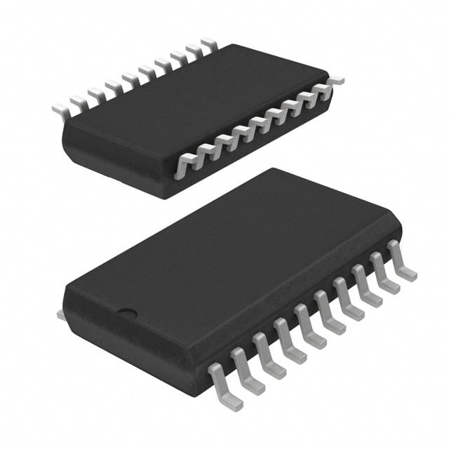
| 描述 | IC ADC 10BIT 8-CHAN SRL 20-SOIC模数转换器 - ADC 10-Bit 8-Ch 350kSPS Serial |
| 产品分类 | |
| 品牌 | Analog Devices |
| 产品手册 | |
| 产品图片 |
|
| rohs | 符合RoHS无铅 / 符合限制有害物质指令(RoHS)规范要求 |
| 产品系列 | 数据转换器IC,模数转换器 - ADC,Analog Devices AD7812YRZ- |
| 数据手册 | |
| 产品型号 | AD7812YRZ |
| 产品目录页面 | |
| 产品种类 | 模数转换器 - ADC |
| 位数 | 10 |
| 供应商器件封装 | 20-SOIC W |
| 分辨率 | 10 bit |
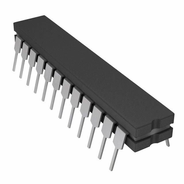
| 包装 | 管件 |
| 商标 | Analog Devices |
| 安装类型 | 表面贴装 |
| 安装风格 | SMD/SMT |
| 封装 | Tube |
| 封装/外壳 | 20-SOIC(0.295",7.50mm 宽) |
| 封装/箱体 | SOIC-20 |
| 工作温度 | -40°C ~ 105°C |
| 工作电源电压 | 5 V |
| 工厂包装数量 | 37 |
| 接口类型 | Serial (3-Wire, 5-Wire) |
| 数据接口 | DSP,串行 |
| 最大功率耗散 | 10.5 mW |
| 最大工作温度 | + 105 C |
| 最小工作温度 | - 40 C |
| 标准包装 | 37 |
| 特性 | - |
| 电压参考 | Internal, External |
| 电压源 | 单电源 |
| 系列 | AD7812 |
| 结构 | SAR |
| 转换器数 | 1 |
| 转换器数量 | 1 |
| 转换速率 | 350 kS/s |
| 输入数和类型 | 8 个单端,单极7 伪差分,单极 |
| 输入类型 | Single-Ended |
| 通道数量 | 8 Channel |
| 采样率(每秒) | 350k |


- 商务部:美国ITC正式对集成电路等产品启动337调查
- 曝三星4nm工艺存在良率问题 高通将骁龙8 Gen1或转产台积电
- 太阳诱电将投资9.5亿元在常州建新厂生产MLCC 预计2023年完工
- 英特尔发布欧洲新工厂建设计划 深化IDM 2.0 战略
- 台积电先进制程称霸业界 有大客户加持明年业绩稳了
- 达到5530亿美元!SIA预计今年全球半导体销售额将创下新高
- 英特尔拟将自动驾驶子公司Mobileye上市 估值或超500亿美元
- 三星加码芯片和SET,合并消费电子和移动部门,撤换高东真等 CEO
- 三星电子宣布重大人事变动 还合并消费电子和移动部门
- 海关总署:前11个月进口集成电路产品价值2.52万亿元 增长14.8%


PDF Datasheet 数据手册内容提取
a 2.7 V to 5.5 V, 350 kSPS, 10-Bit 4-/8-Channel Sampling ADCs AD7811/AD7812 FEATURES The control registers of the AD7811 and AD7812 allow the 10-Bit ADC with 2.3 (cid:1)s Conversion Time input channels to be configured as single-ended or pseudo The AD7811 has Four Single-Ended Inputs that differential. The control register also features a software convert Can Be Configured as Three Pseudo Differential start and a software power-down. Two of these devices can Inputs with Respect to a Common, or as Two Inde- share the same serial bus and may be individually addressed in pendent Pseudo Differential Channels a multipackage application by hardwiring the device address pin. The AD7812 has Eight Single-Ended Inputs that Can The AD7811 is available in a small, 16-lead 0.3" wide, plastic Be Configured as Seven Pseudo Differential Inputs dual-in-line package (mini-DIP), in a 16-lead 0.15" wide, Small with Respect to a Common, or as Four Independent Outline IC (SOIC) and in a 16-lead, Thin Shrink Small Out- Pseudo Differential Channels line Package (TSSOP). The AD7812 is available in a small, Onboard Track and Hold 20-lead 0.3" wide, plastic dual-in-line package (mini-DIP), in a Onboard Reference 2.5 V (cid:2) 2.5% 20-lead, Small Outline IC (SOIC) and in a 20-lead, Thin Shrink Operating Supply Range: 2.7 V to 5.5 V Small Outline Package (TSSOP). Specifications at 2.7 V–3.6 V and 5 V (cid:2) 10% DSP-/Microcontroller-Compatible Serial Interface PRODUCT HIGHLIGHTS High Speed Sampling and Automatic Power-Down Modes 1. Low Power, Single Supply Operation Package Address Pin on the AD7811 and AD7812 Allows Both the AD7811 and AD7812 operate from a single 2.7 V Sharing of the Serial Bus in Multipackage Applications to 5.5 V supply and typically consume only 10 mW of power. Input Signal Range: 0 V to V The power dissipation can be significantly reduced at REF Reference Input Range: 1.2 V to V lower throughput rates by using the automatic power- DD Qualified for Automotive Applications down mode e.g., 315 µW @ 10 kSPS, VDD = 3 V—see Power vs. Throughput. GENERAL DESCRIPTION The AD7811 and AD7812 are high speed, low power, 10-bit 2. 4-/8-Channel, 10-Bit ADC A/D converters that operate from a single 2.7 V to 5.5 V supply. The AD7811 and AD7812 have four and eight single-ended The devices contain a 2.3 µs successive approximation A/D input channels respectively. These inputs can be configured converter, an on-chip track/hold amplifier, a 2.5 V on-chip refer- as pseudo differential inputs by using the Control Register. ence and a high speed serial interface that is compatible with the 3. On-chip 2.5 V (±2.5%) reference circuit that is powered serial interfaces of most DSPs (Digital Signal Processors) and down when using an external reference. microcontrollers. The user also has the option of using an exter- nal reference by connecting it to the VREF pin and setting the 4. Hardware and Software Control EXTREF bit in the control register. The VREF pin may be tied The AD7811 and AD7812 provide for both hardware and to VDD. At slower throughput rates the power-down mode may software control of Convert Start and Power-Down. be used to automatically power down between conversions. FUNCTIONAL BLOCK DIAGRAMS CREF REFIN VDD AGND DGND CREF REFIN VDD AGND DGND 1R.2E3FV AD7811 1R.2E3FV AD7812 CLOCK CLOCK BUF OSC DOUT BUF OSC DOUT REDCISHTDARARICBGUETION SPEORRIATL DRTFIFNSS VVVIIINNN123 REDCISHTDARARICBGUETION SPEORRIATL DRTFIFNSS VVVVIIIINNNN1234 MUX VDD/3 COMP COLNOTGRICOL SCLK VVVVVIIIIINNNNN45678 MUX VDD/3 COMP COLONTGRICOL SCLK A0 CONVST A0 CONVST REV. C Information furnished by Analog Devices is believed to be accurate and reliable. However, no responsibility is assumed by Analog Devices for its use, nor for any infringements of patents or other rights of third parties One Technology Way, P.O. Box 9106, Norwood, MA 02062-9106, U.S.A. which may result from its use. No license is granted by implication or Tel: 781/329-4700 World Wide Web Site: http://www.analog.com otherwise under any patent or patent rights of Analog Devices. Fax: 781/326-8703 © Analog Devices, Inc., 2014
AD7811/AD7812–SPECIFICATIONS (V = 2.7 V to 3.6 V, V = 5 V (cid:2) 10%, GND = 0 V, V = V DD DD REF DD [EXT]. All specifications –40(cid:3)C to +105(cid:3)Cunless otherwise noted.) Parameter Y Version Unit Test Conditions/Comments DYNAMIC PERFORMANCE f = 30 kHz Any Channel, f = 350 kHz IN SAMPLE Signal to (Noise + Distortion) Ratio1 58 dB min V Internal or External REF Total Harmonic Distortion (THD)1 –66 dB max Peak Harmonic or Spurious Noise1 –80 dB typ Intermodulation Distortion1, 2 fa = 29 kHz, fb = 30 kHz Second Order Terms –67 dB max Third Order Terms –67 dB max Channel-to-Channel Isolation1, 2 –80 dB typ f = 20 kHz IN DC ACCURACY Any Channel Resolution 10 Bits Minimum Resolution for Which No Missing Codes are Guaranteed 10 Bits Relative Accuracy1 ±1 LSB max Differential Nonlinearity1 ±1 LSB max Gain Error1 ±2 LSB max Gain Error Match1 ±0.75 LSB max Offset Error1 ±2 LSB max Offset Error Match1 ±0.75 LSB max ANALOG INPUT Input Voltage Range 0 V min V V max REF Input Leakage Current2 ±1 µA max Input Capacitance2 20 pF max REFERENCE INPUTS2 V Input Voltage Range 1.2 V min REF V V max DD Input Leakage Current ±3 µA max Input Capacitance 20 pF max ON-CHIP REFERENCE Nominal 2.5 V Reference Error ±2.5 % max Temperature Coefficient 50 ppm/°C typ LOGIC INPUTS2 V ,Input High Voltage 2.4 V min V = 5 V ± 10% INH DD V , Input Low Voltage 0.8 V max V = 5 V ± 10% INL DD V ,Input High Voltage 2 V min V = 3 V ± 10% INH DD V , Input Low Voltage 0.4 V max V = 3 V ± 10% INL DD Input Current, I ±1 µA max Typically 10 nA, V = 0 V to V IN IN DD Input Capacitance, C 8 pF max IN LOGIC OUTPUTS Output High Voltage, V I = 200 µA OH SOURCE 4 V min V = 5 V ± 10% DD 2.4 V min V = 3 V ± 10% DD Output Low Voltage, V I = 200 µA OL SINK 0.4 V max High Impedance Leakage Current ±1 µA max High Impedance Capacitance 15 pF max CONVERSION RATE Conversion time 2.3 µs max Track/Hold Acquisition Time1 200 ns max –2– REV. B
AD7811/AD7812 Parameter Y Version Unit Test Conditions/Comments POWER SUPPLY V 2.7 V min For Specified Performance DD 5.5 V max I Digital Inputs = 0 V or V DD DD Normal Operation 3.5 mA max Power-Down Full Power-Down 1 µA max Partial Power-Down (Internal Ref) 350 µA max See Power-Up Times Section Power Dissipation V = 3 V DD Normal Operation 10.5 mW max Auto Full Power-Down See Power vs. Throughput Section Throughput 1 kSPS 31.5 µW max Throughput 10 kSPS 315 µW max Throughput 100 kSPS 3.15 mW max Partial Power-Down (Internal Ref) 1.05 mW max Full Power-Down 3 µW max NOTES 1See Terminology. 2Sample tested during initial release and after any redesign or process change that may affect this parameter. Specifications subject to change without notice. TIMING CHARACTERISTICS1, 2 (V = 2.7 V to 5.5 V, V = V [EXT] unless otherwise noted) DD REF DD Parameter Y Version Unit Conditions/Comments t 1.5 µs (max) Power-Up Time of AD7811/AD7812 after Rising Edge of CONVST POWER-UP t 2.3 µs (max) Conversion Time 1 t 20 ns (min) CONVST Pulsewidth 2 t 25 ns (min) SCLK High Pulsewidth 3 t 25 ns (min) SCLK Low Pulsewidth 4 t 3 5 ns (min) RFS Rising Edge to SCLK Rising Edge Setup Time 5 t 3 5 ns (min) TFS Falling Edge to SCLK Falling Edge Setup Time 6 t 3 10 ns (max) SCLK Rising Edge to Data Out Valid 7 t 10 ns (min) DIN Data Valid to SCLK Falling Edge Setup Time 8 t 5 ns (min) DIN Data Valid after SCLK Falling Edge Hold Time 9 t 3, 4 20 ns (max) SCLK Rising Edge to D High Impedance 10 OUT t 100 ns (min) DOUT High Impedance to CONVST Falling Edge 11 NOTES 1Sample tested to ensure compliance. 2See Figures 16, 17 and 18. 3These numbers are measured with the load circuit of Figure 1. They are defined as the time required for the o/p to cross 0.8 V or 2.4 V for V = 5 V ± 10% and DD 0.4 V or 2 V for V = 3 V ± 10%. DD 4Derived from the measured time taken by the data outputs to change 0.5 V when loaded with the circuit of Figure 1. The measured number is then extrapolated back to remove the effects of charging or discharging the 50 pF capacitor. This means that the time, t , quoted in the Timing Characteristics is the true bus relinquish 11 time of the part and as such is independent of external bus loading capacitances. Specifications subject to change without notice. 200(cid:1)A IOL TO OUTPUT 2.1V PIN CL 50pF 200(cid:1)A IOH Figure 1.Load Circuit for Digital Output Timing Specifications REV. C –3–
AD7811/AD7812 ABSOLUTE MAXIMUM RATINGS* SOIC Package, Power Dissipation . . . . . . . . . . . . . . . 450 mW VDD to DGND . . . . . . . . . . . . . . . . . . . . . . . . . –0.3 V to +7 V θJA Thermal Impedance . . . . . . . . . . . . . . . . . . . . . 75°C/W Digital Input Voltage to DGND (CONVST, SCLK, RFS, TFS, Lead Temperature, Soldering DIN, A0) . . . . . . . . . . . . . . . . . . . . . . . –0.3 V, VDD + 0.3 V Vapor Phase (60 sec) . . . . . . . . . . . . . . . . . . . . . . .215°C Digital Output Voltage to DGND (DOUT) Infrared (15 sec) . . . . . . . . . . . . . . . . . . . . . . . . . .220°C . . . . . . . . . . . . . . . . . . . . . . . . . . . . . . .–0.3 V, VDD + 0.3 V TSSOP Package, Power Dissipation . . . . . . . . . . . . . 450 mW REFIN to AGND . . . . . . . . . . . . . . . . . . . –0.3 V, VDD + 0.3 V θJA Thermal Impedance . . . . . . . . . . . . . . . . . . . . 115°C/W Analog Inputs Lead Temperature, Soldering VIN1–VIN4 (AD7811) . . . . . . . . . . . . . .–0.3 V, VDD + 0.3 V Vapor Phase (60 sec) . . . . . . . . . . . . . . . . . . . . . . .215°C VIN1–VIN8 (AD7812) . . . . . . . . . . . . . .–0.3 V, VDD + 0.3 V Infrared (15 sec) . . . . . . . . . . . . . . . . . . . . . . . . . .220°C Storage Temperature Range . . . . . . . . . . . . –65°C to +150°C Junction Temperature . . . . . . . . . . . . . . . . . . . . . . . . . .150°C *Stresses above those listed under Absolute Maximum Ratings may cause perma- nent damage to the device. This is a stress rating only; functional operation of the Plastic DIP Package, Power Dissipation . . . . . . . . . . 450 mW device at these or any other conditions above those listed in the operational θ Thermal Impedance . . . . . . . . . . . . . . . . . . . . 105°C/W sections of this specification is not implied. Exposure to absolute maximum rating JA Lead Temperature, (Soldering 10 sec) . . . . . . . . . . . .260°C conditions for extended periods may affect device reliability. ORDERING GUIDE Linearity Package Package Model Error Descriptions Options AD7811YN ±1 LSB 16-Lead Plastic DIP N-16 AD7811YR ±1 LSB 16-Lead Small Outline IC (SOIC) R-16A AD7811YRU ±1 LSB 16-Lead Thin Shrink Small Outline Package (TSSOP) RU-16 AD7812YN ±1 LSB 20-Lead Plastic DIP N-20 AD7812YR ±1 LSB 20-Lead Small Outline IC (SOIC) R-20A AD7812YRU ±1 LSB 20-Lead Thin Shrink Small Outline Package (TSSOP) RU-20 CAUTION ESD (electrostatic discharge) sensitive device. Electrostatic charges as high as 4000 V readily WARNING! accumulate on the human body and test equipment and can discharge without detection. Although the AD7811/AD7812 features proprietary ESD protection circuitry, permanent damage may occur on devices subjected to high-energy electrostatic discharges. Therefore, proper ESD precautions are recommended to avoid performance degradation or loss of functionality. ESD SENSITIVE DEVICE –4– REV. B
AD7811/AD7812 PIN CONFIGURATIONS DIP/SOIC/TSSOP VREF 1 16 VDD VREF 1 20 VDD CREF 2 15 CONVST CREF 2 19 CONVST VIN1 3 AD7811 14 SCLK VIN1 3 18 SCLK AGND 4 13 DIN AGND 4 17 DIN TOP VIEW VIN2 5 (Not to Scale) 12 DOUT VIN2 5 AD7812 16 DOUT VIN3 6 11 RFS VIN3 6 (NToOt Pto V SIEcaWle) 15 RFS VIN4 7 10 TFS VIN4 7 14 TFS A0 8 9 DGND VIN5 8 13 DGND VIN6 9 12 A0 VIN7 10 11 VIN8 PIN FUNCTION DESCRIPTIONS Pin(s) Pin(s) AD7811 AD7812 Mnemonic Description 1 1 V An external reference input can be applied here. When using an external precision REF reference or V the EXTREF bit in the control register must be set to logic one. The DD external reference input range is 1.2 V to V . DD 2 2 C Reference Capacitor. A capacitor (10 nF) is connected here to improve the noise REF performance of the on-chip reference. 3, 5–7 3, 5–11 V –V Analog Inputs. The analog input range is 0 V to V . IN1 IN4(8) REF 4 4 AGND Analog Ground. Ground reference for track/hold, comparator, on-chip reference and DAC. 8 12 A0 Package Address Pin. This Logic Input can be hardwired high or low. When used in conjunction with the package address bit in the control register this input allows two devices to share the same serial bus. For example a twelve channel solution can be achieved by using the AD7811 and the AD7812 on the same serial bus. 9 13 DGND Digital Ground. Ground reference for digital circuitry. 10 14 TFS Transmit Frame Sync. The falling edge of this Logic Input tells the part that a new control byte should be shifted in on the next 10 falling edges of SCLK. 11 15 RFS Receive Frame Sync. The rising edge of this Logic Input is used to enable a counter in the serial interface. It is used to provide compatibility with DSPs which use a continuous serial clock and framing signal. In multipackage applications the RFS Pin can also be used as a serial bus select pin. The serial interface will ignore the SCLK until it receives a rising edge on this input. The counter is reset at the end of a serial read operation. 12 16 DOUT Serial Data Output. Serial data is shifted out on this pin on the rising edge of the serial clock. The output enters a High impedance condition on the rising edge of the 11th SCLK pulse. 13 17 DIN Serial Data Input. The control byte is read in at this input. In order to complete a serial write operation 13 SCLK pulses need to be provided. Only the first 10 bits are shifted in—see Serial Interface section. 14 18 SCLK Serial Clock Input. An external serial clock is applied to this input to obtain serial data from the AD7811/AD7812 and also to latch data into the AD7811/AD7812. Data is clocked out on the rising edge of SCLK and latched in on the falling edge of SCLK. 15 19 CONVST Convert Start. This is an edge triggered logic input. The Track/Hold goes into its Hold Mode on the falling edge of this signal and a conversion is initiated. The state of this pin at the end of conversion also determines whether the part is powered down or not. See operating modes section of this data sheet. 16 20 V Positive Supply Voltage 2.7 V to 5.5 V. DD REV. B –5–
AD7811/AD7812 TERMINOLOGY usually distanced in frequency from the original sine waves Signal to (Noise + Distortion) Ratio while the third order terms are usually at a frequency close to This is the measured ratio of signal to (noise + distortion) at the the input frequencies. As a result, the second and third order output of the A/D converter. The signal is the rms amplitude of terms are specified separately. The calculation of the inter- the fundamental. Noise is the rms sum of all nonfundamental modulation distortion is as per the THD specification where it is signals up to half the sampling frequency (f /2), excluding dc. the ratio of the rms sum of the individual distortion products to S The ratio is dependent upon the number of quantization levels the rms amplitude of the fundamental expressed in dBs. in the digitization process; the more levels, the smaller the Channel-to-Channel Isolation quantization noise. The theoretical signal to (noise + distor- Channel-to-channel isolation is a measure of the level of tion) ratio for an ideal N-bit converter with a sine wave input crosstalk between channels. It is measured by applying a full- is given by: scale 20kHz sine wave signal to all nonselected input channels Signal to (Noise + Distortion) = (6.02N + 1.76) dB and determining how much that signal is attenuated in the selected Thus for a 10-bit converter, this is 62dB. channel. The figure given is the worst case across all four or eight channels for the AD7811 and AD7812 respectively. Total Harmonic Distortion Total harmonic distortion (THD) is the ratio of the rms sum of Relative Accuracy harmonics to the fundamental. For the AD7811 and AD7812 Relative accuracy, or endpoint nonlinearity, is the maximum it is defined as: deviation from a straight line passing through the endpoints of the ADC transfer function. V2+V2+V2+V2+V2 Differential Nonlinearity THD(dB)=20log 2 3 4 5 6 This is the difference between the measured and the ideal V 1 1LSB change between any two adjacent codes in the ADC. where V is the rms amplitude of the fundamental and V , V , 1 2 3 Offset Error V , V and V are the rms amplitudes of the second through the 4 5 6 This is the deviation of the first code transition (0000...000) sixth harmonics. to (0000...001) from the ideal, i.e., AGND + 1 LSB. Peak Harmonic or Spurious Noise Offset Error Match Peak harmonic or spurious noise is defined as the ratio of the This is the difference in Offset Error between any two channels. rms value of the next largest component in the ADC output spectrum (up to f /2 and excluding dc) to the rms value of the Gain Error S This is the deviation of the last code transition (1111...110) fundamental. Normally, the value of this specification is to (1111...111) from the ideal, i.e., V – 1 LSB, after the determined by the largest harmonic in the spectrum, but for REF offset error has been adjusted out. parts where the harmonics are buried in the noise floor, it will be a noise peak. Gain Error Match This is the difference in Gain Error between any two channels. Intermodulation Distortion With inputs consisting of sine waves at two frequencies, fa and Track/Hold Acquisition Time fb, any active device with nonlinearities will create distortion Track/hold acquisition time is the time required for the output products at sum and difference frequencies of mfa ± nfb where of the track/hold amplifier to reach its final value, within m, n = 0, 1, 2, 3, etc. Intermodulation terms are those for ±1/2 LSB, after the end of conversion (the point at which the which neither m nor n are equal to zero. For example, the track/hold returns to track mode). It also applies to situations second order terms include (fa + fb) and (fa – fb), while the where a change in the selected input channel takes place or third order terms include (2fa + fb), (2fa – fb), (fa + 2fb) and where there is a step input change on the input voltage applied (fa – 2fb). to the selected V input of the AD7811 or AD7812. It means IN that the user must wait for the duration of the track/hold acquisi- The AD7811 and AD7812 are tested using the CCIF standard tion time after the end of conversion or after a channel change/ where two input frequencies near the top end of the input step input change to V before starting another conversion, to bandwidth are used. In this case, the second and third order IN ensure that the part operates to specification. terms are of different significance. The second order terms are –6– REV. B
AD7811/AD7812 Control Register (AD7811) The Control Register is a 10-bit-wide, write only register. The Control Register is written to when the AD7811 receives a falling edge on its TFS pin. The AD7811 will maintain the same configuration until a new control byte is written to the part. The control register can be written to at the same time data is being read. This latter feature enhances throughput rates when software control is being used or when the analog input channels are being changed frequently. The power-up default register contents are all zeros; therefore, when the supplies are connected, the AD7811 is powered down by default. Control Register AD7811 9 0 X* A0 PD1 PD0 V /AGND DIFF/SGL CH1 CH0 CONVST EXTREF IN4 *This is a don’t care bit. A0 This is the package address bit. It is used in conjunction with the package address pin to allow two AD7811s to share the same serial bus. The AD7811 can also share the same serial bus with the AD7812. When a control word is written to the control register of the AD7811 the control word is ignored if the package address bit in the con- trol byte does not match how the package address pin is hardwired. Only the serial port of the device that received the last valid control byte, i.e., the address bit matched the address pin, will attempt to drive the serial bus on the next serial read. When the part powers up this bit is set to 0. PD1, PD0 These bits allow the AD7811 to be fully powered down and powered up. Bit combinations PD1 = PD0 = 0 and PD1 = PD0 = 1 override the automatic power-down decision at the end of conversion. These bits also decide the power-down mode when the AD7811 enters a power-down at the end of a conversion. There are two power-down modes—Full Power-Down and Partial Power-Down. See Power-Down Options section of this data sheet. PD1 PD0 Description 0 0 Full Power-Down of the AD7811 0 1 Partial Power-Down at the End of Conversion 1 0 Full Power-Down at the End of Conversion 1 1 Power-Up the AD7811 V /AGND The DIF/SGL bit in the control register must be set to 0 to use this option otherwise this bit is ignored. Setting IN4 V /AGND to 0 configures the analog inputs of the AD7811 as four single-ended analog inputs referenced to IN4 analog ground (AGND). By setting this bit to 1 the input channels V to V are configured as three pseudo- IN1 IN3 differential channels with respect to V —see Table I. IN4 DIF/SGL This bit is used to configure the analog inputs as single ended or pseudo differential pairs. By setting this bit to 0 the analog inputs can be configured as single ended with respect to AGND, or pseudo differential with respect to V as explained above. Setting this bit to 1 configures the analog input channels as two pseudo differential pairs IN4 V /V and V /V —see Table I. IN1 IN2 IN3 IN4 CH1, CH0 These bits are used in conjunction with V /AGND and DIF/SGL to select an analog input channel. The table IN4 shows how the various channel selections are made—see Table I. CONVST Setting this bit to a logic one initiates a conversion. A conversion is initiated 400 ns after a write to the control register has taken place. This allows a signal to be acquired even if the channel is changed and a conversion initiated in the same serial write. The bit is reset after the end of a conversion. EXTREF This bit must be set to a logic one if the user wishes to use an external reference or use V as the reference. DD When the external reference is selected the on chip reference circuitry powers down. REV. B –7–
AD7811/AD7812 Control Register (AD7812) The Control Register is a 10-bit-wide, write only register. The Control Register is written to when the AD7812 receives a falling edge on its TFS pin. The AD7812 will maintain the same configuration until a new control byte is written to the part. The control register can be written to at the same time data is being read. This latter feature enhances throughput rates when software control is being used or when the analog input channels are being changed frequently. The power-up default register contents are all zeros; therefore, when the supplies are connected, the AD7812 is powered down by default. Control Register AD7812 9 0 A0 PD1 PD0 V /AGND DIFF/SGL CH2 CH1 CH0 CONVST EXTREF IN8 A0 This is the package address bit. It is used in conjunction with the package address pin to allow two AD7812s to share the same serial bus. The AD7812 can also share the same serial bus with the AD7811. When a control word is written to the control register of the AD7812 the control word is ignored if the package address bit in the con- trol byte does not match how the package address pin is hardwired. Only the serial port of the device which received the last valid control byte, i.e., the address bit matched the address pin, will attempt to drive the serial bus on the next serial read. When the part powers up this bit is set to 0. PD1, PD0 These bits allow the AD7812 to be fully powered down and powered up. Bit combinations PD1 = PD0 = 0 and PD1 = PD0 = 1 override the automatic power-down decision at the end of conversion. These bits also decide the power-down mode when the AD7812 enters a power-down at the end of a conversion. There are two power-down modes—Full Power-Down and Partial Power-Down. See Power-Down section of this data sheet. PD1 PD0 Description 0 0 Full Power-Down of the AD7812 0 1 Partial Power-Down at the End of Conversion 1 0 Full Power-Down at the End of Conversion 1 1 Power-Up the AD7812 V /AGND The DIF/SGL bit in the control register must be set to 0 in order to use this option otherwise this bit is ignored. IN8 Setting V /AGND to 0 configures the analog inputs of the AD7812 as eight single-ended analog inputs IN8 referenced to analog ground (AGND). By setting this bit to 1 the input channels V to V are configured IN1 IN7 as seven pseudo differential channels with respect to V —see Table II. IN8 DIF/SGL This bit is used to configure the analog inputs as single ended or pseudo differential pairs. By setting this bit to 0 the analog inputs can be configured as single ended with respect to AGND, or pseudo differential with respect to V as explained above. Setting this bit to 1 configures the analog input channels as four pseudo differential pairs IN8 V /V , V /V , V /V and V /V —see Table II. IN1 IN2 IN3 IN4 IN5 IN6 IN7 IN8 CH2, CH1, CH0 These bits are used in conjunction with V /AGND and DIF/SGL to select an analog input channel. Table II IN8 shows how the various channel selections are made. CONVST Setting this bit to a logic one initiates a conversion. A conversion is initiated 400 ns after a write to the control register has taken place. This allows a signal to be acquired even if the channel is changed and a conversion initi- ated in the same write operation. The bit is reset after the end of a conversion. EXTREF This bit must be set to a logic one if the user wishes to use an external reference or use V as the reference. DD When the external reference is selected the on-chip reference circuitry powers down and the current consumption is reduced by about 1 mA. –8– REV. B
AD7811/AD7812 Table I. AD7811 Channel Configurations V /AGND DIF/SGL CH1 CH0 Description IN4 0 0 0 0 V Single-Ended with Respect to AGND IN1 0 0 0 1 V Single-Ended with Respect to AGND IN2 0 0 1 0 V Single-Ended with Respect to AGND IN3 0 0 1 1 V Single-Ended with Respect to AGND IN4 1 0 0 0 V Pseudo Differential with Respect to V IN1 IN4 1 0 0 1 V Pseudo Differential with Respect to V IN2 IN4 1 0 1 0 V Pseudo Differential with Respect to V IN3 IN4 X 1 0 0 V (+) Pseudo Differential with Respect to V (–) IN1 IN2 X 1 0 1 V (+) Pseudo Differential with Respect to V (–) IN3 IN4 X 1 1 0 Internal Test. SAR Input Equal to V /2 REF X 1 1 1 Internal Test. SAR Input Equal to V REF Table II. AD7812 Channel Configurations V /AGND DIF/SGL CH2 CH1 CH0 Description IN8 0 0 0 0 0 V Single-Ended with Respect to AGND IN1 0 0 0 0 1 V Single-Ended with Respect to AGND IN2 0 0 0 1 0 V Single-Ended with Respect to AGND IN3 0 0 0 1 1 V Single-Ended with Respect to AGND IN4 0 0 1 0 0 V Single-Ended with Respect to AGND IN5 0 0 1 0 1 V Single-Ended with Respect to AGND IN6 0 0 1 1 0 V Single-Ended with Respect to AGND IN7 0 0 1 1 1 V Single-Ended with Respect to AGND IN8 1 0 0 0 0 V Pseudo Differential with Respect to V IN1 IN8 1 0 0 0 1 V Pseudo Differential with Respect to V IN2 IN8 1 0 0 1 0 V Pseudo Differential with Respect to V IN3 IN8 1 0 0 1 1 V Pseudo Differential with Respect to V IN4 IN8 1 0 1 0 0 V Pseudo Differential with Respect to V IN5 IN8 1 0 1 0 1 V Pseudo Differential with Respect to V IN6 IN8 1 0 1 1 0 V Pseudo Differential with Respect to V IN7 IN8 X 1 0 0 0 V (+) Pseudo Differential with Respect to V (–) IN1 IN2 X 1 0 0 1 V (+) Pseudo Differential with Respect to V (–) IN3 IN4 X 1 0 1 0 V (+) Pseudo Differential with Respect to V (–) IN5 IN6 X 1 0 1 1 V (+) Pseudo Differential with Respect to V (–) IN7 IN8 X 1 1 0 0 Internal Test. SAR Input Equal to V /2 REF X 1 1 0 1 Internal Test. SAR Input Equal to V REF REV. B –9–
AD7811/AD7812 CIRCUIT DESCRIPTION SUPPLY Converter Operation 2.7V TO 5.5V THREE-WIRE The AD7811 and AD7812 are successive approximation analog- 10(cid:1)F 0.1(cid:1)F 10nF SERIAL INTERFACE to-digital converters based around a charge redistribution DAC. The ADCs can convert analog input signals in the range 0 V to V . Figures 2 and 3 show simplified schematics of the ADC. VDD VREF CREF DD Figure 2 shows the ADC during its acquisition phase. SW2 is SCLK closed and SW1 is in position A, the comparator is held in a VIN1 DOUT balanced condition and the sampling capacitor acquires the VIN2 AD7811/ 0V TO signal on VIN. VREF AD7812 DIN µC/µP INPUT VIN4(8) CONVST CHARGE REDISTRIBUTION DAC RFS SAMPLING A CAPACITOR AGND TFS VIN CONTROL SW1 LOGIC DGND A0 B ACQUISITION PHASE SW2 COMPARATOR Figure 4. Typical Connection Diagram AGND CLOCK OSC VDD/3 Analog Input Figure 2.ADC Acquisition Phase Figure 5 shows an equivalent circuit of the analog input struc- ture of the AD7811 and AD7812. The two diodes D1 and D2 When the ADC starts a conversion, see Figure 3, SW2 will provide ESD protection for the analog inputs. Care must be open and SW1 will move to position B causing the comparator taken to ensure that the analog input signal never exceeds the to become unbalanced. The Control Logic and the Charge supply rails by more than 200 mV. This will cause these diodes Redistribution DAC are used to add and subtract fixed amounts to become forward biased and start conducting current into of charge from the sampling capacitor to bring the comparator the substrate. 20 mA is the maximum current these diodes can back into a balanced condition. When the comparator is rebal- conduct without causing irreversible damage to the part. How- anced, the conversion is complete. The Control Logic generates ever, it is worth noting that a small amount of current (1 mA) the ADC output code. Figure 10 shows the ADC transfer being conducted into the substrate due to an overvoltage on an function. unselected channel can cause inaccurate conversions on a selected channel. The capacitor C2 in Figure 5 is typically about CHARGE 4 pF and can primarily be attributed to pin capacitance. The REDISTRIBUTION resistor R1 is a lumped component made up of the on resistance DAC SAMPLING of a multiplexer and a switch. This resistor is typically about A CAPACITOR 125 Ω. The capacitor C1 is the ADC sampling capacitor and VIN CONTROL SW1 LOGIC has a capacitance of 3.5 pF. B CONVERSION AGND PHASE SW2 COMPARATOR CLOCK VDD OSC FigureV D3D./ 3ADC Conversion Phase D1 12R51(cid:4) 3.C51pF VIN VDD/3 TYPICAL CONNECTION DIAGRAM Figure 4 shows a typical connection diagram for the AD7811/ C4p2F D2 AD7812. The AGND and DGND are connected together at CONVERSION PHASE – SWITCH OPEN TRACK PHASE – SWITCH CLOSED the device for good noise suppression. The serial interface is implemented using three wires with RFS/TFS connected to CONVST see Serial Interface section for more details. VREF is Figure 5.Equivalent Analog Input Circuit connected to a well decoupled V pin to provide an analog DD The analog inputs on the AD7811 and AD7812 can be config- input range of 0 V to V . If the AD7811 or AD7812 is not DD ured as single ended with respect to analog ground (AGND), sharing a serial bus with another AD7811 or AD7812 then A0 as pseudo differential with respect to a common, and also as (package address pin) should be hardwired low. The default pseudo differential pairs—see Control Register section. power up value of the package address bit in the control register is 0. For applications where power consumption is of concern, the automatic power down at the end of a conversion should be used to improve power performance. See Power-Down Options section of the data sheet. –10– REV. B
AD7811/AD7812 An example of the pseudo differential scheme using the AD7811 Figure 8 shows the equivalent charging circuit for the sampling is shown in Figure 6. The relevant bits in the AD7811 Control capacitor when the ADC is in its acquisition phase. R2 repre- Register are set as follows DIF/SGL = 1, CH1 = CH2 = 0, i.e., sents the source impedance of a buffer amplifier or resistive V pseudo differential with respect to V . The signal is network; R1 is an internal multiplexer resistance, and C1 is the IN1 IN2 applied to V but in the pseudo differential scheme the sam- sampling capacitor. During the acquisition phase the sampling IN1 pling capacitor is connected to V during conversion and not capacitor must be charged to within a 1/2 LSB of its final value. IN2 AGND as described in the Converter Operation section. This The time it takes to charge the sampling capacitor (T ) is CHARGE input scheme can be used to remove offsets that exist in a sys- given by the following formula: tem. For example, if a system had an offset of 0.5 V the offset T = 7.6 × (R2 + 125 Ω) × 3.5 pF could be applied to V and the signal applied to V . This has CHARGE IN2 IN1 the effect of offsetting the input span by 0.5 V. It is only pos- R1 sible to offset the input span when the reference voltage is less R2 VIN+ 125(cid:4) than V –OFFSET. DD C1 SAMPLING 3.5pF CAPACITOR CHARGE REDISTRIBUTION Figure 8. Equivalent Sampling Circuit DAC SAMPLING For small values of source impedance, the settling time associ- VIN1 VIN+ CAPACITOR ated with the sampling circuit (100 ns) is, in effect, the acquisi- VIN1 CONTROL tion time of the ADC. For example, with a source impedance VOFFSET LOGIC CONVERSION (R2) of 10 Ω the charge time for the sampling capacitor is VIN– PHASE COMPARATOR approximately 4 ns. The charge time becomes significant for VOFFSET VIN2 COLOSCCK source impedances of 2 kΩ and greater. VDD/3 AC Acquisition Time In ac applications it is recommended to always buffer analog Figure 6.Pseudo Differential Input Scheme input signals. The source impedance of the drive circuitry must When using the pseudo differential input scheme the signal on be kept as low as possible to minimize the acquisition time of VIN2 must not vary by more than a 1/2 LSB during the conver- the ADC. Large values of source impedance will cause the THD sion process. If the signal on VIN2 varies during conversion, the to degrade at high throughput rates. In addition, better perfor- conversion result will be incorrect. In single-ended mode the mance can generally be achieved by using an External 1 nF sampling capacitor is always connected to AGND during con- capacitor on V . IN version. Figure 7 shows the AD7811/AD7812 pseudo differen- tial input being used to make a unipolar dc current measurement. ON-CHIP REFERENCE A sense resistor is used to convert the current to a voltage and The AD7811 and AD7812 have an on-chip 2.5 V reference the voltage is applied to the differential input as shown. circuit. The schematic in Figure 9 shows how the reference circuit is implemented. A 1.23 V bandgap reference is gained up VDD to provide a 2.5 V ± 2% reference voltage. The on-chip refer- VIN+ ence is not available externally (SW2 is open). An external refer- RSENSE AADD77881112/ eonrdceer ( t1o.2 u Vse taon V eDxDte)r cnaanl rbeefe arpenpcliee dth aet EthXeT VRREEFF p binit. iHn othwee vceorn i-n VIN– trol register (Bit 0) must first be set to a Logic 1. When EXTREF RL is set to a Logic 1 SW2 will close, SW3 will open and the ampli- fier will power down. This will reduce the current consumption of the part by about 1 mA. It is possible to use two different reference voltages by selecting the on-chip reference or external Figure 7.DC Current Measurement Scheme reference. DC Acquisition Time The ADC starts a new acquisition phase at the end of a conver- CREF EXTERNAL sion and ends on the falling edge of the CONVST signal. At the CAPACITOR VREF end of a conversion a settling time is associated with the sam- SW1 pling circuit. This settling time lasts approximately 100 ns. The SW2 analog signal on V is also being acquired during this settling IN+ time. Therefore, the minimum acquisition time needed is 1.23V approximately 100 ns. 2.5V 7pF SW3 AGND Figure 9. On-Chip Reference Circuitry REV. B –11–
AD7811/AD7812 When using automatic power-down between conversions to POWER-ON-RESET improve the power performance of the part (see Power vs. If during normal operation, a power-save is performed by removing Throughput) the switch SW1 will open when the part enters its power from the AD7811 and AD7812; the user must be wary power-down mode if using the internal on-chip reference. This that a proper reset is done when power is applied to the part provides a high impedance discharge path for the external again. To ensure proper power-on-reset, we recommend that capacitor (see Figure 9). A typical value of external capacitance both PD bits are set to 0 and then set to 1. This procedure is 10 nF. When the part is in Mode 2 Full Power-Down, because causes an internal reset to occur. the external capacitor holds its charge during power-down, the internal bandgap reference will power up more quickly after POWER-UP TIMES relatively short periods of full power-down. When operating the The AD7811 and AD7812 have a 1.5 µs power-up time when part in Mode 2 Partial Power-Down the external capacitor is not using an external reference or when powering up from partial required as the on-chip reference stays powered up while the power-down. When V is first connected, the AD7811 and DD rest of the circuitry powers down. AD7812 are in a low current mode of operation. In order to carry out a conversion the AD7811 and AD7812 must first be ADC TRANSFER FUNCTION powered up by writing to the control register of each ADC to The output coding of the AD7811 and AD7812 is straight set the power-down bits (i.e., PD1 = 1, PD0 = 1) for a full binary. The designed code transitions occur at successive inte- power-up. See the Quick Evaluation Setup section on the fol- ger LSB values (i.e., 1 LSB, 2 LSBs, etc.). The LSB size is = lowing page. V /1024. The ideal transfer characteristic for the AD7811 and REF Mode 2 Full Power-Down (PD1 = 1, PD0 = 0) AD7812 is shown in Figure 10. The power-up time of the AD7811 and AD7812 after power is first connected, or after a long period of Full Power-Down, is the time it takes the on-chip 1.23 V reference to power up plus 111...111 the time it takes to charge the external capacitor C —see REF 111...110 Figure 9. The time taken to charge C to the 10-bit level is REF CODE 111...000 1LSB = VREF/1024 gthivee np obwy etrh-eu pe qtiumatei oisn a (p7p.r6o x×i m2 aktΩel y× 1C5R2E µF)s.. IFt otark CesR E3F0 = µ s1 0to nF C 011...111 power up the on-chip reference so the total power-up time of D A either ADC in either of these conditions is 182 µs. However, 000...010 when powering down fully between conversions to achieve a 000...001 000...000 better power performance this power-up time reduces to 1.5 µs 0V 1LSB +VREF–1LSB after a relatively short period of power-down as C holds its ANALOG INPUT REF charge (see On-Chip Reference section). The AD7811 and Figure 10.AD7811 and AD7812 Transfer Characteristic AD7812 can therefore be used in Mode 2 with throughput rates of 250 kSPS and under. POWER-DOWN OPTIONS Mode 2 Partial Power-Down (PD1 = 0, PD0 = 1) The AD7811 and AD7812 provide flexible power management The power-up time of the AD7811 and AD7812 from a Partial to allow the user to achieve the best power performance for a Power-Down is 1.5 µs maximum. When using a Partial Power- given throughput rate. Down between conversions, there is no requirement to connect The power management options are selected by programming an external capacitor to the C pin because the reference REF the power-down bits (i.e., PD1 and PD0) in the control register. remains powered up. This means that the AD7811 and AD7812 Table III below summarizes the options available. When the will power up in 30 µs after the supplies are first connected as power-down bits are programmed for Mode 2 Power Down (full there is no requirement to charge an external capacitor. and partial), a rising edge on the CONVST pin will power up the part. This feature is used when powering down between POWER VS. THROUGHPUT conversions—see Power vs. Throughput. When the AD7811 By using the Automatic Power-Down (Mode 2) at the end of a and AD7812 are placed in partial power-down the on-chip conversion—see Operating Modes section of the data sheet, reference does not power down. However, the part will power superior power performance can be achieved. up more quickly after long periods of power-down when using Figure 11 shows how the Automatic Power-Down is implemented partial power-down—see Power-Up Times section. using the CONVST signal to achieve the optimum power performance for the AD7811 and AD7812. The AD7811 and Table III. AD7811/AD7812 Power-Down Options AD7812 are operated in Mode 2 and the control register Bits PD1 PD0 CONVST* Description PD1 and PD0 are set to 1 and 0 respectively for Full Power-Down, or 0 and 1 for Partial Power-Down. The duration of the CONVST 1 1 x Full Power-Up pulse is set to be equal to or less than the power-up time of the 0 0 x Full Power-Down devices—see Operating Modes section. As the throughput rate 0 1 0 Mode 2 Partial Power-Down is reduced, the device remains in its power-down state longer (Reference Stays Powered-Up) and the average power consumption over time drops accordingly. 0 1 1 No Power-Down 1 0 0 Mode 2 Full Power-Down 1 0 1 No Power-Down *This refers to the state of the CONVST signal at the end of a conversion. –12– REV. B
AD7811/AD7812 tP1O.W5(cid:1)ERs-UPtCO2.N3V(cid:1)EsRT POWER-DOWN QThUeI CscKh eEmVaAtiLc UshAoTwInO iNn FSiEgTurUe P14 shows a suggested configura- CONVST tion of the AD7812 for a first look evaluation of the part. No external reference circuit is needed as the V pin can be t REF CYCLE connected to V . The CONVST signal is connected to TFS 100(cid:1)s @ 10kSPS DD and RFS to enable the serial port. Also by selecting Mode 2 Figure 11. Automatic Power-Down operation (see Operating Modes section) the power performance For example, if the AD7811 is operated in a continuous sam- of the AD7812 can be evaluated. pling mode with a throughput rate of 10 kSPS, PD1 = 1, PD0 = 0 and using the on chip reference the power consump- SUPPLY tion is calculated as follows. The power dissipation during nor- VDD 10(cid:1)F 0.1(cid:1)F 10nF mal operation is 10.5 mW, V = 3 V. If the power-up time is DD 1.5 µs and the conversion time is 2.3 µs, the AD7811 can be said to dissipate 10.5 mW for 3.8 µs (worst-case) during each VDD VREF CREF ctiomnev eisr s1io0n0 cµysc alen. dI ft hthee a tvherroaugge hppouwt erra tde iisss i1p0a tkeSdP dSu, rtihneg c eyaccleh 0V TION PVUDTD VIN1 SCLK cycle is (3.8/100) × (10.5 mW) = 400 µW. VIN2 DOUT DIN Figure 12 shows the Power vs. Throughput Rate for automatic AD7812 full power-down. VIN7 CONVST 10 VIN8 RFS AGND TFS DGND A0 1 Figure 14.Evaluation Quick Setup V m – The setup uses a full duplex, 16-bit, serial interface protocol, R E e.g., SPI. It is possible to use 8-bit transfers by carrying out two W O consecutive read/write operations. The MSB of data is trans- P 0.1 ferred first. 1. When power is first connected to the device it is in a powered down mode of operation and is consuming only 1 µA. The AD7812 must first be configured by carrying out a serial 0.01 0 5 10 15 20 25 30 35 40 45 50 write operation. THROUGHPUT – kSPS Figure 12.AD7811/AD7812 Power vs. Throughput 2. The CONVST signal is first pulsed to enable the serial port (rising and falling edge on RFS and TFS respectively—see 0 Serial Interface section). –10 AD7811/12 3. Next, a 16-bit serial read/write operation is carried out. By 2048 POINT FFT writing 6040 Hex to the AD7812 the part is powered up, set –20 SAMPLING 357.142kHz fIN = 30.168kHz up to use external reference (i.e., VDD) and the analog input –30 V is selected. The data read from the part during this read/ IN1 s–40 write operation is invalid. B d–50 4. It is necessary to wait approximately 1.5 µs before pulsing CONVST again and initiating a conversion. The 1.5 µs is to –60 allow the AD7812 to power up correctly—see Power-Up –70 Times section. –80 5. Approximately 2.3 µs after the falling edge of CONVST, i.e., –90 after the end of the conversion, a serial read/write can take –100 place. This time 4040 Hex is written to the AD7812 and the 0 17 35 52 70 87 105 122 140 157 174 data read from the part is the result of the conversion. The FREQUENCY – kHz output code is in a straight binary format and will be left Figure 13.AD7811/AD7812 SNR justified in the 16-bit serial register (MSB clocked out first). 6. By idling the CONVST signal high or low it is possible to operate the AD7812 in Mode 1 and Mode 2 respectively. REV. B –13–
AD7811/AD7812 OPERATING MODES should occur before the end of the conversion process if the part The mode of operation of the AD7811 and AD7812 is selected is not to be powered down. A serial read can take place at any when the (logic) state of the CONVST is checked at the end of stage after the rising edge of CONVST. If a serial read is initi- a conversion. If the CONVST signal is logic high at the end ated before the end of the current conversion process (i.e., at of a conversion, the part does not power down and is operat- time “A”), the result of the previous conversion is shifted out on ing in Mode 1. If, however, the CONVST signal is brought the DOUT pin. It is possible to allow the serial read to extend logic low before the end of a conversion, the AD7811 and AD7812 beyond the end of a conversion. In this case the new data will will power down at the end of the conversion. This is Mode 2 not be latched into the output shift register until the read operation. has finished. The dynamic performance of the AD7811 and AD7812 typically degrades by up to 3 dBs while reading during Mode 1 Operation (High Speed Sampling) a conversion. If the user waits until the end of the conversion When the AD7811 and AD7812 are operated in Mode 1 they process, i.e., 2.3 µs after the falling edge of CONVST (Point are not powered down between conversions. This mode of opera- “B”) before initiating a read, the current conversion result is tion allows high throughput rates to be achieved. The timing shifted out. The serial read must finish at least 100 ns prior to diagram in Figure 16 shows how this optimum throughput rate the next falling edge of CONVST to allow the part to accurately is achieved by bringing the CONVST signal high before the end acquire the input signal. of the conversion. Mode 2 Operation (Automatic Power-Down) The sampling circuitry leaves its tracking mode and goes into When used in this mode of operation the part automatically hold on the falling edge of CONVST. A conversion is also initi- ated at this time. The conversion takes 2.3 µs to complete. At powers down at the end of a conversion. This is achieved by leaving the CONVST signal low until the end of the conversion. this point, the result of the current conversion is latched into the Because it takes approximately 1.5 µs for the part to power-up serial shift register and the state of the CONVST signal checked. after it has been powered down, this mode of operation is intended The CONVST signal should be logic high at the end of the to be used in applications where slower throughput rates are conversion to prevent the part from powering down. The serial required, i.e., in the order of 250 kSPS and improved power port on the AD7811 and AD7812 is enabled on the rising edge performance is required—see Power vs. Throughput section. of the first SCLK after the rising edge of the RFS signal—see There are two power-down modes the AD7811/AD7812 can Serial Interface section. As explained earlier, this rising edge VDD t t t POWER-UP CONVERT CONVERT 1.5(cid:1)s 2.3(cid:1)s 2.3(cid:1)s CONVST DIN 6040 HEX 4040 HEX 4040 HEX DOUT NOT VALID VALID DATA VALID DATA Figure 15.Read/Write Sequence for AD7812 t 1 CONVST t2 A B t 12 SCLK CURRENT CONVERSION DOUT RESULT Figure 16.Mode 1 Operation Timing Diagram –14– REV. B
AD7811/AD7812 enter during automatic power-down. These modes are discussed (Point “B”), whichever occurs latest before initiating a serial in the Power-Up Times section of this data sheet. The timing read. The serial port of the AD7811 and AD7812 is still func- diagram in Figure 17 shows how to operate the part in Mode 2. tional even though the devices have been powered down. If the AD7811/AD7812 is powered down, the rising edge of the Because it is possible to do a serial read from the part while it is CONVST pulse causes the part to power-up. Once the part powered down, the AD7811 and AD7812 are powered up only has powered up (~1.5 µs after the rising edge of CONVST) to do the conversion and are immediately powered down at the the CONVST signal is brought low and a conversion is initiated end of a conversion. This significantly improves the power on this falling edge of the CONVST signal. The conversion consumption of the part at slower throughput rates—see Power takes 2.3 µs and after this time the conversion result is latched vs. Throughput section. into the serial shift register and the part powers down. There- fore, when the part is operated in Mode 2 the effective conver- SERIAL INTERFACE sion time is equal to the power-up time (1.5 µs) and the SAR The serial interface of the AD7811 and AD7812 consists of five conversion time (2.3 µs). wires, a serial clock input, SCLK, receive data to clock syn- NOTE: Although the AD7811 and AD7812 take 1.5 µs to chronization input RFS, transmit data to clock synchronization power up after the rising edge of CONVST, it is not necessary input TFS, a serial data output, DOUT, and a serial data to leave CONVST high for 1.5 µs after the rising edge before input, DIN, (see Figure 18). The serial interface is designed to bringing it low to initiate a conversion. If the CONVST signal allow easy interfacing to most microcontrollers and DSPs, goes low before 1.5 µs in time has elapsed, then the power-up e.g., PIC16C, PIC17C, QSPI, SPI, DSP56000, TMS320 time is timed out internally and a conversion is then initiated. and ADSP-21xx, without the need for any gluing logic. When Hence the AD7811 and AD7812 are guaranteed to have always interfacing to the 8051, the SCLK must be inverted. The powered-up before a conversion is initiated, even if the CONVST Microprocessor/Microcontroller Interface section explains pulsewidth is <1.5 µs. If the CONVST pulsewidth is > 1.5 µs, how to interface to some popular DSPs and microcontrollers. then a conversion is initiated on the falling edge. Figure 18 shows the timing diagram for a serial read and write As in the case of Mode 1 operation, the rising edge of the first to the AD7811 and AD7812. The serial interface works with SCLK after the rising edge of RFS enables the serial port of the both a continuous and a noncontinuous serial clock. The rising AD7811 and AD7812 (see Serial Interface section). If a serial edge of RFS and falling edge of TFS resets a counter that read is initiated soon after this rising edge (Point “A”), i.e., counts the number of serial clocks to ensure the correct number before the end of the conversion, the result of the previous con- of bits are shifted in and out of the serial shift registers. Once version is shifted out on pin DOUT. In order to read the result the correct number of bits have been shifted in and out, the of the current conversion, the user must wait at least 2.3 µs after SCLK is ignored. In order for another serial transfer to take power-up or at least 2.3 µs after the falling edge of CONVST, place the counter must be reset by the active edges of TFS and tPO1W.5E(cid:1)Rs-UP t1 CONVST t 2 SCLK A B DOUT CURRENT CONVERSION RESULT Figure 17.Mode 2 Operation Timing Diagram t3 A SCLK 1 2 3 4 5 6 7 8 9 10 11 12 B 13 t t5 4 RFS t6 TFS t t 7 10 DOUT DB9 DB8 DB7 DB6 DB5 DB4 DB3 DB2 DB1 DB0 t 8 t 9 DIN DB9 DB8 DB7 DB6 DB5 DB4 DB3 DB2 DB1 DB0 Figure 18.Serial Interface Timing Diagram REV. B –15–
AD7811/AD7812 RFS. The first rising SCLK edge after the rising edge of the AD7811/AD7812 to MC68HC11 RFS signal causes DOUT to leave its high impedance state and The Serial Peripheral Interface (SPI) on the MC68HC11 is data is clocked out onto the DOUT line and also on subsequent configured for Master Mode (MSTR = 0), Clock Polarity Bit SCLK rising edges. The DOUT pin goes back into a high (CPOL) = 0 and the Clock Phase Bit (CPHA) = 1. The SPI is impedance state on the 11th SCLK rising edge—Point “A” on configured by writing to the SPI Control Register (SPCR)—see Figure 18. A minimum of 11 SCLKs are therefore needed to 68HC11 user manual. A connection diagram is shown in carry out a serial read. Data on the DIN line is latched in on Figure 20. the first SCLK falling edge after the falling edge of the TFS signal and on subsequent SCLK falling edges. The control register is updated on the 13th SCLK rising edge—point “B” on AD7811/AD7812* MC68HC11* Figure 18. A minimum of 13 SCLK pulses are therefore needed SCLK SCLK/PD4 to complete a serial write operation. In multipackage applications the RFS and TFS signals can be used as chip select signals. The DOUT MISO/PD2 serial interface will not shift data in or out until it receives the DIN MOSI/PD3 active edge of the RFS or TFS signal. Simplifying the Serial Interface CONVST PA0 The five-wire interface is designed to support many different serial interface standards. However, it is possible to reduce the RFS number of lines required to just three. By simply connecting the TFS TFS and RFS pins to the CONVST signal (see Figure 4), the CONVST signal can be used to enable the serial port for read- *ADDITIONAL PINS OMITTED FOR CLARITY ing and writing. This is only possible where a noncontinuous Figure 20.Interfacing to the MC68HC11 serial clock is being used. AD7811/AD7812 to 8051 MICROPROCESSOR INTERFACING The AD7811/AD7812 requires a clock synchronized to the The serial interface on the AD7811 and AD7812 allows the serial data. The 8051 serial interface must therefore be operated parts to be directly connected to a range of many different in Mode 0. In this mode serial data enters and exits through microprocessors. This section explains how to interface the RxD and a shift clock is output on TxD (half duplex). Figure 21 AD7811 and AD7812 with some of the more common micro- shows how the 8051 is connected to the AD7811/AD7812. controller and DSP serial interface protocols. However, because the AD7811/AD7812 shifts data out on the AD7811/AD7812 to PIC16C6x/7x rising edge of the shift clock and latches data in on the falling The PIC16C6x Synchronous Serial Port (SSP) is configured as edge, the shift clock must be inverted. an SPI Master with the Clock Polarity bit = 0. This is done by writing to the Synchronous Serial Port Control Register (SSPCON). See user PIC16/17 Microcontroller User Manual. AD7811/AD7812* 8051* Figure 19 shows the hardware connections needed to interface SCLK TxD to the PIC16/17. In this example I/O port RA1 is being used to pulse CONVST and enable the serial port of the AD7811/ DOUT RxD AD7812. This microcontroller transfers only eight bits of data DIN during each serial transfer operation; therefore, two consecutive read/write operations are needed. RFS P1.1 TFS AD7811/AD7812* PIC16C6x/7x* SCLK SCK/RC3 *ADDITIONAL PINS OMITTED FOR CLARITY DOUT SDO/RC5 Figure 21.Interfacing to the 8051 Serial Port DIN SDI/ RC4 CONVST RA1 RFS TFS *ADDITIONAL PINS OMITTED FOR CLARITY Figure 19.Interfacing to the PIC16/17 –16– REV. B
AD7811/AD7812 It is possible to implement a serial interface using the data ports AD7811/AD7812 to ADSP-21xx on the 8051. This would also allow a full duplex serial transfer The ADSP-21xx family of DSPs are easily interfaced to the to be implemented. The technique involves “bit banging” an AD7811/AD7812 without the need for extra gluing logic. The I/O port (e.g., P1.0) to generate a serial clock and using two SPORT is operated in normal framing mode. The SPORT other I/O ports (e.g., P1.1 and P1.2) to shift data in and out— control register should be set up as follows: see Figure 22. TFSW = RFSW = 0, Normal Framing INVRFS = INVTFS = 0, Active High Frame Signal DTYPE = 00, Right Justify Data AD7811/AD7812* 8051* SLEN = 1001, 10-Bit Data Words SCLK P1.0 ISCLK = 1, Internal Serial Clock TFSR = RFSR = 1, Frame Every Word DOUT P1.1 IRFS = 0, External Framing Signal DIN P1.2 ITFS = 1, Internal Framing Signal The 10-bit data words will be right justified in the 16-bit serial RFS P1.3 data registers when using this configuration. Figure 24 shows the connection diagram. TFS AD7811/AD7812* ADSP-21xx* *ADDITIONAL PINS OMITTED FOR CLARITY Figure 22.Interfacing to the 8051 Using I/O Ports SCLK SCLK AD7811/AD7812 to TMS320C5x DOUT DR The serial interface on the TMS320C5x uses a continuous DIN DT serial clock and frame synchronization signals to synchronize RFS RFS the data transfer operations with peripheral devices like the AD7811. Frame synchronization inputs have been supplied on TFS TFS the AD7811/AD7812 to allow easy interfacing with no extra gluing logic. The serial port of the TMS320C5x is set up to operate in Burst Mode with internal CLKX (Tx serial clock) and FSX (Tx frame sync). The Serial Port Control register *ADDITIONAL PINS OMITTED FOR CLARITY (SPC) must have the following setup: F0 = 0, FSM = 1, Figure 24. Interfacing to the ADSP-21xx MCM = 1 and TXM = 1. The connection diagram is shown in Figure 23. AD7811/AD7812 to DSP56xxx The connection diagram in Figure 25 shows how the AD7811 and AD7812 can be connected to the SSI (Synchronous Serial Interface) of the DSP56xxx family of DSPs from Motorola. The AD7811/AD7812* TMS320C5x* SSI is operated in Synchronous Mode (SYN bit in CRB =1) SCLK CLKX with internally generated 1-bit clock period frame sync for both Tx and Rx (FSL1 and FSL0 bits in CRB = 1 and 0 respectively). CLKR DOUT DR DIN DT AD7811/AD7812* DSP56xxx* RFS FSX SCLK SCK TFS FSR DOUT SRD DIN STD *ADDITIONAL PINS OMITTED FOR CLARITY RFS SC2 Figure 23.Interfacing to the TMS320C5x TFS *ADDITIONAL PINS OMITTED FOR CLARITY Figure 25.Interfacing to the DSP56xxx REV. B –17–
AD7811/AD7812 OUTLINE DIMENSIONS 0.775 0.755 0.735 16 9 0.280 PIN 1 0.250 INDICATOR 1 0.240 8 TOP VIEW 0.100 0.325 BSC 0.310 0M.2A1X0 SIDE VIEW 0M.0A6X0 0.300 00..119350 0.115 0.015 0.150 MIN 0.015 GAUGE 0.130 PLANE END VIEW 0.014 0.115 SEATING 0.010 PLANE 0.022 0.005 0.430 0.008 0.018 0.070 MIN MAX 0.014 0.060 0.045 COMPLIANTTO JEDEC STANDARDS MS-001-BB 02-13-2014-C Figure 1. 16-Lead Plastic Dual Inline Package [PDIP] Narrow Body N-16 Dimensions measured in inches 10.00 (0.3937) 9.80 (0.3858) 4.00 (0.1575) 16 9 6.20 (0.2441) 3.80 (0.1496) 1 8 5.80 (0.2283) 1.27 (0.0500) 0.50 (0.0197) BSC 45° 1.75 (0.0689) 0.25 (0.0098) 0.25 (0.0098) 1.35 (0.0531) 8° 0.10 (0.0039) 0° COPLANARITY SEATING 0.10 0.51 (0.0201) PLANE 0.25 (0.0098) 1.27 (0.0500) 0.31 (0.0122) 0.17 (0.0067) 0.40 (0.0157) COMPLIANTTO JEDEC STANDARDS MS-012-AC C(RINOEFNPEATRRREOENNLCLTEIHN EOGSN DELSIYM)AEANNRDSEI AORRNOESU NANORDEET DAIN-PO MPFRIFLO LMPIIMRLELIATIMTEEER TFSEO; RIRN ECUQHSU EDI VIINMA LEDENENSSTIIOGSN NFS.OR 060606-A Figure 2. 16-Lead Standard Small Outline Package [SOIC-N] Narrow Body (R-16) Dimensions shown in millimeters and (inches)
AD7811/AD7812 5.10 5.00 4.90 16 9 4.50 6.40 4.40 BSC 4.30 1 8 PIN 1 1.20 MAX 0.15 0.20 0.05 0.09 0.75 0.30 8° 0.60 0.65 0.19 SEATING 0° 0.45 BSC PLANE COPLANARITY 0.10 COMPLIANT TO JEDEC STANDARDS MO-153-AB Figure 3. 16-Lead Thin Shrink Small Outline Package [TSSOP] (RU-16) Dimensions shown in millimeters 1.060 (26.92) 1.030 (26.16) 0.980 (24.89) 20 11 0.280 (7.11) 0.250 (6.35) 1 10 0.240 (6.10) 0.325 (8.26) 0.310 (7.87) 0.100 (2.54) 0.300 (7.62) BSC 0.060 (1.52) 0.195 (4.95) 0.210 (5.33) MAX 0.130 (3.30) MAX 0.115 (2.92) 0.015 0.150 (3.81) (0.38) 0.015 (0.38) 0.130 (3.30) MIN GAUGE 0.115 (2.92) SEATING PLANE 0.014 (0.36) PLANE 0.010 (0.25) 0.022 (0.56) 0.008 (0.20) 0.005 (0.13) 0.430 (10.92) 0.018 (0.46) MIN MAX 0.014 (0.36) 0.070 (1.78) 0.060 (1.52) 0.045 (1.14) COMPLIANTTO JEDEC STANDARDS MS-001 CONTROLLING DIMENSIONSARE IN INCHES; MILLIMETER DIMENSIONS (RCINEOFRPEANREREREN NLCTEEHA EODSNSEL MSY)AAAYNR BDEE AR CROOEU NNNFODIGETUDAR-POEPFDRFOA INSPC RWHIAH ETOEQL UFEIO VORAR LU EHSNAETL ISFN FLDOEEARSDIGSN.. 070706-A Figure 4. 20-Lead Plastic Dual Inline Package [PDIP] Narrow Body (N-20) Dimensions shown in inches and (millimeters)
AD7811/AD7812 13.00(0.5118) 12.60(0.4961) 20 11 7.60(0.2992) 7.40(0.2913) 1 10.65(0.4193) 10 10.00(0.3937) 0.75(0.0295) 45° 2.65(0.1043) 0.25(0.0098) 0.30(0.0118) 2.35(0.0925) 8° 0.10(0.0039) 0° COPLANARITY 0.10 (0.10.52070) 00..5311((00..00210212)) SPELAATNIENG 00..3230((00..00103709)) 10..2470((00..00510507)) BSC COMPLIANTTOJEDECSTANDARDSMS-013-AC C(RINOEFNPEATRRREOENNLCLTEIHNEOGSNDELISYM)AEANNRDSEIAORRNOESUNANORDETEDAIN-POMPFRIFLOLMPIMIRLELIATIMTEEERTFSEO;RIRNECUQHSUEDIVIINMAELDENENSSTIIOGSNNFS.OR 06-07-2006-A Figure 5. 20-Lead Standard Small Outline Package [SOIC-W] Wide Body (RW-20) Dimensions shown in millimeters and (inches) 6.60 6.50 6.40 20 11 4.50 4.40 4.30 6.40 BSC 1 10 PIN 1 0.65 BSC 0.15 1.20 MAX 0.20 0.05 0.09 0.75 0.30 8° 0.60 COPLANARITY 0.19 SEATING 0° 0.45 0.10 PLANE COMPLIANT TO JEDEC STANDARDS MO-153-AC Figure 6. 20-Lead Thin Shrink Small Outline Package [TSSOP] (RU-20) Dimensions shown in millimeters
AD7811/AD7812 ORDERING GUIDE Model1, 2 Linearity Error Package Description Package Option AD7811YNZ ±1 LSB 16-Lead PDIP N-16 AD7811YRU ±1 LSB 16-Lead TSSOP RU-16 AD7811YRU-REEL7 ±1 LSB 16-Lead TSSOP RU-16 AD7811YRUZ ±1 LSB 16-Lead TSSOP RU-16 AD7811YRUZ-REEL7 ±1 LSB 16-Lead TSSOP RU-16 AD7811YRZ ±1 LSB 16-Lead SOIC_N R-16 AD7811YRZ-REEL ±1 LSB 16-Lead SOIC_N R-16 AD7812YRU ±1 LSB 20-Lead TSSOP RU-20 AD7812YRU-REEL7 ±1 LSB 20-Lead TSSOP RU-20 AD7812YRUZ ±1 LSB 20-Lead TSSOP RU-20 AD7812YRUZ-REEL ±1 LSB 20-Lead TSSOP RU-20 AD7812YRUZ-REEL7 ±1 LSB 20-Lead TSSOP RU-20 AD7812YRZ ±1 LSB 20-Lead SOIC_W RW-20 AD7812YRZ-REEL ±1 LSB 20-Lead SOIC_W RW-20 AD7812YRZ-REEL7 ±1 LSB 20-Lead SOIC_W RW-20 AD7812WYRUZ ±1 LSB 20-Lead TSSOP RU-20 AD7812WYRUZ-RL ±1 LSB 20-Lead TSSOP RU-20 AD7812YNZ ±1 LSB 20-Lead PDIP N-20 1 Z = RoHS Compliant Part. 2 W = Qualified for Automotive Applications AUTOMOTIVE PRODUCTS The AD7812W model is available with controlled manufacturing to support the quality and reliability requirements of automotive applications. Note that this automotive model may have specifications that differ from the commercial models; therefore, designers should review the Specifications section of this data sheet carefully. Only the automotive grade product shown is available for use in automotive applications. Contact your local Analog Devices account representative for specific product ordering information and to obtain the specific Automotive Reliability reports for this model. REVISION HISTORY 3/14—Rev. B to Rev. C Changes to Features Section............................................................ 1 Updated Outline Dimensions ....................................................... 18 Changes to Ordering Guide .......................................................... 21 Added Automotive Products Section .......................................... 21
AD7811/AD7812 NOTES
AD7811/AD7812 NOTES
AD7811/AD7812 NOTES ©2014 Analog Devices, Inc. All rights reserved. Trademarks and registered trademarks are the property of their respective owners. D12155-0-3/14(C)
Mouser Electronics Authorized Distributor Click to View Pricing, Inventory, Delivery & Lifecycle Information: A nalog Devices Inc.: AD7812YRZ-REEL AD7811YRZ-REEL AD7811YRUZ-REEL7 AD7811YRUZ AD7812YRUZ AD7812YRZ-REEL7 AD7812YRZ AD7811YNZ AD7811YRZ AD7812WYRUZ AD7812YNZ AD7812YRUZ-REEL7 AD7812YRUZ-REEL AD7812WYRUZ-RL