ICGOO在线商城 > 集成电路(IC) > 数据采集 - 数字电位器 > AD5222BRZ10

 Datasheet下载
- 型号: AD5222BRZ10
- 制造商: Analog
- 库位|库存: xxxx|xxxx
- 要求:
| 数量阶梯 | 香港交货 | 国内含税 |
| +xxxx | $xxxx | ¥xxxx |
查看当月历史价格
查看今年历史价格
AD5222BRZ10产品简介:
ICGOO电子元器件商城为您提供AD5222BRZ10由Analog设计生产,在icgoo商城现货销售,并且可以通过原厂、代理商等渠道进行代购。 AD5222BRZ10价格参考¥8.61-¥8.93。AnalogAD5222BRZ10封装/规格:数据采集 - 数字电位器, Digital Potentiometer 10k Ohm 2 Circuit 128 Taps Up/Down (U/D, CS) Interface 14-SOIC。您可以下载AD5222BRZ10参考资料、Datasheet数据手册功能说明书,资料中有AD5222BRZ10 详细功能的应用电路图电压和使用方法及教程。
AD5222BRZ10 是由 Analog Devices Inc.(现为 Analog Devices, Inc. 旗下)生产的一款数字电位器,属于数据采集系统中的关键元件之一。它具有非易失性存储器(EEPROM),能够保存用户设置的电阻值,并在断电后恢复到之前的设定值。以下是其典型应用场景:

 1. 音量控制与音频设备
   - AD5222BRZ10 可用于音频设备中的音量调节功能。通过数字接口调整电位器的阻值,实现对音频信号增益的精确控制。相比传统机械电位器,数字电位器更耐用且不易受环境因素影响。

 2. 电源管理
   - 在电源管理系统中,该器件可以用来动态调整反馈网络中的分压比,从而改变输出电压或电流。例如,在可调稳压器设计中,使用 AD5222BRZ10 调节分压电阻,使输出电压适应不同的负载需求。

 3. 自动化与工业控制
   - 数字电位器广泛应用于工业自动化领域,用于校准传感器、变送器或其他测量仪器的增益和偏移量。由于其非易失性特性,即使设备断电重启,也能保持上次校准的参数。

 4. 医疗设备
   - 在便携式医疗设备(如血压计、血糖仪等)中,AD5222BRZ10 可用于信号调理电路,调整放大器的增益以匹配输入信号范围。此外,它还可以帮助优化功耗性能。

 5. 通信设备
   - 在通信系统中,数字电位器可用于滤波器调谐、信号衰减以及阻抗匹配等任务。通过编程控制阻值变化,可以灵活地调整电路性能以适应不同工作条件。

 6. 消费电子产品
   - 消费类电子产品(如家用电器、玩具等)中,AD5222BRZ10 提供了一种简单可靠的方法来实现用户界面交互功能,比如亮度调节、对比度调整等。

 特点总结:
- 分辨率高:支持 256 级步进,提供精细的调节能力。
- 低功耗:适合电池供电的应用场景。
- 小型化封装:便于嵌入紧凑型设计。
- 可靠性强:无机械磨损问题,使用寿命长。

总之,AD5222BRZ10 的灵活性和稳定性使其成为许多需要精确电阻调节应用的理想选择。
| 参数 | 数值 |
| 产品目录 | 集成电路 (IC)半导体 |
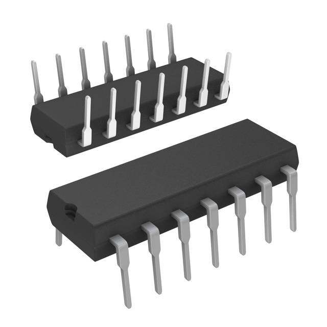
| 描述 | IC POT DGTL DUAL 128POS 14-SOIC数字电位计 IC IC 7-BIT Rw/ UP/DWN CONTROL |
| DevelopmentKit | EVAL-AD5222SDZ |
| 产品分类 | |
| 品牌 | Analog Devices Inc |
| 产品手册 | |
| 产品图片 |
|
| rohs | 符合RoHS无铅 / 符合限制有害物质指令(RoHS)规范要求 |
| 产品系列 | 数字电位计 IC,Analog Devices AD5222BRZ10- |
| 数据手册 | |
| 产品型号 | AD5222BRZ10 |
| POT数量 | Dual |
| 产品种类 | 数字电位计 IC |
| 供应商器件封装 | 14-SOICN |
| 包装 | 管件 |
| 商标 | Analog Devices |
| 存储器类型 | 易失 |
| 安装类型 | 表面贴装 |
| 安装风格 | SMD/SMT |
| 容差 | 30 % |
| 封装 | Tube |
| 封装/外壳 | 14-SOIC(0.154",3.90mm 宽) |
| 封装/箱体 | SOIC-14 |
| 工作温度 | -40°C ~ 85°C |
| 工作电源电压 | 2.7 V |
| 工厂包装数量 | 56 |
| 弧刷存储器 | Volatile |
| 抽头 | 128 |
| 接口 | 4 线串行(芯片选择,递增,增/减) |
| 数字接口 | Up/Down |
| 最大工作温度 | + 85 C |
| 最小工作温度 | - 40 C |
| 标准包装 | 56 |
| 每POT分接头 | 128 |
| 温度系数 | 标准值 -35 ppm/°C |
| 电压-电源 | 2.7 V ~ 5.5 V, ±2.3 V ~ 2.7 V |
| 电源电压-最大 | 5.5 V |
| 电源电压-最小 | 2.7 V |
| 电源电流 | 15 uA |
| 电路数 | 2 |
| 电阻 | 10 kOhms |
| 电阻(Ω) | 10k |
| 系列 | AD5222 |
| 缓冲刷 | Buffered |


- 商务部:美国ITC正式对集成电路等产品启动337调查
- 曝三星4nm工艺存在良率问题 高通将骁龙8 Gen1或转产台积电
- 太阳诱电将投资9.5亿元在常州建新厂生产MLCC 预计2023年完工
- 英特尔发布欧洲新工厂建设计划 深化IDM 2.0 战略
- 台积电先进制程称霸业界 有大客户加持明年业绩稳了
- 达到5530亿美元!SIA预计今年全球半导体销售额将创下新高
- 英特尔拟将自动驾驶子公司Mobileye上市 估值或超500亿美元
- 三星加码芯片和SET,合并消费电子和移动部门,撤换高东真等 CEO
- 三星电子宣布重大人事变动 还合并消费电子和移动部门
- 海关总署:前11个月进口集成电路产品价值2.52万亿元 增长14.8%


PDF Datasheet 数据手册内容提取
a Increment/Decrement Dual Digital Potentiometer AD5222 FEATURES FUNCTIONAL BLOCK DIAGRAM 128-Position, 2-Channel Potentiometer Replacement 10kV, 50kV, 100kV, 1MV VDD AD5222 A1 Very Low Power: 40 mA Max UP/DOWN 62.7 V Dual Supply Operation or U/D COUNTER DECODE W1 2.7 V to 5.5 V Single Supply Operation B1 Increment/Decrement Count Control POR APPLICATIONS A2 Stereo Channel Audio Level Control CS DAC Mechanical Potentiometer Replacement DAMCOSDEEL SEALNEDCT CUOP/UDNOTWENR DECODE W2 ENABLE Remote Incremental Adjustment Applications CLK B2 Instrumentation: Gain, Offset Adjustment GND VSS Programmable Voltage-to-Current Conversion Line Impedance Matching GENERAL DESCRIPTION mechanical or push-button switches (or other contact closure The AD5222 provides a dual channel, 128-position, digitally devices). This simple digital interface eliminates the need for controlled variable-resistor (VR) device. This device performs microcontrollers in front panel interface designs. the same electronic adjustment function as a potentiometer or The AD5222 is available in the surface-mount (SO-14) package. variable resistor. These products were optimized for instrument For ultracompact solutions, selected models are available in the and test equipment push-button applications. Choices between thin TSSOP-14 package. All parts are guaranteed to operate bandwidth or power dissipation are available as a result of the over the extended industrial temperature range of –40(cid:176) C to wide selection of end-to-end terminal resistance values. +85(cid:176) C. For 3-wire, SPI-compatible interface applications, see The AD5222 contains two fixed resistors with wiper contacts that the AD5203/AD5204/AD5206, AD7376, and AD8400/AD8402/ tap the fixed resistor value at a point determined by a digitally AD8403 products. controlled up/down counter. The resistance between the wiper and either end point of the fixed resistor provides a constant 5V resistance step size that is equal to the end-to-end resistance VDD divided by the number of positions (e.g., R = 10kW /128 = STEP A1 78W ). The variable resistor offers a true adjustable value of CS resistance, between Terminal A and the wiper, or TerminalB U/D U/D W1 and the wiper. The fixed A-to-B terminal resistance of 10kW , CLK B1 50kW , 100kW , or 1MW has a nominal temperature coefficient INCREMENT of –35 ppm/(cid:176) C. The chip select CS, count CLK and U/D direction control inputs A2 set the variable resistor position. The MODE determines whether DACSEL W2 both VRs are incremented together or independently. With MODE B2 MODE at logic zero, both wipers are incremented UP or DOWN without changing the relative settings between the wipers. Also, GND VSS the relative ratio between the wipers is preserved if either wiper reaches the end of the resistor array. In the independent MODE Figure 1.Typical Push-Button Control Application (Logic1) only the VR determined by the DACSEL pin is changed. DACSEL (Logic 0) changes RDAC 1. These inputs, which con- trol the internal up/down counter, can be easily generated with REV.0 Information furnished by Analog Devices is believed to be accurate and reliable. However, no responsibility is assumed by Analog Devices for its use, nor for any infringements of patents or other rights of third parties One Technology Way, P.O. Box 9106, Norwood, MA 02062-9106, U.S.A. which may result from its use. No license is granted by implication or Tel: 781/329-4700 World Wide Web Site: http://www.analog.com otherwise under any patent or patent rights of Analog Devices. Fax: 781/326-8703 © Analog Devices, Inc., 1999
AD5222–SPECIFICATIONS (V = 3 V 6 10% or 5 V 6 10%, V = 0 V, V = +V , V = 0 V, –408C < T < +858C, DD SS A DD B A unless otherwise noted.) Parameter Symbol Condition Min Typ1 Max Unit DC CHARACTERISTICS RHEOSTAT MODE (Specifications Apply to All VRs) Resistor Differential NL2 R-DNL R , V = NC –1 – 1/4 +1 LSB WB A Resistor Nonlinearity2 R-INL R , V = NC –1 – 0.4 +1 LSB WB A Nominal Resistor Tolerance D R V = V , Wiper = No Connect, T = 25(cid:176) C –30 +30 % AB DD A Resistance Temperature Coefficient R /D T V = V , Wiper = No Connect –35 ppm/(cid:176)C AB AB DD Wiper Resistance3 R I = V /R, V = 3 V or 5 V 45 100 W W W DD DD Nominal Resistance Match D R/R CH 1 to 2, V = V , T = 25(cid:176) C 0.2 1 % O AB DD A DC CHARACTERISTICS POTENTIOMETER DIVIDER MODE (Specifications Apply to All VRs) Resolution N 7 Bits Integral Nonlinearity4 INL R = 10 kW , 50 kW , or 100 kW –1 – 1/4 +1 LSB AB INL R = 1 MW –2 – 1/2 +2 LSB AB Differential Nonlinearity4 DNL –1 – 1/4 +1 LSB Voltage Divider Temperature Coefficient D V /D T Code = 40 20 ppm/(cid:176)C W H Full-Scale Error V Code = 7F –1 –0.5 +0 LSB WFSE H Zero-Scale Error V Code = 00 0 0.5 1 LSB WZSE H RESISTOR TERMINALS Voltage Range5 V V V V A, B, W SS DD Capacitance6 A, B C f = 1 MHz, Measured to GND, Code = 40 45 pF A, B H Capacitance6 W C f = 1 MHz, Measured to GND, Code = 40 60 pF W H Common-Mode Leakage I V = V = V 1 nA CM A B W DIGITAL INPUTS AND OUTPUTS Input Logic High V V = 5 V/3 V 2.4/2.1 V IH DD Input Logic Low V V = 5 V/3 V 0.8/0.6 V IL DD Input Current I V = 0 V or 5 V – 1 m A IL IN Input Capacitance6 C 5 pF IL POWER SUPPLIES Power Single-Supply Range V V = 0 V 2.7 5.5 V DD RANGE SS Power Dual-Supply Range V – 2.3 – 2.7 V DD/SS RANGE Positive Supply Current I V = 5 V or V = 0 V 15 40 m A DD IH IL Negative Supply Current I V = –2.5 V, V = +2.7 V 15 40 m A SS SS DD Power Dissipation7 P V = 5 V or V = 0 V, V = 5 V 150 400 m W DISS IH IL DD Power Supply Sensitivity PSS 0.002 0.05 %/% DYNAMIC CHARACTERISTICS6, 8, 9 Bandwidth –3 dB BW_10K R = 10 kW , Code = 40 1000 kHz AB H BW_50K R = 50 kW , Code = 40 180 kHz AB H BW_100K R = 100 kW , Code = 40 78 kHz AB H BW_1M R = 500 kW , Code = 40 7 kHz AB H Total Harmonic Distortion THD V = 1 V rms + 2 V dc, V = 2 V dc, f = 1 kHz 0.005 % W A B V Settling Time t R = 10 kW , – 1 LSB Error Band 2 m s W S AB Resistor Noise Voltage e R = 5 kW , f = 1 kHz 14 nV(cid:214) Hz N_WB WB INTERFACE TIMING CHARACTERISTICS (Applies to All Parts)6, 10 Input Clock Pulsewidth t , t Clock Level High or Low 30 ns CH CL CS to CLK Setup Time t 20 ns CSS CS Rise to CLK Hold Time t 20 ns CSH U/D to Clock Fall Setup Time t 10 ns UDS U/D to Clock Fall Hold Time t 30 ns UDH DACSEL to Clock Fall Setup Time t 20 ns DSS DACSEL to Clock Fall Hold Time t 30 ns DSH MODE to Clock Fall Setup Time t 20 ns MDS MODE to Clock Fall Hold Time t 40 ns MDH NOTES 1Typicals represent average readings at 25(cid:176)C, V = 5 V. DD 2Resistor position nonlinearity error R-INL is the deviation from an ideal value measured between the maximum resistance and the minimum resistance wiper positions. R-DNL measures the relative step change from ideal between successive tap positions. Parts are guaranteed monotonic. See Figure 22 test circuit. 3Wiper resistance is not measured on the R = 1 MW models. AB 4INL and DNL are measured at V with the RDAC configured as a potentiometer divider similar to a voltage output D/A converter. V = V and V = 0V. DNL W A DD B specification limits of – 1 LSB maximum are guaranteed monotonic operating conditions. See Figure 21 test circuit. 5Resistor Terminals A, B, W have no limitations on polarity with respect to each other. 6Guaranteed by design and not subject to production test. 7P is calculated from (I · V ). CMOS logic level inputs result in minimum power dissipation. DISS DD DD 8Bandwidth, noise and settling time are dependent on the terminal resistance value chosen. The lowest R value results in the fastest settling time and highest bandwidth. The highest R value results in the minimum overall power consumption. 9All dynamic characteristics use V = 5 V. DD 10See timing diagram for location of measured values. All input control voltages are specified with t = t = 2.5 ns (10% to 90% of +3 V) and timed from a voltage level R F of 1.5 V. Switching characteristics are measured using both V = 5 V or V = 3 V. DD DD Specifications subject to change without notice. –2– REV. 0
AD5222 ABSOLUTE MAXIMUM RATINGS ORDERING GUIDE (T = 25(cid:176)C, unless otherwise noted) A V to GND . . . . . . . . . . . . . . . . . . . . . . . . . . . . –0.3 V, +7 V Kilo Package Package DD V to GND . . . . . . . . . . . . . . . . . . . . . . . . . . . . . . . 0 V, –5 V Model Ohms Temperature Description Option SS V to V . . . . . . . . . . . . . . . . . . . . . . . . . . . . . . . . . . . . . 7 V DD SS AD5222BR10 10 –40(cid:176) C/+85(cid:176) C SO-14 R-14 V , V , V to GND . . . . . . . . . . . . . . . . . . . . . . . . . . 0 V, V A B W DD AD5222BRU10 10 –40(cid:176) C/+85(cid:176) C TSSOP-14 RU-14 A – B , A – W , B – W . . . . . . . . . . . . . . . . . . . – 20 mA X X X X X X AD5222BR50 50 –40(cid:176) C/+85(cid:176) C SO-14 R-14 Digital Input Voltage to GND . . . . . . . . . . . . 0 V, V + 0.3 V DD AD5222BRU50 50 –40(cid:176) C/+85(cid:176) C TSSOP-14 RU-14 Operating Temperature Range . . . . . . . . . . . –40(cid:176) C to +85(cid:176) C AD5222BR100 100 –40(cid:176) C/+85(cid:176) C SO-14 R-14 Maximum Junction Temperature (T max) . . . . . . . . . . 150(cid:176) C J AD5222BRU100 100 –40(cid:176) C/+85(cid:176) C TSSOP-14 RU-14 Storage Temperature . . . . . . . . . . . . . . . . . . –65(cid:176) C to +150(cid:176) C AD5222BR1M 1,000 –40(cid:176) C/+85(cid:176) C SO-14 R-14 Lead Temperature (Soldering, 10 sec) . . . . . . . . . . . . . 300(cid:176) C AD5222BRU1M 1,000 –40(cid:176) C/+85(cid:176) C TSSOP-14 RU-14 Package Power Dissipation . . . . . . . . . . . . . (T max – T )/q J A JA Thermal Resistance q , The AD5222 die size is 56 mil · 60 mil, 3360 sq. mil; 1.4224 mm · 1.524 mm, JA SOIC (SO-14) . . . . . . . . . . . . . . . . . . . . . . . . . . . . 158(cid:176) C/W 2.1677 sq. mm. Contains 1503 transistors. Patent Number 5495245 applies. TSSOP-14 . . . . . . . . . . . . . . . . . . . . . . . . . . . . . . . 206(cid:176) C/W PIN FUNCTION DESCRIPTIONS Pin Name Description CS tCSS t tCH tCSH 1 B1 B Terminal RDAC #1. CL 2 A1 A Terminal RDAC #1. CLK t 3 W1 Wiper RDAC #1, DACSEL = 0. UDS 4 V Negative Power Supply. Specified for operation SS U/D tUDH at both 0 V or –2.7 V (Sum of |V | + |V | DD SS tDSS < 5.5 V). 5 W2 Wiper RDAC #2, DACSEL = 1. DACSEL tDSH 6 A2 A Terminal RDAC #2. t MDS 7 B2 B Terminal RDAC #2. MODE tMDH 8 GND Ground. Figure 2. Detail Timing Diagram 9 MODE Common MODE = 0, Independent MODE = 1. 10 DACSEL DAC Select determines which wiper is incre- Truth Table mented in the Independent MODE = 1. DACSEL = 0 sets RDAC1, DACSEL = 1 sets CS CLK U/D Operation RDAC2. L t H Wiper Increment Toward Terminal A 11 U/D UP/DOWN Direction Control. L t L Wiper Decrement Toward Terminal B 12 CLK Serial Clock Input, Negative Edge Triggered. H X X Wiper Position Fixed 13 CS Chip Select Input, Active Low. When CS is high, the UP/DOWN counter is disabled. Common Mode (MODE = 0) moves both wipers together either 14 V Positive Power Supply. Specified for operation UP or DOWN the resistor array without changing the relative DD at both +3 V or +5 V. (Sum of |V | + |V | distance between the wipers. Also, the distance between both DD SS < 5.5 V). wipers is preserved if either reaches the end of the array. Inde- pendent Mode (MODE = 1) allows user to control each RDAC individually: DACSEL = 0 sets RDAC1; DACSEL = 1: sets PIN CONFIGURATION RDAC2. B1 1 14 VDD A1 2 13 CS W1 3 AD5222 12 CLK TOP VIEW VSS 4 (Not to Scale)11U/D W2 5 10 DACSEL A2 6 9 MODE B2 7 8 GND CAUTION ESD (electrostatic discharge) sensitive device. Electrostatic charges as high as 4000V readily WARNING! accumulate on the human body and test equipment and can discharge without detection. Although the AD5222 features proprietary ESD protection circuitry, permanent damage may occur on devices subjected to high energy electrostatic discharges. Therefore, proper ESD precautions are ESD SENSITIVE DEVICE recommended to avoid performance degradation or loss of functionality. REV. 0 –3–
AD5222–Typical Performance Characteristics 100 0.25 0.20 RAB75 0.15 TA = –558C % B 0.10 TA = +258C NOMINALTANCE – 50 ROR – LS 0.050 PERCENT OF ND-TO-END RESIS 25 R-DNL ER–––000...011055 TA = +858C VVDSSD == –+1155VV E RWB RWA –0.20 RAB = 50kV 0 –0.25 0 32 64 96 128 0 16 32 48 64 80 96 112 128 CODE – Decimal CODE – Decimal Figure 3.Wiper-To-End Terminal Resistance vs. Code Figure 6.R-DNL Relative Resistance Step Position Change vs. Code 5 1.0 3FH VDD/VSS = 2.7V/0V 4.5 20H 0.8 TA = 258C 4 10H 0.6 LTAGE – V23..553 08H 05H ROR – LSB 00..240 50kV VERSION 10kV VERSION O R V E V WB1.52 02H R-INL ––00..24 100kV VERSION 1MV VERSION 1 RAB = 10kV –0.6 VDD = 5V 0.5 TA = 258C –0.8 0 –1.0 0 1 2 3 4 5 6 7 0 16 32 48 64 80 96 112 128 IWA CURRENT – mA CODE – Decimal Figure 4.Resistance Linearity vs. Conduction Current Figure 7.R-INL Resistance Nonlinearity Error vs. Code 180 0.6 SS = 600 UNITS VDD/VSS = 2.7V/0V VDD = 2.7V 0.4 TA = 258C 150 TA = 258C 0.2 10kV VERSION 50kV VERSION 120 EQUENCY 90 L – LSB –0.20 R N F 60 I –0.4 100kV VERSION –0.6 30 1MV VERSION –0.8 0 40 41 42 44 45 47 48 50 51 53 54 56 57 59 60 –1.0 WIPER RESISTANCE – V 0 16 32 48 64 80 96 112 128 CODE – Decimal Figure 5.Wiper Contact Resistance Figure 8.Potentiometer Divider INL Error vs. Code –4– REV. 0
AD5222 70 9 VDD = +2.7V 8PCO – ppm/C 546000 1MV1 V0kE1VR0 S0VkIEOVRN SVIEORNSION VTAD D=/ V2S5S8C = 2.7V/0V 036 DVVVSABAS T== A= 50 –0V=2m 4.7V0VH rms 10kV M MODE TE 3200 50kV VERSION AIN – dB ––63 A W OP42 1MV 50kV R 10 G –9 E MET 0 –12 B NTIO–10 –15 BW10kV 764kHz 100kV TE 50kV 132kHz PO–20 –18 11M00VkV 66.46kkHHzz –30 –21 0 16 32 48 64 80 96 112 128 100 1k 10k 100k 1M CODE – Decimal FREQUENCY – Hz Figure 9. DV /DT Potentiometer Mode Tempco Figure 12.Gain vs. Frequency vs. R WB AB 10 120 FILTER = 22kHz 100 VDD/VSS = 2.7V/0V VDD = 62.7V 8m/C 80 100kV VERSION TA = 258C TVAIN = = 2 15V8C rms p 1.0 p CO – 60 50kV VERSION – % P 40 E M S MODE TE 200 HD + NOI0.1 SEE TEST CIRCUIT FIGURE 25 T T A –20 OST 10kV VERSION 0.01 SEE TEST CIRCUIT FIGURE 26 E –40 H R –60 1MV VERSION –80 0.001 0 16 32 48 64 80 96 112 128 10 100 1k 10k 100k CODE – Decimal FREQUENCY – Hz Figure 10. DR /DT Rheostat Mode Tempco Figure 13.Total Harmonic Distortion Plus Noise vs. WB Frequency 0 CODE = 3FH V 20H B/DI 1MV 100kV 10kV –10 1d 0. GAIN - dB––3200 100084HHH AIN FLATNESS – SVVVDVEDSABASD ET== A= =T50 E–0V2=2mS. 74.T7VV0 VH CrmIRsUIT 27 50kV 02H D G A 01H LIZE W OP42 –40 MA R TA = 258C NO B SEE TEST CIRCUIT FIGURE 32 –50 10 100 1k 10k 100k 1M 10M 10 100 1k 10k 100k 1M FREQUENCY – Hz FREQUENCY – Hz Figure 11.10 kW Gain vs. Frequency vs. Code Figure 14.Normalized Gain Flatness vs. Frequency REV. 0 –5–
AD5222 1200 10 A – VDD = 5.5V TA = 258C CODE = 15H 1000 B – VDD = 3.3V VDD = 5.5V m– A C – V CDOD D=E 5 .=5 V15H A 1 VA = 5.5V – SUPPLY CURRENT 864000000 D – V CCDOOD DD=EE 3 ==.3 V33FFHH A B UPPLY CURRENT – m 0.1 VVDAD =/ V2S.5SV = 62.5V D S 0.01 D I 200 C VDD = 2.7V 0 D 0.001 VA = 2.7V 1 10k 100k 1M 10M 0 1 2 3 4 5 6 FREQUENCY – Hz INPUT LOGIC VOLTAGE – V Figure 15.I , I Supply Current vs. Clock Frequency Figure 18.Supply Current vs. Input Logic Voltage DD SS 100 TA = 258C 90 VE – 8700 VDD/VSS = 2.7V/0V VVVDABD == =20 .V27.V7V VW NC 20mV/DIV A T 60 S SI RE 50 CH VDD/VSS = 62.7V T 40 WI 2V/DIV S 30 VDD/VSS = 5.5V/0V CLK 20 10 –3 –2 –1 0 1 2 3 4 5 6 COMMON MODE – Volts Figure 16.Incremental Wiper Contact Resistance vs. Figure 19.Midscale Transition 3F to 40 H H V /V DD SS 1 LOGIC = 0V OR VDD VDD = 2.7V VWA A VA = 2.7V T – m 0.1 VB = 0V VWB EN 20mV/DIV R CUR VDD = 5.5V OR VDD/VSS = 62.7V PLY 0.01 VDD = 2.7V P U CLK S 2V/DIV 0.001 –40 –15 10 35 60 85 TEMPERATURE – 8C Figure 17.Supply Current vs. Temperature Figure 20.Stereo Step Transition, Mode = 0 –6– REV. 0
Parametric Test Circuits–AD5222 A DUT B DUT V+ = VDD W +5V A 1LSB = V+/128 VIN W V+ OP279 VOUT B + VMS –5V Figure 21. Potentiometer Divider Nonlinearity Error Test Figure 25.Inverting Programmable Gain Test Circuit Circuit (INL, DNL) +5V NO CONNECT DUT IW VIN W OP279 VOUT A W –5V B A DUT B VMS Figure 22.Resistor Position Nonlinearity Error (Rheostat Figure 26.Noninverting Programmable Gain Test Circuit Operation; R-INL, R-DNL) +15V A DUT IW = VDD/RNOMINAL W VMS2 A W VW VIN DUT B OP42 VOUT B VMS1 RW = [VMS1 – VMS2]/IW –15V Figure 23.Wiper Resistance Test Circuit Figure 27.Gain vs. Frequency Test Circuit VA DUT RSW = 0IS.1WV V+ ~ VDD AB W VMS VPP+SS RS= RV(% D(dD/%B ±)) 1==0 2–%DD0–VV –LMD–O–DSG–%%– ( D–D–VV–MD–SD– ) B W ISW CODE = 00H 0.1V 0 TO VDD Figure 24.Power Supply Sensitivity Test Circuit (PSS, Figure 28.Incremental ON Resistance Test Circuit PSRR) REV. 0 –7–
AD5222 OPERATION U/D The AD5222 provides a 128-position, digitally-controlled, variable resistor (VR) device. Changing the VR settings is accomplished by pulsing the CLK pin while CS is active low. The U/D (UP/ DACSEL RDAC 1 DOWN) control input pin controls the direction of the increment. U/D COUNTER When the wiper hits the end of the resistor (Terminal A or B) additional CLK pulses no longer change the wiper setting. The wiper position is immediately decoded by the wiper decode logic MODE changing the wiper resistance. Appropriate debounce circuitry is required when push-button switches are used to control the count sequence and direction of count. The exact timing require- ments are shown in Figure 2. The AD5222 powers ON in a centered wiper position, exhibiting nearly equal resistances of RDAC 2 CS U/D R and R . WA WB COUNTER CLK VDD AD5222 A1 Figure 30.Detailed Digital Logic Interface Circuit UP/DOWN U/D COUNTER DECODE W1 All digital inputs (CS, U/D, CLK, MODE, DACSEL) are B1 protected with a series input resistor and parallel Zener ESD structure shown in Figure 31. All potentiometer terminal pins POR (A, B, W) are protected from ESD as shown in Figure 32. A2 CS DAC DAMCOSDEEL SEALNEDCT CUOP/UDNOTWENR DECODE W2 1kV ENABLE LOGIC CLK B2 VSS GND VSS Figure 31.Equivalent ESD Protection Digital Pins Figure 29.Block Diagram 20V A, B, W DIGITAL INTERFACING OPERATION The AD5222 contains a push-button controllable interface. The VSS active inputs are clock (CLK), CS and up/down (U/D). While Figure 32.Equivalent ESD Protection Analog Pins the MODE, and DACSEL pins control common updates or individual updates. The negative-edge sensitive CLK input A requires clean transitions to avoid clocking multiple pulses into RS the internal UP/DOWN counter register, Figure 30. Standard logic families work well. If mechanical switches are used for D0 RS product evaluation a flip-flop or other suitable means should D1 debounce them. When CS is taken active low, the clock begins D2 to increment or decrement the internal up/down counter, depen- D3 RS D4 dent upon the state of the U/D control pin. The UP/DOWN D5 D6 counter value (D) starts at 40 at system power ON. Each new H W CLK pulse will increment the value of the internal counter by RDAC 1LSB until the full-scale value of 7F is reached, as long as the UP/DOWN H CNTR U/D pin is logic high. If the U/D pin is taken to logic low, the & counter will count down, stopping at code 00 (zero-scale). DECODE H Additional clock pulses on the CLK pin are ignored when the wiper is at either the 00 position or the 7F position. The H H RS detailed digital logic interface circuitry is shown in Figure 30. B RS = RNOMINAL/128 Figure 33.AD5222 Equivalent RDAC Circuit –8– REV. 0
AD5222 PROGRAMMING THE VARIABLE RESISTOR The R temperature coefficient increases as the wiper is pro- BA Rheostat Operation grammed near the B-terminal due to the larger percentage The nominal resistance of the RDAC between Terminals A and contribution of the wiper contact switch resistance, which has a B are available with values of 10kW , 50kW , 100kW , and 1MW 0.5%/(cid:176) C temperature coefficient. Figures 9 and 10 show the The final three characters of the part number determine the effect of the wiper contact resistance as a function of code setting. nominal resistance value, e.g., 10kW = 10; 50kW = 50; 100kW = 100; 1 MW = 1M. The nominal resistance (R ) of the VR PROGRAMMING THE POTENTIOMETER DIVIDER AB has 128 contact points accessed by the wiper terminal, plus the Voltage Output Operation B terminal contact. At power ON, the resistance from the wiper The digital potentiometer easily generates an output voltage to either end Terminal A or B is approximately equal. Pulsing proportional to the input voltage applied to a given terminal. the CLK pin will increase the resistance from the wiper W to For example connecting A-terminal to 5V and B-terminal to Terminal B by one unit of R resistance, see Figure 33. The ground produces an output voltage at the wiper which can be S resistance R is determined by the number of pulses applied to any value starting at zero volts up to 1 LSB less than 5V. Each WB the clock pin. Each segment of the internal resistor string has a LSB of voltage is equal to the voltage applied across Terminals nominal resistance value of R = R /128, which becomes 78W AB divided by the 128-position resolution of the potentiometer S AB in the case of the 10kW AD5222BR10 product. Care should be divider. The general equation defining the output voltage with taken to limit the current flow between W and B in the direct respect to ground for any given input voltage applied to Termi- contact state (R code = 0) to a maximum value of 20mA to nals AB is: WB avoid degradation or possible destruction of the internal switch V (D) = D/128 · V + V (1) contact. W AB B D represents the current contents of the internal up/down counter. Like the mechanical potentiometer the RDAC replaces, it is totally symmetrical (see Figure 3). The resistance between the Operation of the digital potentiometer in the divider mode wiper W and Terminal A also produces a digitally controlled results in more accurate operation over temperature. Here the resistance R . When these terminals are used the B-terminal output voltage is dependent on the ratio of the internal resistors WA not the absolute value, therefore, the drift improves to 20ppm/(cid:176) C. should be tied to the wiper. The typical part-to-part distribution of R is process-lot- BA dependent having a – 30% variation. The change in R with BA temperature has a –35 ppm/(cid:176) C temperature coefficient. REV. 0 –9–
AD5222 OUTLINE DIMENSIONS Dimensions shown in inches and (mm). 14-Lead Narrow Body SOIC 14-Lead TSSOP (R-14) (RU-14) 9 0.3444 (8.75) 0.201 (5.10) 9 0.3367 (8.55) 0.193 (4.90) 10/ – 8 – 0.1574 (4.00) 14 8 0.2440 (6.20) 14 8 15 0.1497 (3.80) 1 7 0.2284 (5.80) 00..117679 ((44..5300)) C37 0.256 (6.50) PIN 1 0.05B0S (C1.27) 00..00658382 ((11..7355)) 00..00109969 ((00..5205))3 458 1 7 0.246 (6.25) PIN 1 88 00..00009480 ((00..2150)) 00..00119328 ((00..4395)) SPELAANTIENG 00..00009795 ((00..2159))08 00..00510600 ((10..2471)) 00..000062 ((00..1055)) 0.04M33A (X1.10) 88 SEPALTAINNGE 0(B.00.S26C556) 00..00101785 ((00..3109)) 00.0.0003759 ( (00.0.2900))08 00..002280 ((00..7500)) A. S. U. N D I E T N RI P –10– REV. 0