ICGOO在线商城 > 隔离器 > 光隔离器 - 逻辑输出 > ACNV2601-000E
/ACNV2601-000E.jpg)
 Datasheet下载
- 型号: ACNV2601-000E
- 制造商: Avago Technologies
- 库位|库存: xxxx|xxxx
- 要求:
| 数量阶梯 | 香港交货 | 国内含税 |
| +xxxx | $xxxx | ¥xxxx |
查看当月历史价格
查看今年历史价格
ACNV2601-000E产品简介:
ICGOO电子元器件商城为您提供ACNV2601-000E由Avago Technologies设计生产,在icgoo商城现货销售,并且可以通过原厂、代理商等渠道进行代购。 ACNV2601-000E价格参考。Avago TechnologiesACNV2601-000E封装/规格:光隔离器 - 逻辑输出, Logic Output Optoisolator 10MBd Open Collector, Schottky Clamped 7500Vrms 1 Channel 20kV/µs CMTI 10-DIP。您可以下载ACNV2601-000E参考资料、Datasheet数据手册功能说明书,资料中有ACNV2601-000E 详细功能的应用电路图电压和使用方法及教程。
Broadcom Limited的光隔离器型号ACNV2601-000E(逻辑输出)主要应用于需要电气隔离和信号传输的场景。以下为其具体应用场景:

 1. 工业自动化
   - 在工业控制中,用于隔离传感器、执行器与控制系统之间的信号,防止高电压或噪声干扰。
   - 常见于可编程逻辑控制器(PLC)、数据采集系统和电机驱动器中。

 2. 医疗设备
   - 用于医疗监测设备(如心电图仪、血压计等),确保患者与设备之间的安全隔离,避免电流泄漏。
   - 提供稳定的信号传输,保证测量精度。

 3. 通信系统
   - 在电信设备中,用于隔离电源和信号线路,防止电磁干扰(EMI)和地环路问题。
   - 应用于光纤通信接口、网络交换机和路由器中。

 4. 汽车电子
   - 在车载电子系统中,用于隔离发动机控制单元(ECU)与其他模块的信号,提高系统的抗干扰能力。
   - 适用于电动汽车中的电池管理系统(BMS),保护敏感电路免受高压影响。

 5. 电力系统
   - 在智能电网和电力监控系统中,用于隔离高压环境下的信号传输,确保数据的准确性和安全性。
   - 应用于继电器控制、电表读取和电力保护装置中。

 6. 消费电子
   - 在家用电器(如洗衣机、空调等)中,用于隔离主控板与功率器件之间的信号,提高系统的可靠性和寿命。
   - 适用于音频设备和视频设备中的信号隔离。

 特点总结:
- 高隔离电压:提供强大的电气隔离能力,保护敏感电路。
- 快速响应:适合高速信号传输的应用。
- 低功耗:减少热量产生,提高系统效率。
- 可靠性强:能够在恶劣环境下稳定工作。

该型号的光隔离器广泛应用于对安全性和稳定性要求较高的领域,是现代电子系统中不可或缺的关键组件之一。
| 参数 | 数值 |
| 产品目录 | |
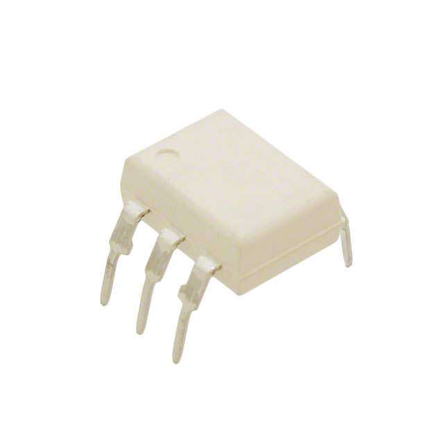
| 描述 | OPTOCOUPLER DGTL 10MBD 10DIP高速光耦合器 10MBd Optocoupler 2mm DTI |
| 产品分类 | |
| 品牌 | Avago Technologies |
| 产品手册 | http://www.avagotech.com/pages/en/optocouplers_plastic/plastic_digital_optocoupler/10_mbd_logic_gate/acnv2601-000e |
| 产品图片 |
|
| rohs | 符合RoHS无铅 / 符合限制有害物质指令(RoHS)规范要求 |
| 产品系列 | 光耦合器/光电耦合器,高速光耦合器,Avago Technologies ACNV2601-000E- |
| 数据手册 | http://www.avagotech.com/docs/AV02-2456EN |
| 产品型号 | ACNV2601-000E |
| PCN封装 | |
| 上升/下降时间(典型值) | 25ns, 10ns |
| 上升时间 | 25 ns |
| 下降时间 | 10 ns |
| 产品种类 | 高速光耦合器 |
| 传播延迟tpLH/tpHL(最大值) | 80ns, 80ns |
| 供应商器件封装 | 10-DIP |
| 共模瞬态抗扰度(最小值) | 20kV/µs |
| 其它名称 | 516-2887 |
| 包装 | 管件 |
| 商标 | Avago Technologies |
| 安装类型 | 通孔 |
| 封装 | Tube |
| 封装/外壳 | 10-DIP(0.433",11.01mm) |
| 封装/箱体 | DIP-10 |
| 工作温度 | -40°C ~ 105°C |
| 工厂包装数量 | 175 |
| 数据速率 | 10 MBd |
| 最大功率耗散 | 85 mW |
| 最大反向二极管电压 | 3 V |
| 最大工作温度 | + 105 C |
| 最大正向二极管电压 | 7 V |
| 最小工作温度 | - 40 C |
| 标准包装 | 175 |
| 正向电流 | 20 mA |
| 每芯片的通道数量 | 1 Channel |
| 电压-正向(Vf)(典型值) | 1.64V |
| 电压-电源 | 4.5 V ~ 5.5 V |
| 电压-隔离 | 7500Vrms |
| 电流-DC正向(If) | 20mA |
| 电流-输出/通道 | 50mA |
| 绝缘电压 | 7500 Vrms |
| 输入-输入侧1/输入侧2 | 1/0 |
| 输入类型 | AC/DC |
| 输出类型 | 开集,肖特基箝位 |
| 输出设备 | Photo IC |
| 通道数 | 1 |


- 商务部:美国ITC正式对集成电路等产品启动337调查
- 曝三星4nm工艺存在良率问题 高通将骁龙8 Gen1或转产台积电
- 太阳诱电将投资9.5亿元在常州建新厂生产MLCC 预计2023年完工
- 英特尔发布欧洲新工厂建设计划 深化IDM 2.0 战略
- 台积电先进制程称霸业界 有大客户加持明年业绩稳了
- 达到5530亿美元!SIA预计今年全球半导体销售额将创下新高
- 英特尔拟将自动驾驶子公司Mobileye上市 估值或超500亿美元
- 三星加码芯片和SET,合并消费电子和移动部门,撤换高东真等 CEO
- 三星电子宣布重大人事变动 还合并消费电子和移动部门
- 海关总署:前11个月进口集成电路产品价值2.52万亿元 增长14.8%
PDF Datasheet 数据手册内容提取
ACNV2601 High Insulation Voltage 10-MBd Digital Optocoupler Data Sheet Description Features The ACNV2601 is an optically coupled gate that combines an High voltage insulation with minimum 13-mm creepage AlGaAs light-emitting diode and an integrated photo detector and clearance housed in a widebody package. The distance-through- 20 kV/μs minimum common mode rejection (CMR) at insulation (DTI) between the emitting diode and V =1500V CM photo-detector is at 2 mm. The output of the detector IC is an High speed: 10 MBd typical open collector Schottky clamped transistor. The internal shield TTL compatible provides a guaranteed common mode transient immunity specification of 20 kV/μs at V = 1500V. Open collector output cm Guaranteed AC and DC performance over wide With creepage and clearance of greater than 13 mm, temperature: –40°C to +105°C ACNV2601 is designed to provide high isolation voltage Available in 10-pin widebody packages (7500V ). It can withstand a continuous high working rms voltage of 2262 V and a surge voltage of 12,000 V , Safety approval: peak peak meeting IEC60747-5-5, UL, and CSA standard for reinforced — Approval at 7500 Vrms for 1 minute per UL1577 insulation. ACNV2601 provides the high insulation voltage — CSA protection at a high data rate of 10 MBd. — IEC/EN/DIN EN 60747-5-5 with V = 2262 V iorm peak Applications High voltage insulation CAUTION It is advised that normal static precautions be Instrument input/output isolation taken in handling and assembly of this component to prevent damage and/or Line receivers degradation which may be induced by ESD. The Ground loop elimination components featured in this data sheet are not Isolation of high-speed logic systems to be used in military or aerospace applications Microprocessor system interfaces or environments Broadcom - 1 -
ACNV2601 Data Sheet Functional Diagram Truth Table (Positive Logic) LED ENABLE OUTPUT NC 1 10 Vcc On H L Anode 2 9 Ve Off H H Cathode 3 8 Vo On L H NC 4 7 GND SHIELD Off L H NC 5 6 NC On NC L Off NC H NOTE A 0.1-μF bypass capacitor must be connected between pins V and GND. CC Ordering Information ACNV2601 is UL recognized with 7500 V for 1 minute per UL1577. rms Option Part Number Package Surface Gull Wing Tape & UL 7500 Vrms/ IEC/EN/DIN EN Quantity Mount Reel 1 Minute Rating 60747-5-5 RoHS Compliant ACNV2601 -000E 500 mil X X 35 per tube -300E DIP-10 X X X X 35 per tube -500E X X X X X 500 per reel To order, choose a part number from the Part Number column and combine with the desired option from the Option column to form an order entry. Example 1: ACNV2601-500E to order product of 500 mil DIP-10 Widebody with Gull Wing Surface Mount package in Tape and Reel packaging with both UL 7500 V /1 min and IEC/EN/DIN EN 60747-5-5 Safety Approval in RoHS compliant. rms Option data sheets are available. Contact your Broadcom sales representative or authorized distributor for information. Schematic IF ICC VCC 2+ 10 IO VO 8 VF – GND 3 SHIELD 7 IE 9 VE NOTE Use of a 0.1-μF bypass capacitor connected between pins of 7 and 10 is recommended. Broadcom - 2 -
ACNV2601 Data Sheet Package Drawings 10-Pin Widebody (500 mils) DIP Package [13.71 ± 0.15] 0.540 ± 0.006 A NNNNNNNN Device Part Number [11.01 ± 0.15] YYWW 0.433 ± 0.006 Lead Free EEE Date Code Pin 1 Dot Lot ID [13.01 ± 0.15] 0.512 ± 0.006 [1.30] 0.05 [0.51] [11.01 ± 0.15] TYP 0.020 MIN 25]21 0.433 ± 0.006 5.0. [ [05..22057] 0] 0.1220] 0.154 [1.998]0.08 19 3.3. [[ [13.06] 0.514 [1.78 ± 0.15] [0.48 ± 0.08] 0.070 ± 0.006 [2.54] 0.019 ± 0.003 0.10 [0.25 +- 0 0 . 0. 0 5 8 ] TYP 5° TYP 0.010+-00.0.00023 Dimensions in Inches [Millimeters] 10-Pin Widebody (500 mils) DIP Package with Gull Wing Surface Mount Option 300 LAND PATTERN RECOMMENDATION [1.30 ± 0.15] [13.71 ± 0.15] 0.051 ± 0.006 0.540 ± 0.006 5]06 A 0.10.0 ± ± Device Part Number NNNNNNNN [11.01 ± 0.15] [16.35 ± 0.15] 29 90 Lead Free YYWW 0.433 ± 0.006 0.644 ± 0.006 [[2.2.20.09 ± 0.15] EEE Date Code 0.090 ± 0.006 Pin 1 Dot Lot ID [14.90 ± 0.15] [1.30] 0.587 ± 0.006 0.051 TYP [13.01 ± 0.15] 0.512 ± 0.006 [0.75 ± 0.15] [0.254 + 0 . 0 7 6 ] [05..22057]MAX 0.030 ± 0.006 0.010 -+-00.0.00.5001023 [1.78 ± 0.15] 0.070 ± 0.006 0[1.0.0309 ±± 00..1050]6 5° NO M Dimension in Inches [Millimeter] Broadcom - 3 -
ACNV2601 Data Sheet Solder Reflow Profile Recommended reflow condition as per JEDEC Standard, J-STD-020 (latest revision). Non-Halide Flux should be used. Insulation and Safety Related Specifications Parameter Symbol ACNV2601 Unit Conditions Minimum External Air Gap L(101) 13 mm Measured from input terminals to output terminals, (External Clearance) shortest distance through air. Minimum External L(102) 13 mm Measured from input terminals to output terminals, Tracking (External Creepage) shortest distance path along body. Minimum Internal Plastic Gap 2.0 mm Through insulation distance conductor to conductor, (Internal Clearance) usually the straight line distance thickness between the emitter and detector. Minimum Internal Tracking 4.6 mm Measured from input terminals to output terminals, along (Internal Creepage) internal cavity. Tracking Resistance CTI 200 V DIN IEC 112/VDE 0303 Part 1. (Comparative Tracking Index) Isolation Group IIIa Material Group (DIN VDE 0110, 1/89, Table 1). Broadcom - 4 -
ACNV2601 Data Sheet IEC/EN/DIN EN 60747-5-5 Insulation Characteristicsa Description Symbol Characteristic Unit Installation Classification per DIN VDE 0110/1.89, Table 1 For Rated Mains Voltage ≤ 600 V I – IV rms For Rated Mains Voltage ≤ 1000 V I – III rms Climatic Classification 55/105/21 Pollution Degree (DIN VDE 0110/1.89) 2 Maximum Working Insulation Voltage V 2262 V IORM peak Input to Output Test Voltage, Method ba VPR 4241 Vpeak V x 1.875 = V , 100% Production Test with t = 1 sec, Partial Discharge < 5 pC IORM PR m Input to Output Test Voltage, Method aa VPR 3619 Vpeak V x 1.6 = V , Type and Sample Test, t = 10 sec, Partial Discharge < 5 pC IORM PR m Highest Allowable Overvoltage (Transient Overvoltage t = 60 sec) V 12000 V ini IOTM peak Safety-Limiting Values — Maximum Values Allowed in the Event of a Failure Case Temperature T 150 °C S Input Currentb IS, INPUT 400 mA Output Powerb PS, OUTPUT 1 W Insulation Resistance at TS, VIO = 500V RS >109 Ω a. Refer to the optocoupler section of the Isolation and Control Components Designer’s Catalog, under Product Safety Regulations section, (IEC/EN/DIN EN 60747-5-5) for a detailed description of Method a and Method b partial discharge test profiles. b. Refer to the following figure for dependence of P and I on ambient temperature: S S 1100 ENT - IS1090000 PISS ( (mmAW)) R R 800 U T C 700 U NP 600 P, IS 500 R - 400 E W 300 O P T 200 U TP 100 U O 0 0 25 50 75 100 125 150 175 Ts - CASE TEMPERATURE - °C NOTE These optocouplers are suitable for safe electrical isolation only within the safety limit data. Maintenance of the safety data shall be ensured by means of protective circuits. Broadcom - 5 -
ACNV2601 Data Sheet Absolute Maximum Ratings Parameter Symbol Min. Max. Unit Storage Temperature T –55 125 °C S Operating Temperature T –40 105 °C A Average Input Current I — 20 mA F(AVG) Reverse Input Voltage V — 3 V R Input Power Dissipation P — 40 mW I Supply Voltage (1 Minute Maximum) V — 7 V CC Enable Input Voltage (Not to exceed V by more than 500 mV) V — V + 0.5 V CC E CC Enable Input Current I — 5 mA E Output Collector Current I — 50 mA O Output Collector Voltage V — 7 V O Output Collector Power Dissipation P — 85 mW O Lead Solder Temperature T — 245°C for 10 sec, LS up to seat plane Recommended Operating Conditions Parameter Symbol Min. Max. Unit Notes Input Current, Low Level I a 0 250 μA FL Input Current, High Level I b 9 16 mA c FH Power Supply Voltage V 4.5 5.5 V CC Low Level Enable Voltage V 0 0.8 V EL High Level Enable Voltage V 2.0 V V EH CC Operating Temperature T –40 105 °C A Fan Out (at R = 1 kΩ) N — 5 TTL Loads L Output Pull-up Resistor R 330 4k Ω L a. The off condition can also be guaranteed by ensuring that V 0.8V. FL b. The initial switching threshold is 8 mA or less. It is recommended that 9 mA to 16 mA be used for best performance and to permit at least a 20% LED degradation guardband. c. Peaking circuits may produce transient input currents up to 50-mA, 50-ns maximum pulse width, provided average current does not exceed 20 mA. Broadcom - 6 -
ACNV2601 Data Sheet Electrical Specifications (DC) Over recommended operating conditions unless otherwise specified. All typicals at V = 5V, T = 25°C. CC A Parameter Symbol Min. Typ. Max. Unit Test Conditions Fig. Notes High Level Output Current I — 5.5 100 μA V = 5.5V, V = 2.0V a OH CC E V = 5.5V, I = 250 μA O FL Input Threshold Current I — 3.5 8 mA V = 5.5V, V = 2.0V, 1, 2 a TH CC E V = 0.6V, I > 13 mA O OL Low Level Output Voltage V — 0.35 0.6 V V = 5.5V, V = 2.0V, 1, 2, a OL CC E I = 8 mA, I = 13 mA 3, 4 F OL(Sinking) High Level Supply Current I — 7.0 12 mA V = 0.5V V = 5.5 V, CCH E CC I = 0 mA — 6.5 — V = V F E CC Low Level Supply Current I — 9.0 13 mA V = 0.5V V = 5.5V, CCL E CC I = 10 mA — 8.5 — V = V F E CC High Level Enable Current I — –0.7 — mA V = 5.5V, V = 2.0V EH CC E Low Level Enable Current I — –0.9 — mA V = 5.5V, V = 0.5V EL CC E High Level Enable Voltage V 2.0 — — mA V = 5.5 V, V = 2.0V a EH CC E Low Level Enable Voltage V — — 0.8 mA V = 5.5V, V = 0.5V EL CC E Input Forward Voltage V 1.25 1.64 1.85 V T = 25°C I = 10 mA 5 F A F 1.2 — 2.05 Input Reverse Breakdown Voltage BV 5 — — V I = 100 μA, T = 25°C R R A Input Capacitance C — 60 — pF f = 1 MHz, V = 0V IN F Input Diode Temperature ΔV /ΔT — –1.9 — mV/°C I = 10 mA F A F Coefficient a. No external pull-up is required for a high logic state on the enable input. If the V pin is not used, tying V to V results in improved CM performance E E CC R Broadcom - 7 -
ACNV2601 Data Sheet Switching Specifications (AC) Over recommended temperature (T = –40°C to +105°C), V = 5V, I = 10 mA unless otherwise specified. All typicals are at T = A CC F A 25°C, V = 5V. CC Parameter Symbol Min. Typ. Max. Unit Test Conditions Fig. Notes Propagation Delay Time to High tPLH 30 50 80 ns TA = 25°C RL = 350Ω, 6, 7, 8 a, b Output Level 120 CL = 15 pF Propagation Delay Time to Low t 35 55 80 ns T = 25°C c, b PHL A Output Level 120 Pulse Width Distortion |t – t | — 5 40 ns R = 350Ω, C = 15 pF 6, 7, 8, 9 b PHL PLH L L Propagation Delay Skew t — 50 ns d, b psk Output Rise Time (10% to 90%) T — 25 — ns 10 b r Output Fall Time (10% to 90%) T — 10 — ns 10 b f Propagation Delay Time of Enable t — 30 — ns R = 350Ω, C = 15 pF, 11, 12 e ELH L L from VEH to VEL VEL = 0V, VEH = 3V Propagation Delay Time of Enable t — 20 — ns R = 350Ω, C = 15 pF, 11, 12 f EHL L L from VEL to VEH VEL = 0V, VEH = 3V Output High Level Common |CMH| 20 25 — kV/μs VCC = 5 V, IF = 0 mA, 13 g, h, b Mode Transient Immunity V = 2V, R = 350Ω, O(MIN) L T = 25°C, V = 1500V A CM Output Low Level Common Mode |CML| 20 25 — kV/μs VCC = 5V, IF = 10 mA, h, i, b Transient Immunity V = 0.8V, R = 350Ω, O(MAX) L T = 25°C, V = 1500V A CM a. The t propagation delay is measured from the 5 mA point on the falling edge of the input pulse to the 1.5V point on the rising edge of the output pulse. PLH b. No external pull-up is required for a high logic state on the enable input. If the V pin is not used, tying V to V results in improved CM performance. E E CC R c. The tPHL propagation delay is measured from the 5 mA point on the rising edge of the input pulse to the 1.5V point on the falling edge of the output pulse. d. t is equal to the worst-case difference in t and/or t that is seen between units at any given temperature and specified test conditions. PSK PHL PLH e. The t enable propagation delay is measured from the 1.5V point on the falling edge of the enable input pulse to the 1.5V point on the rising edge of the ELH output pulse. f. The t enable propagation delay is measured from the 1.5V point on the rising edge of the enable input pulse to the 1.5V point on the falling edge of the EHL output pulse. g. CM is the maximum tolerable rate of rise of the common mode voltage to ensure that the output remains in a high logic state (i.e., V > 2.0V). H O h. For sinusoidal voltages, (|dV |/dt) = πf V . CM max CM CM(p-p) i. CM is the maximum tolerable rate of fall of the common mode voltage to ensure that the output remains in a low logic state (i.e., V < 0.8V). L O Package Characteristics All typicals are at T = 25°C. A Parameter Symbol Min. Typ. Max. Unit Test Conditions Fig. Notes Input-Output Insulation VISO 7500 — — Vrms RH < 50% for 1 min., TA = 25°C a, b Input-Output Resistance RI-O 1012 — — Ω VI-O = 500V a Input-Output Capacitance C — 0.5 0.6 pF f = 1 MHz, T = 25°C a I-O A a. Device considered a two-terminal device: pins 1, 2, 3, 4 and 5 shorted together, and pins 6, 7, 8, 9 and 10 shorted together. b. In accordance with UL1577, each optocoupler is proof tested by applying an insulation test voltage ≥9000 V for one second (leakage detection current rms limit, I ≤ 5 μA). This test is performed before the 100% production test for partial discharge (Method b) shown in the IEC/EN/DIN EN 60747-5-5 Insulation I-O Characteristicsa table, if applicable. Broadcom - 8 -
ACNV2601 Data Sheet Figure1 Typical Output Voltage vs. Forward Input Voltage Current Figure2 Typical Input Threshold Current vs. Temperature 6 6 VCC = 5V mA 5 TA = 25°C T - 5 OLTAGE - V 4 RL = 350 (cid:58) LD CURREN 4 T V 3 HO 3 RL = 350 (cid:58), 1k (cid:58), 4k (cid:58) U S V - OUTPO 12 RRLL == 14kk (cid:58)(cid:58) I - INPUT THRETH12 VVCE C= = 0 5.6.0 V V 0 0 0 1 2 3 4 5 -60 -40 -20 0 20 40 60 80 100 120 IF - FORWARD INPUT VOLTAGE - mA TA - TEMPERATURE - °C Figure3 Typical Low Level Output Voltage vs. Temperature Figure4 Typical Low Level Output Current vs. Temperature 0.8 70 V 0.7 VCC = 5.5 V mA VCC = 5.5 V oltage - 0.6 VIFE = = 8 2..00 m VA RRENT - 60 VVEO L= = 2 0.0.6 V V utput V 00..45 I0 = 16 mA I0 = 13 mA PUT CU 50 IF = 14-16 mA V - Low Level OOL000...123 I0 = 9.6 mA I0 = 6.4 mA - LOW LEVEL OUTOL 3400 IF = 10 mA IF = 8 mA 0 I 20 -60 -40 -20 0 20 40 60 80 100 120 -60 -40 -20 0 20 40 60 80 100 120 TA - TEMPERATURE - °C TA - TEMPERATURE - °C Figure5 Typical Input Diode Forward Characteristic 1000.000 100.000 A m T - 10.000 N E R R CU 1.000 D R A W 0.100 R O F I - F 0.010 TA = 25°C 0.001 1.2 1.3 1.4 1.5 1.6 1.7 1.8 VF - FORWARD VOLTAGE - V Broadcom - 9 -
ACNV2601 Data Sheet Figure6 Test Circuit for t and t PHL PLH +5 V PULSE GEN. IF 1 10 ZO = 50(cid:58) 2 9 0B.Y1P(cid:80)AFSS RL * C L PISR AOPBPER AONXDIM STARTAELYY W 1I5R pINFG W CHAIPCAHC IINTACLNUCDE.ES tf = tr = 5 ns OUTPUT VO IF = 10 mA 3 8 MONITORING INPUT INPUT *CL NODE IF IF = 5 mA MONITONROINDGE 4 SHIELD 7 tPHL tPLH RM 5 6 OUTPUT VO 1.5 V Figure7 Typical Propagation Delay vs. Temperature Figure8 Typical Propagation Delay vs. Pulse Input Current 100 90 90 VCC = 5.0 V tPLH, RL = 4k(cid:58) ns TA = 25°C tPLH, RL = 4k(cid:58) ns 80 Y - 80 Y - VCC = 5.0 V ELA 70 ELA 70 TA = 25°C D D GATION 60 tPLH, RL = 1k(cid:58) tPHL, RL = 350(cid:58) GATION 60 tPHL, RL = 350(cid:58) tPLH, RL =tP 1LkH(cid:58), RL = 350(cid:58) A 50 A P P 50 O O R R P 40 P t - p 30 tPLH, RL = 350(cid:58) (cid:3)t(cid:3)P(cid:3)H(cid:3)(cid:3)L(cid:3),(cid:3) (cid:3)R L = 41kk(cid:58)(cid:58) t - p 40 tPHL, RL = 1k(cid:58) tPHL, RL = 4k(cid:58) 20 30 -60 -40 -20 0 20 40 60 80 100 120 8 9 10 11 12 13 14 15 TA - TEMPERATURE - °C IF - PULSE INPUT CURRENT - mA Figure9 Typical Pulse Width Distortion vs. Temperature Figure10 Typical Rise and Fall Time vs. Temperature 40 300 ORTION - ns 233505 RL = 4k(cid:58) E - ns 220500 RL = 4k(cid:58) TH DIST 1250 VIFC =C = 1 05..00 mVA ALL TIM 150 VIFC =C = 1 05..00 mVA ttRFAISLEL D F WD - PULSE WI 1-0550 RL = 350(cid:58) RL = 1k(cid:58) t, t - RISE,rf15000 RL = 350(cid:58) RL = 1k(cid:58) RL = 350(cid:58), 1k(cid:58), 4k(cid:58) P -10 0 -60 -40 -20 0 20 40 60 80 100 120 -60 -40 -20 0 20 40 60 80 100 120 TA - TEMPERATURE - °C TA - TEMPERATURE - °C Broadcom - 10 -
ACNV2601 Data Sheet Figure11 Test Circuit for t and t EHL ELH PULSE GEN. ZO = 50(cid:58) tf = tr = 5 ns INPUT VE MONITORING NODE +5 V 1 10 10 mA 3.0 V IF 2 9 RL INPUT 3 8 0B.Y1P(cid:80)*ACFSLS MNOUOOTDNPEIUTOT RVION G VE tEHL tELH 1.5 V 4 7 OUTPUT SHIELD VO 1.5 V 5 6 *CL IS APPROXIMATELY 15 pF WHICH INCLUDES PROBE AND STRAY WIRING CAPACITANCE. Figure12 Typical Enable Propagation Delay vs. Temperature 100 Y - ns 80 VVCEHC == 53..00 VV DELA VIFE =L = 1 03..00 mVA tELH, RL = 4k(cid:58) N O 60 TI A G OPA 40 tELH, RL = 1k(cid:58) PR tELH, RL = 350(cid:58) E L B A 20 N E t - E tELH, RL = 350(cid:58), 1k(cid:58), 4k(cid:58) 0 -60 -40 -20 0 20 40 60 80 100 120 TA - TEMPERATURE - °C Broadcom - 11 -
ACNV2601 Data Sheet Figure13 Test Circuit for Common Mode Transient Immunity and Typical Waveforms SINGLE CHANNEL IF 1 10 +5 V B A 2 9 0B.Y1P (cid:80)ASFS RL OUTPUT VO VFF 3 8 MONITORING NODE 4 SHIELD 7 VCM 0 V VCM (PEAK) 5 6 VO 5 V SWITCH AT A: IF = 0 mAVO (MIN.) CMH VCM SWITCH AT B: IF = 10 mA +PULSE– VO0.5 V VO (MAX.) CML GENERATOR ZO = 50 (cid:58) Figure14 Recommended Printed Circuit Board Layout GND BUS (BACK) VCC BUS (FRONT) NC ENABLE 0.1 (cid:80)F NC OUTPUT NC NC 10 mm MAX. SINGLE CHANNEL DEVICE ILLUSTRATED. Broadcom - 12 -
For product information and a complete list of distributors, please go to our web site: www.broadcom.com. Broadcom, the pulse logo, Connecting everything, Avago Technologies, Avago, and the A logo are among the trademarks of Broadcom in the United States, certain other countries and/or the EU. Copyright © 2005-2017 Broadcom. All Rights Reserved. The term "Broadcom" refers to Broadcom Limited and/or its subsidiaries. For more information, please visit www.broadcom.com. Broadcom reserves the right to make changes without further notice to any products or data herein to improve reliability, function, or design. Information furnished by Broadcom is believed to be accurate and reliable. However, Broadcom does not assume any liability arising out of the application or use of this information, nor the application or use of any product or circuit described herein, neither does it convey any license under its patent rights nor the rights of others. AV02-2456EN – April 12, 2017
Mouser Electronics Authorized Distributor Click to View Pricing, Inventory, Delivery & Lifecycle Information: B roadcom Limited: ACNV2601-000E ACNV2601-300E ACNV2601-500E