ICGOO在线商城 > 隔离器 > 光隔离器 - 逻辑输出 > FODM8061R2
 Datasheet下载
- 型号: FODM8061R2
- 制造商: Fairchild Semiconductor
- 库位|库存: xxxx|xxxx
- 要求:
| 数量阶梯 | 香港交货 | 国内含税 |
| +xxxx | $xxxx | ¥xxxx |
查看当月历史价格
查看今年历史价格
FODM8061R2产品简介:
ICGOO电子元器件商城为您提供FODM8061R2由Fairchild Semiconductor设计生产,在icgoo商城现货销售,并且可以通过原厂、代理商等渠道进行代购。 FODM8061R2价格参考¥5.71-¥5.71。Fairchild SemiconductorFODM8061R2封装/规格:光隔离器 - 逻辑输出, Logic Output Optoisolator 10Mbps Open Collector, Schottky Clamped 3750Vrms 1 Channel 20kV/µs CMTI 5-Mini-Flat。您可以下载FODM8061R2参考资料、Datasheet数据手册功能说明书,资料中有FODM8061R2 详细功能的应用电路图电压和使用方法及教程。
FODM8061R2是安森美(ON Semiconductor)生产的一款光隔离器(光电耦合器),属于逻辑输出型光耦。它采用高速CMOS光敏探测器与LED集成设计,具有高传输速率、低功耗和良好的噪声隔离能力。

该器件主要应用于需要电气隔离的数字信号传输场景。典型应用包括:工业自动化控制系统中的微处理器与外围高压电路之间的信号隔离;开关电源和逆变器中的反馈控制电路,用于隔离高压侧与低压控制侧;PLC(可编程逻辑控制器)、电机驱动器和UPS(不间断电源)等工业电源系统中的通信接口隔离;还可用于楼宇自动化、智能电表及通信设备中,实现不同地电位系统间的信号传输,防止接地环路干扰。

FODM8061R2支持高工作电压,具备优异的抗电磁干扰能力和长期稳定性,适合在严苛工业环境中可靠运行。其SOP-4封装形式节省空间,便于PCB布局,适用于对尺寸和性能均有要求的现代电子设备。
| 参数 | 数值 |
| 产品目录 | |
| 描述 | ISOLATOR 3.3/5V LOGIC OUT 5-MFP高速光耦合器 Hi Noise Immunity 5V 10M/sec Logic Gt Out |
| 产品分类 | |
| 品牌 | Fairchild Semiconductor |
| 产品手册 | |
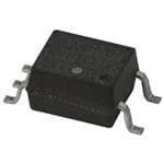
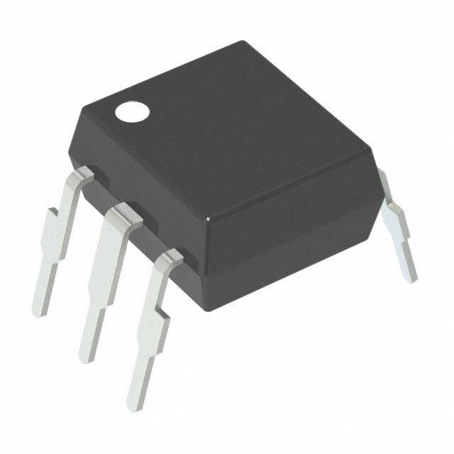
| 产品图片 |
|
| rohs | 符合RoHS无铅 / 符合限制有害物质指令(RoHS)规范要求 |
| 产品系列 | 光耦合器/光电耦合器,高速光耦合器,Fairchild Semiconductor FODM8061R2OPTOPLANAR® |
| 数据手册 | |
| 产品型号 | FODM8061R2 |
| 上升/下降时间(典型值) | 20ns, 10ns |
| 上升时间 | 20 ns |
| 产品种类 | 高速光耦合器 |
| 传播延迟tpLH/tpHL(最大值) | 80ns, 80ns |
| 供应商器件封装 | 5-MFP |
| 共模瞬态抗扰度(最小值) | 20kV/µs |
| 其它名称 | FODM8061R2DKR |
| 包装 | Digi-Reel® |
| 单位重量 | 120 mg |
| 商标 | Fairchild Semiconductor |
| 安装类型 | 表面贴装 |
| 封装 | Reel |
| 封装/外壳 | 6-SMD 模块 |
| 封装/箱体 | SO-5 |
| 工作温度 | -40°C ~ 110°C |
| 工厂包装数量 | 2500 |
| 数据速率 | 10 MBd |
| 最大功率耗散 | 100 mW |
| 最大反向二极管电压 | 5 V |
| 最大工作温度 | + 110 C |
| 最小工作温度 | - 40 C |
| 标准包装 | 1 |
| 电压-正向(Vf)(典型值) | 1.45V |
| 电压-电源 | 3 V ~ 5.5 V |
| 电压-隔离 | 3750Vrms |
| 电流-DC正向(If) | 50mA |
| 电流-输出/通道 | 50mA |
| 系列 | FODM8061 |
| 绝缘电压 | 3750 Vrms |
| 输入-输入侧1/输入侧2 | 1/0 |
| 输入类型 | DC |
| 输出类型 | 开集,肖特基箝位 |
| 输出设备 | Photo IC |
| 通道数 | 1 |


- 商务部:美国ITC正式对集成电路等产品启动337调查
- 曝三星4nm工艺存在良率问题 高通将骁龙8 Gen1或转产台积电
- 太阳诱电将投资9.5亿元在常州建新厂生产MLCC 预计2023年完工
- 英特尔发布欧洲新工厂建设计划 深化IDM 2.0 战略
- 台积电先进制程称霸业界 有大客户加持明年业绩稳了
- 达到5530亿美元!SIA预计今年全球半导体销售额将创下新高
- 英特尔拟将自动驾驶子公司Mobileye上市 估值或超500亿美元
- 三星加码芯片和SET,合并消费电子和移动部门,撤换高东真等 CEO
- 三星电子宣布重大人事变动 还合并消费电子和移动部门
- 海关总署:前11个月进口集成电路产品价值2.52万亿元 增长14.8%


PDF Datasheet 数据手册内容提取
Is Now Part of To learn more about ON Semiconductor, please visit our website at www.onsemi.com Please note: As part of the Fairchild Semiconductor integration, some of the Fairchild orderable part numbers will need to change in order to meet ON Semiconductor’s system requirements. Since the ON Semiconductor product management systems do not have the ability to manage part nomenclature that utilizes an underscore (_), the underscore (_) in the Fairchild part numbers will be changed to a dash (-). This document may contain device numbers with an underscore (_). Please check the ON Semiconductor website to verify the updated device numbers. The most current and up-to-date ordering information can be found at www.onsemi.com. Please email any questions regarding the system integration to Fairchild_questions@onsemi.com. ON Semiconductor and the ON Semiconductor logo are trademarks of Semiconductor Components Industries, LLC dba ON Semiconductor or its subsidiaries in the United States and/or other countries. ON Semiconductor owns the rights to a number of patents, trademarks, copyrights, trade secrets, and other intellectual property. A listing of ON Semiconductor’s product/patent coverage may be accessed at www.onsemi.com/site/pdf/Patent-Marking.pdf. ON Semiconductor reserves the right to make changes without further notice to any products herein. ON Semiconductor makes no warranty, representation or guarantee regarding the suitability of its products for any particular purpose, nor does ON Semiconductor assume any liability arising out of the application or use of any product or circuit, and specifically disclaims any and all liability, including without limitation special, consequential or incidental damages. Buyer is responsible for its products and applications using ON Semiconductor products, including compliance with all laws, regulations and safety requirements or standards, regardless of any support or applications information provided by ON Semiconductor. “Typical” parameters which may be provided in ON Semiconductor data sheets and/or specifications can and do vary in different applications and actual performance may vary over time. All operating parameters, including “Typicals” must be validated for each customer application by customer’s technical experts. ON Semiconductor does not convey any license under its patent rights nor the rights of others. ON Semiconductor products are not designed, intended, or authorized for use as a critical component in life support systems or any FDA Class 3 medical devices or medical devices with a same or similar classification in a foreign jurisdiction or any devices intended for implantation in the human body. Should Buyer purchase or use ON Semiconductor products for any such unintended or unauthorized application, Buyer shall indemnify and hold ON Semiconductor and its officers, employees, subsidiaries, affiliates, and distributors harmless against all claims, costs, damages, and expenses, and reasonable attorney fees arising out of, directly or indirectly, any claim of personal injury or death associated with such unintended or unauthorized use, even if such claim alleges that ON Semiconductor was negligent regarding the design or manufacture of the part. ON Semiconductor is an Equal Opportunity/Affirmative Action Employer. This literature is subject to all applicable copyright laws and is not for resale in any manner.
F O D M May 2017 8 0 6 1 — FODM8061 H High Noise Immunity, 3.3V/5V, 10Mbit/sec i g h Logic Gate Output (Open Collector) Optocoupler N o i s e Features Description I m • High Noise Immunity characterized by common mode The FODM8061 is a 3.3V/5V high-speed logic gate m transient immunity (CMTi) output (open collector) optocoupler, which supports u n isolated communications allowing digital signals to – 20kV/µs Minimum CMTi it communicate between systems without conducting y • High Speed ground loops or hazardous voltages. It utilizes Fairchild’s , 3 – 10Mbit/sec Date Rate (NRZ) patented coplanar packaging technology, Optoplanar®, .3 V – 80ns max. Propagation Delay and optimized IC design to achieve high noise immunity, / 5 – 25ns max. Pulse Width Distortion characterized by high common mode transient immunity V specifications. , – 40ns max. Propagation Delay Skew 1 0 • 3.3V LVTTL/LVCMOS Compatibility This optocoupler consists of an AlGaAS LED at the M input, optically coupled to a high speed integrated photo- b • Specifications guaranteed over 3V to 5.5V supply detector logic gate. The output of the detector IC is an it / voltage and -40°C to +110°C temperature range open collector schottky-clamped transistor. The coupled s e • Safety and regulatory approvals parameters are guaranteed over the wide temperature c range of -40°C to +110°C. A maximum input signal of L – UL1577, 3750 VACRMS for 1 min. 5mA will provide a minimum output sink current of 13mA og – IEC60747-5-2 (fan out of 8). ic G Applications Related Resources a • Microprocessor system interface t e • www.fairchildsemi.com/products/opto/ – SPI, I2C O • www.fairchildsemi.com/pf/FO/FODM611.html u • Industrial fieldbus communications t p • www.fairchildsemi.com/pf/FO/FODM8071.html u – DeviceNet, CAN, RS485 t • Programmable logic control (O p • Isolated data acquisition system e n • Voltage level translator C o • Isolating MOSFET/IGBT gate drivers l l e c t o r ) O p t o c o u p l e r ©2009 Fairchild Semiconductor Corporation www.fairchildsemi.com FODM8061 Rev. 1.1
F O D Functional Schematic M 8 0 6 Truth Table 1 ANODE 1 6 VCC — LED Output H Off High i 5 VO On Low gh N o i CATHODE 3 4 GND s e I m m u n Pin Definitions i t y , Number Name Function Description 3 . 3 1 ANODE Anode V / 3 CATHODE Cathode 5 V 4 GND Output Ground , 1 0 5 V Output Voltage O M 6 V Output Supply Voltage b CC i t / s e Safety and Insulation Ratings for Mini-Flat Package (SO5 Pin) c L As per IEC60747-5-2. This optocoupler is suitable for “safe electrical insulation” only within the safety limit data. o Compliance with the safety ratings shall be ensured by means of protective circuits. g i c Symbol Parameter Min. Typ. Max. Unit G a Installation Classifications per DIN VDE 0110/1.89 Table 1 t e For rated main voltage < 150Vrms I-IV O u For rated main voltage < 300Vrms I-III t p Climatic Classification 40/110/21 u t Pollution Degree (DIN VDE 0110/1.89) 2 ( O CTI Comparative Tracking Index 175 p e VPR Input to Output Test Voltage, Method b, 1060 n VIORM x 1.875 = VPR, 100% Production Test with C t = 1 sec, Partial Discharge < 5 pC o m l l V Input to Output Test Voltage, Method a, 848 e PR c VIORM x 1.5 = V , Type and Sample Test with t PR o t = 60 sec, Partial Discharge < 5 pC r m ) V Max Working Insulation Voltage 565 V O IORM peak p V Highest Allowable Over Voltage 4000 V t IOTM peak o External Creepage 5.0 mm c o External Clearance 5.0 mm u p Insulation thickness 0.5 mm le r T Safety Limit Values, Maximum Values allowed in the event 150 C Case of a failure, Case Temperature R Insulation Resistance at T , V = 500V 109 Ω IO S IO ©2009 Fairchild Semiconductor Corporation www.fairchildsemi.com FODM8061 Rev. 1.1 2
F O Absolute Maximum Ratings (T =25ºC unless otherwise specified) D A M Stresses exceeding the absolute maximum ratings may damage the device. The device may not function or be 8 operable above the recommended operating conditions and stressing the parts to these levels is not recommended. In 0 6 addition, extended exposure to stresses above the recommended operating conditions may affect device reliability. 1 The absolute maximum ratings are stress ratings only. — Symbol Parameter Value Units H i g T Storage Temperature -40 to +125 ºC STG h T Operating Temperature -40 to +110 ºC N OPR o TJ Junction Temperature -40 to +125 ºC is T Lead Solder Temperature 260 for 10sec ºC e SOL I (Refer to Reflow Temperature Profile) m m I Forward Current 50 mA F u VR Reverse Voltage 5.0 V n i VCC Supply Voltage 0 to 7.0 V ty , V Output Voltage -0.5 to V +0.5 V 3 O CC . 3 IO Average Output Current 50 mA V PD Input Power Dissipation(1)(2) 100 mW /5 I V PDO Output Power Dissipation(1)(2) 85 mW , 1 0 M Recommended Operating Conditions b The Recommended Operating Conditions table defines the conditions for actual device operation. Recommended it / operating conditions are specified to ensure optimal performance to the datasheet specifications. Fairchild does not s e recommend exceeding them or designing to Absolute Maximum Ratings. c L Symbol Parameter Min. Max. Unit o g TA Ambient Operating Temperature -40 +110 ºC ic V V Supply Voltages(3) 3.0 5.5 V G CC, DD a V Logic Low Input Voltage 0 0.8 V t FL e I Logic High Input Current(4) 6.3 15 mA O FH u IFL Logic Low Input Current 250 µA t p N Fan Out (at R = 1kΩ) 5 TTL Loads u L t RL Output Pull-up Resistor 330 4k Ω (O p Isolation Characteristics (TA=25ºC) en C Symbol Parameter Test Conditions Min. Typ. Max. Units o l l V Input-Output Isolation Voltage freq= 60Hz, t = 1.0min, 3750 e ISO VAC c I ≤ 10µA(5)(6) RMS t I-O o RISO Isolation Resistance VI-O = 500V(5) 1012 Ω r) C Isolation Capacitance V = 0V, freq=1.0MHz(5) 0.6 pF O ISO I-O p t o Notes: c o 1. No derate required to 110ºC. u p 2. Functional operation under these conditions is not implied. Permanent damage may occur if the device is subjected l e to conditions outside these ratings. r 3. 0.1µF bypass capacitor must be connected between pins 4 and 6. 4. Recommended I is 9.3mA for operation above T =100ºC. FH A 5. Device is considered a two terminal device: Pins 1 and 3 are shorted, and Pins 4, 5, and 6 are shorted together. 6. 3,750 VAC for 1 minute duration is equivalent to 4,500 VAC for 1 second duration. RMS RMS ©2009 Fairchild Semiconductor Corporation www.fairchildsemi.com FODM8061 Rev. 1.1 3
F O Electrical Characteristics (Apply over all recommended conditions) D M (T = -40ºC to +110ºC, 3.0V ≤ V ≤ 5.5V), unless otherwise specified. A CC 8 Typical value is measured at TA = 25ºC and VCC = 3.3V. 0 6 1 Symbol Parameter Test Conditions Min. Typ. Max. Units — INPUT CHARACTERISTICS H VF Forward Voltage IF = 10mA, Fig. 1 1.05 1.45 1.8 V ig h BV Input Reverse Breakdown Voltage I = 10µA 5.0 V R R N IFHL Threshold Input Current VO = 0.6V, IOL(sinking) = 13mA, o T < 85ºC, Fig. 2 3.4 5.0 mA is A e T = 85ºC to 110 ºC 4.2 7.5 A Im OUTPUT CHARACTERISTICS m u V Logic LOW Output Voltage I = rated I , 0.4 0.6 V OL F FHL n I (sinking) = 13mA, Fig.3 i OL t y IOH Logic HIGH Output Current IF = 250µA, VO = 3.3V, Fig. 4 8.0 50.0 µA , 3 . I = 250µA, V = 5.0V, Fig. 4 2.1 30.0 µA 3 F O V ICCL Logic LOW Output Supply Current IF = 10mA, VCC = 3.3V, Fig. 5, 7 6.0 8.5 mA /5 V , IF = 10mA, VCC = 5.0V, Fig. 5, 7 7.5 10.0 mA 1 0 I Logic HIGH Output Supply Current I = 0mA, V = 3.3V, Fig. 6, 7 4.0 7.0 mA M CCH F CC b IF = 0mA, VCC = 5.0V, Fig. 6, 7 6.0 9.0 mA it/ s e c Switching Characteristics (Apply over all recommended conditions) L (T = -40ºC to +110ºC, 3.0V ≤ V ≤ 5.5V, I = 7.5mA), unless otherwise specified. o A CC F g Typical value is measured at TA = 25ºC and VCC = 3.3V ic Symbol Parameter Test Conditions Min. Typ. Max. Units G a Date Rate RL = 350Ω 10 Mbps te t Propagation Delay Time to Logic R = 350Ω, C = 15pF, 43 80 ns O PHL L L u Low Output Fig. 8 and 11 t p tPLH Propagation Delay Time to Logic RL = 350Ω, CL = 15pF, 50 80 ns u High Output Fig. 8 and 11 t ( O PWD Pulse Width Distortion, R = 350Ω, C = 15pF, 7 25 ns L L p | tPHL - tPLH| Fig. 9 e n tPSK Propagation Delay Skew RL = 350Ω, CL = 15pF(7) 40 ns C o t Output Rise Time, (10% to 90%) R = 350Ω, C = 15pF, 20 ns ll R L L e Fig. 10 and 11 c t o t Output Fall Time, (90% to 10%) R = 350Ω, C = 15pF, 10 ns F L L r Fig. 10 and 11 ) O |CM | Common Mode Transient I = 0mA, V > 0.8 x V , 20 40 kV/µs p H F O CC Immunity at Output High V = 1000V(8), Fig. 12 to CM c |CM | Common Mode Transient I = 7.5mA, V < 0.8V, 20 40 kV/µs o L F O Immunity at Output Low V = 1000V(8), Fig. 12 u CM p l e Notes r 7. t is equal to the magnitude of the worst case difference in t and/or t that will be seen between any two units PSK PHL PLH from the same manufacturing date code that are operated at same case temperature (±5°C), at same operating conditions, with equal loads (R = 350Ω and C = 15pF), and with an input rise time less than 5ns. L L 8. Common mode transient immunity at output high is the maximum tolerable positive dVcm/dt on the leading edge of the common mode impulse signal, Vcm, to assure that the output will remain high. Common mode transient immunity at output low is the maximum tolerable negative dVcm/dt on the trailing edge of the common pulse signal, Vcm, to assure that the output will remain low. ©2009 Fairchild Semiconductor Corporation www.fairchildsemi.com FODM8061 Rev. 1.1 4
F O Typical Performance Curves D M 8 Fig. 1 Input LED Current vs Forward Voltage Fig. 2 Threshold Input Current vs Ambient Temperature 0 100 A) 6 IOL = 13mA 61 T (m — mA) 10 REN 5 H T ( UR i URREN 1 TA = 110°C TA = -40°C NPUT C 4 VCC = 5.0V gh N I – INPUT LED CF 00.0.11 TA = 25°C – THRESHOLD IHT 23 VCC = 3.3V oise Imm IF u n 0.001 1 it 0.6 0.8 1.0 1.2 1.4 1.6 1.8 2.0 -40 -20 0 20 40 60 80 100 120 y VF – FORWARD VOLTAGE (V) TA – AMBIENT TEMPERATURE (°C) , 3 . 3 V / 5 V Fig. 3 Low Level Output Voltage vs. Ambient Temperature Fig. 4 Logic High Output Current vs Ambient Temperature , 0.60 20 1 IOL = 13mA IF = 250μA 0 V) IF = 5mA μA) VO = 3.3V M GE ( 0.55 NT ( bi LTA RRE 15 t/s VO CU e UT 0.50 UT c P P L T T U V = 3.3V U 10 o L O CC H O g OW LEVE 0.45 VCC = 5.0V OGIC HIG 5 VCC = 3.3V ic Ga V – LOL 0.40 I – LOH VCC = 5.0V te O u 0.35 0 t -40 -20 0 20 40 60 80 100 120 -40 -20 0 20 40 60 80 100 120 p TA – AMBIENT TEMPERATURE (°C) TA – AMBIENT TEMPERATURE (°C) u t ( O p Fig. 5 Typical Logic Low Output Supply Current Fig. 6 Typical Logic High Output Supply Current GIC LOW OUTPUT SUPPLY CURRENT (mA) 1098765 IF = 10mA vs. Ambient TemperatuVreCVCC =C 5=. 03V.3V GIC HIGH OUTPUT SUPPLY CURRENT (mA) 10864 IF = 0mA vs. Ambient TemperatuVreCVCC =C 5=. 03V.3V en Collector) Optoco O 4 O u – TYPICAL LCCL 32-40 -20 0 20 40 60 80 100 120 – TYPICAL LCCH 20-40 -20 0 20 40 60 80 100 120 pler I TA – AMBIENT TEMPERATURE (°C) I TA – AMBIENT TEMPERATURE (°C) ©2009 Fairchild Semiconductor Corporation www.fairchildsemi.com FODM8061 Rev. 1.1 5
F O Typical Performance Curves (Continued) D M 8 0 Fig. 7 Typical Logic Output Supply Current 6 mA) 10 vs. Output Supply Voltage 1F0ig. 8 Typical Propagation Delay vs. Ambient Temperature 1 — T ( IF = 0mA (for ICCH), 10mA (for ICCL) Frequency = 5MHz EN TA = 25°C Duty Cycle = 50% H R IF = 7.5mA UR 8 s) 8 RL = 350Ω ig Y C Y (n h PPL ELA N PUT SU 6 ICCL TION D 6 tPLH @ VCC = 3.3V oise C OUT 4 ICCH PAGA 4 Im AL LOGI 2 – PROP 2 tPHL @ VCC = 3.3V tPHL @ VCC = 5.0V mun PIC t it Y y – T tPLH @ VCC = 5.0V , I CC 03.0 3.5 4.0 4.5 5.0 5.5 0-40 -20 0 20 40 60 80 100 120 3.3 VCC – OUTPUT SUPPLY VOLTAGE (V) TA – AMBIENT TEMPERATURE (°C) V / 5 V , 1 0 Fig. 9 Typical Pulse Width Distortion vs. Ambient Temperature Fig. 10 Typical Rise and Fall Time vs. Ambient Temperature M DISTORTION (ns) 108 FDIRFruL e= t=qy 7u C3.e55ynm0ccΩlAye == 55M0%Hz VCC = 3.3V ME (ns) 4300 FDIRFruL e= t=qy 7u C3.e55ynm0ccΩlAye == 55M0%Hz tR @ VCC = 5.0V bit/sec Lo WIDTH 6 FALL TI 20 tR @ VCC = 3.3V gic | ) – PULSE PLH 42 VCC = 5.0V t, t – RISE, RF 10 ttFF @@ VVCCCC == 35..03VV Gate Ou – t tp HL u ( |tP 0-40 -20 0 20 40 60 80 100 120 0-40 -20 0 20 40 60 80 100 120 t (O TA – AMBIENT TEMPERATURE (°C) TA – AMBIENT TEMPERATURE (°C) p e n C o l l e c t o r ) O p t o c o u p l e r ©2009 Fairchild Semiconductor Corporation www.fairchildsemi.com FODM8061 Rev. 1.1 6
F O Schematics D M 8 Pulse Gen. IF 0 6 5MHz 1 tf = tr = 5ns DC = 50% 0.1μF 350Ω — Bypass VO Monitoring H Input CLNode igh Monitoring N Mode o RM is e I m m (IF = 7.5mA) un Input 50% it y , 3 tf tr .3 V 90% / 5 Output 1.5V V 1V0O%L , 1 0 tPHL tPLH M b i t / Figure 11. Test Circuit for Propagation Delay Time, Rise Time and Fall Time s e c L o IF g i c VCC G 0B.y1pμaFss 350Ω a t VO Monitoring e SW CL Node O u t p u RM t ( O VCM p e n Pulse Gen C o l l e c t VCM90% 1kV o r ) O 10% 0V p t o tr tf c o u VOH p VO (IF = 0mA) l 0.8 VCC e r 0.8V VO (IF = 7.5mA) VOL Figure 12. Test Circuit for Instantaneous Common Mode Rejection Voltage ©2009 Fairchild Semiconductor Corporation www.fairchildsemi.com FODM8061 Rev. 1.1 7
F O Package Dimensions D M 8 0 6 1 — H i g h N o i s e I m m u n i t y , 3 . 3 V / 5 V , 1 0 M b i t / s e c L o g i c G a t e O u Notes: tp 1.No standard applies to this package. u t 2.All dimensions are in millimeters. ( 3.Dimensions are exclusive of burrs, mold flash, and tie bar extrusion. O 4.Drawings filesname and revision: MKT-MFP05A. p e n C Package drawings are provided as a service to customers considering Fairchild components. Drawings may change in any manner o without notice. Please note the revision and/or date on the drawing and contact a Fairchild Semiconductor representative to verify or l l obtain the most recent revision. Package specifications do not expand the terms of Fairchild’s worldwide terms and conditions, e c specifically the warranty therein, which covers Fairchild products. t o Package drawings are provided as a service to customers considering Fairchild components. Drawings may change in any manner r ) without notice. Please note the revision and/or date on the drawing and contact a Fairchild Semiconductor representative to verify or O obtain the most recent revision. Package specifications do not expand the terms of Fairchild’s worldwide terms and conditions, p specifically the warranty therein, which covers Fairchild products. to c o u Always visit Fairchild Semiconductor’s online packaging area for the most recent package drawings: p l e http://www.fairchildsemi.com/packaging/ r ©2009 Fairchild Semiconductor Corporation www.fairchildsemi.com FODM8061 Rev. 1.1 8
F O Ordering Information D M Order Entry Identifier 8 0 Option (Example) Description 6 1 No Suffix FODM8061 Mini-Flat 5-pin, shipped in tubes (100 units per tube) — R2 FODM8061R2 Mini-Flat 5-pin, tape and reel (2,500 units per reel) H i g h All packages are lead free per JEDEC: J-STD-020B standard. N o i s Marking Information e I m m u n i t y 1 , 3 . 3 V M8061 2 / 5 V , VV X YY M 6 1 0 M b i t / 3 4 5 s e c L o g Definitions ic G 1 Fairchild logo a t 2 Device number e O 3 IEC60747-5-2 (VDE marking) u t 4 One digit year code, e.g., ‘9’ p u 5 Two digit work week ranging from ‘01’ to ‘53’ t ( O 6 Assembly package code p e n C o l l e c t o r ) O p t o c o u p l e r ©2009 Fairchild Semiconductor Corporation www.fairchildsemi.com FODM8061 Rev. 1.1 9
F O Tape and Reel Dimensions D M 8 P D 0 2 0 6 P K0 t 0 E 1 — H i g A h 0 W W B N 1 0 F o i s e I m d P D 1 m u n i t 2.54 Pitch y , 3 Description Symbol Dimensions (mm) . 3 Tape Width W 12.00 +0.30/-0.10 V / 5 Tape Thickness t 0.30 ±0.05 V , Sprocket Hole Pitch P 4.00 ±0.10 1 0 0 Sprocket Hole Diameter D 1.50 +0.10/-0.0 M 0 b Sprocket Hole Location E 1.75 ±0.10 i t / Pocket Location F 5.50 ±0.10 s e P2 2.00 ±0.10 c L Pocket Pitch P 8.00 ±0.10 o g Pocket Dimension A0 4.40 ±0.10 ic B 7.30 ±0.10 G 0 a K 2.30 ±0.10 t 0 e Pocket Hole Diameter D 1.50 Min. O 1 u Cover Tape Width W1 9.20 tp Cover Tape Thickness d 0.065 ±0.010 u t Max. Component Rotation or Tilt 10° Max. (O p Devices Per Reel 2500 e n Reel Diameter 330mm (13") C o l l e c t o r ) O p t o c o u p l e r ©2009 Fairchild Semiconductor Corporation www.fairchildsemi.com FODM8061 Rev. 1.1 10
F O Reflow Profile D M 8 Max. Ramp-up Rate = 3°C/S 0 260 TP Max. Ramp-down Rate = 6°C/S 6 1 240 tP — TL 220 H 200 Tsmax i g C) 180 Preheat Area tL h ° ( 160 Tsmin No re 140 is u ts e at 120 I r m e 100 p m m 80 u e n T 60 i t 40 y , 20 3 . 3 0 V 120 240 360 /5 V Time 25°C to Peak , 1 Time (seconds) 0 M b i t / s e Profile Feature Pb-Free Assembly Profile c L Temperature Min. (Tsmin) 150°C o g Temperature Max. (Tsmax) 200°C i c Time (tS) from (Tsmin to Tsmax) 60–120 seconds G a Ramp-up Rate (t to t ) 3°C/second max. L P t e Liquidous Temperature (TL) 217°C O u Time (t ) Maintained Above (T ) 60–150 seconds L L t p Peak Body Package Temperature 260°C +0°C / –5°C u t Time (t ) within 5°C of 260°C 30 seconds ( P O Ramp-down Rate (T to T ) 6°C/second max. p P L e Time 25°C to Peak Temperature 8 minutes max. n C o l l e c t o r ) O p t o c o u p l e r ©2009 Fairchild Semiconductor Corporation www.fairchildsemi.com FODM8061 Rev. 1.1 11
ON Semiconductor and are trademarks of Semiconductor Components Industries, LLC dba ON Semiconductor or its subsidiaries in the United States and/or other countries. ON Semiconductor owns the rights to a number of patents, trademarks, copyrights, trade secrets, and other intellectual property. A listing of ON Semiconductor’s product/patent coverage may be accessed at www.onsemi.com/site/pdf/Patent−Marking.pdf. ON Semiconductor reserves the right to make changes without further notice to any products herein. ON Semiconductor makes no warranty, representation or guarantee regarding the suitability of its products for any particular purpose, nor does ON Semiconductor assume any liability arising out of the application or use of any product or circuit, and specifically disclaims any and all liability, including without limitation special, consequential or incidental damages. Buyer is responsible for its products and applications using ON Semiconductor products, including compliance with all laws, regulations and safety requirements or standards, regardless of any support or applications information provided by ON Semiconductor. “Typical” parameters which may be provided in ON Semiconductor data sheets and/or specifications can and do vary in different applications and actual performance may vary over time. All operating parameters, including “Typicals” must be validated for each customer application by customer’s technical experts. ON Semiconductor does not convey any license under its patent rights nor the rights of others. ON Semiconductor products are not designed, intended, or authorized for use as a critical component in life support systems or any FDA Class 3 medical devices or medical devices with a same or similar classification in a foreign jurisdiction or any devices intended for implantation in the human body. Should Buyer purchase or use ON Semiconductor products for any such unintended or unauthorized application, Buyer shall indemnify and hold ON Semiconductor and its officers, employees, subsidiaries, affiliates, and distributors harmless against all claims, costs, damages, and expenses, and reasonable attorney fees arising out of, directly or indirectly, any claim of personal injury or death associated with such unintended or unauthorized use, even if such claim alleges that ON Semiconductor was negligent regarding the design or manufacture of the part. ON Semiconductor is an Equal Opportunity/Affirmative Action Employer. This literature is subject to all applicable copyright laws and is not for resale in any manner. PUBLICATION ORDERING INFORMATION LITERATURE FULFILLMENT: N. American Technical Support: 800−282−9855 Toll Free ON Semiconductor Website: www.onsemi.com Literature Distribution Center for ON Semiconductor USA/Canada 19521 E. 32nd Pkwy, Aurora, Colorado 80011 USA Europe, Middle East and Africa Technical Support: Order Literature: http://www.onsemi.com/orderlit Phone: 303−675−2175 or 800−344−3860 Toll Free USA/Canada Phone: 421 33 790 2910 Fax: 303−675−2176 or 800−344−3867 Toll Free USA/Canada Japan Customer Focus Center For additional information, please contact your local Email: orderlit@onsemi.com Phone: 81−3−5817−1050 Sales Representative © Semiconductor Components Industries, LLC www.onsemi.com www.onsemi.com 1
Mouser Electronics Authorized Distributor Click to View Pricing, Inventory, Delivery & Lifecycle Information: O N Semiconductor: FODM8061V FODM8061R2V FODM8061 FODM8061R2