ICGOO在线商城 > 集成电路(IC) > 逻辑 - 缓冲器,驱动器,接收器,收发器 > 74LVC245APW,118
 Datasheet下载
- 型号: 74LVC245APW,118
- 制造商: NXP Semiconductors
- 库位|库存: xxxx|xxxx
- 要求:
| 数量阶梯 | 香港交货 | 国内含税 |
| +xxxx | $xxxx | ¥xxxx |
查看当月历史价格
查看今年历史价格
74LVC245APW,118产品简介:
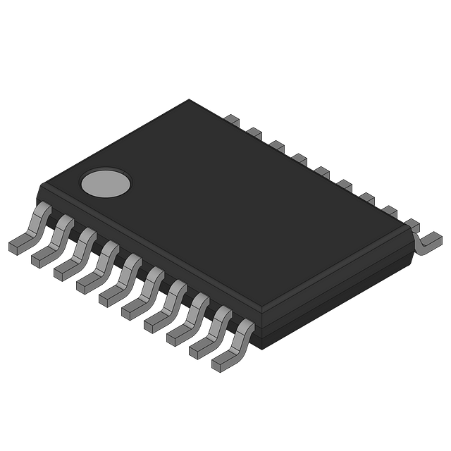
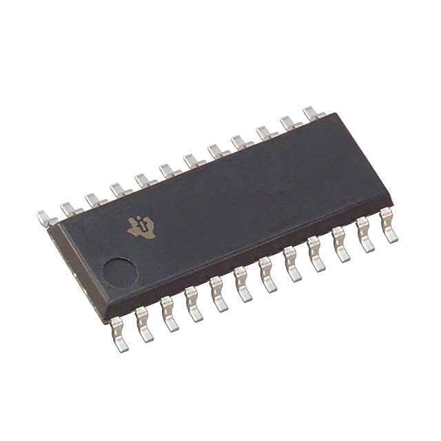
ICGOO电子元器件商城为您提供74LVC245APW,118由NXP Semiconductors设计生产,在icgoo商城现货销售,并且可以通过原厂、代理商等渠道进行代购。 74LVC245APW,118价格参考。NXP Semiconductors74LVC245APW,118封装/规格:逻辑 - 缓冲器,驱动器,接收器,收发器, Transceiver, Non-Inverting 1 Element 8 Bit per Element 3-State Output 20-TSSOP。您可以下载74LVC245APW,118参考资料、Datasheet数据手册功能说明书,资料中有74LVC245APW,118 详细功能的应用电路图电压和使用方法及教程。
Nexperia USA Inc. 的 74LVC245APW,118 是一款八路总线收发器,属于逻辑缓冲器/驱动器/接收器/收发器类别。该器件采用TSSOP20封装,工作电压范围为1.65V至5.5V,兼容低电压CMOS和TTL电平,适用于多种数字系统间的电平转换与信号隔离。

其主要应用场景包括:工业控制系统的数字信号传输、通信设备中的数据总线驱动、消费类电子产品(如智能家居设备、平板电脑)中的板级信号缓冲与隔离。由于具备双向数据传输能力并支持三态输出,该芯片常用于微处理器与外设之间的数据总线管理,有效提升信号完整性和抗干扰能力。

此外,74LVC245APW,118 也广泛应用于嵌入式系统、测试仪器及汽车电子模块中,作为地址/数据总线的驱动与隔离器件。其高噪声抑制特性和低功耗设计使其在电磁环境复杂的场景下仍能稳定运行。总体而言,该芯片适用于需要高效、可靠数字信号传输的中低速逻辑接口应用。
| 参数 | 数值 |
| 产品目录 | 集成电路 (IC)半导体 |
| 描述 | IC TRANSCVR TRI-ST 8BIT 20TSSOP总线收发器 3.3V OCTAL TRNSCEIVER 3-S |
| 产品分类 | |
| 品牌 | NXP Semiconductors |
| 产品手册 | |
| 产品图片 |
|
| rohs | 符合RoHS无铅 / 符合限制有害物质指令(RoHS)规范要求 |
| 产品系列 | 逻辑集成电路,总线收发器,NXP Semiconductors 74LVC245APW,11874LVC |
| 数据手册 | |
| 产品型号 | 74LVC245APW,118 |
| PCN封装 | |
| 产品培训模块 | http://www.digikey.cn/PTM/IndividualPTM.page?site=cn&lang=zhs&ptm=24983 |
| 产品目录页面 | |
| 产品种类 | 总线收发器 |
| 传播延迟时间 | 17 ns |
| 低电平输出电流 | 24 mA |
| 供应商器件封装 | 20-TSSOP |
| 元件数 | 1 |
| 其它名称 | 568-2301-1 |
| 功能 | Bus Transceiver |
| 包装 | 剪切带 (CT) |
| 商标 | NXP Semiconductors |
| 安装类型 | 表面贴装 |
| 安装风格 | SMD/SMT |
| 封装 | Reel |
| 封装/外壳 | 20-TSSOP(0.173",4.40mm 宽) |
| 封装/箱体 | TSSOP-20 |
| 工作温度 | -40°C ~ 125°C |
| 工厂包装数量 | 2500 |
| 最大工作温度 | + 125 C |
| 最小工作温度 | - 40 C |
| 极性 | Non-Inverting |
| 标准包装 | 1 |
| 每元件位数 | 8 |
| 每芯片的通道数量 | 8 |
| 电压-电源 | 1.65 V ~ 3.6 V |
| 电流-输出高,低 | 24mA,24mA |
| 电源电压-最大 | 3.6 V |
| 电源电压-最小 | 1.2 V |
| 电路数量 | 1 |
| 输入电平 | LVTTL |
| 输出电平 | LVTTL |
| 输出类型 | 3-State |
| 逻辑类型 | 收发器,非反相 |
| 逻辑系列 | LVC |
| 零件号别名 | 74LVC245APW-T |
| 高电平输出电流 | - 24 mA |

.jpg)


- 商务部:美国ITC正式对集成电路等产品启动337调查
- 曝三星4nm工艺存在良率问题 高通将骁龙8 Gen1或转产台积电
- 太阳诱电将投资9.5亿元在常州建新厂生产MLCC 预计2023年完工
- 英特尔发布欧洲新工厂建设计划 深化IDM 2.0 战略
- 台积电先进制程称霸业界 有大客户加持明年业绩稳了
- 达到5530亿美元!SIA预计今年全球半导体销售额将创下新高
- 英特尔拟将自动驾驶子公司Mobileye上市 估值或超500亿美元
- 三星加码芯片和SET,合并消费电子和移动部门,撤换高东真等 CEO
- 三星电子宣布重大人事变动 还合并消费电子和移动部门
- 海关总署:前11个月进口集成电路产品价值2.52万亿元 增长14.8%


PDF Datasheet 数据手册内容提取
74LVC245A; 74LVCH245A Octal bus transceiver; 3-state Rev. 9 — 11 September 2018 Product data sheet 1. General description The 74LVC245A; 74LVCH245A are 8-bit transceivers featuring non-inverting 3-state bus compatible outputs in both send and receive directions. The device features an output enable (OE) input for easy cascading and a send/receive (DIR) input for direction control. OE controls the outputs so that the buses are effectively isolated. Inputs can be driven from either 3.3 V or 5 V devices. When disabled, up to 5.5 V can be applied to the outputs. These features allow the use of these devices in mixed 3.3 V and 5 V applications. The 74LVCH245A bus hold on data inputs eliminates the need for external pull-up resistors to hold unused inputs. 2. Features and benefits • 5 V tolerant inputs/outputs for interfacing with 5 V logic • Wide supply voltage range from 1.2 V to 3.6 V • CMOS low-power consumption • Direct interface with TTL levels • Inputs accept voltages up to 5.5 V • High-impedance when V = 0 V CC • Bus hold on all data inputs (74LVCH245A only) • Complies with JEDEC standard: • JESD8-7A (1.65 V to 1.95 V) • JESD8-5A (2.3 V to 2.7 V) • JESD8-C/JESD36 (2.7 V to 3.6 V) • ESD protection: • HBM JESD22-A114F exceeds 2000 V • MM JESD22-A115B exceeds 200 V • CDM JESD22-C101E exceeds 1000 V • Specified from -40 °C to +85 °C and -40 °C to +125 °C
Nexperia 74LVC245A; 74LVCH245A Octal bus transceiver; 3-state 3. Ordering information Table 1. Ordering information Type number Package Temperature range Name Description Version 74LVC245AD -40 °C to +125 °C SO20 plastic small outline package; 20 leads; SOT163-1 body width 7.5 mm 74LVCH245AD 74LVC245ADB -40 °C to +125 °C SSOP20 plastic shrink small outline package; 20 leads; SOT339-1 body width 5.3 mm 74LVCH245ADB 74LVC245APW -40 °C to +125 °C TSSOP20 plastic thin shrink small outline package; SOT360-1 20 leads; body width 4.4 mm 74LVCH245APW 74LVC245ABQ -40 °C to +125 °C DHVQFN20 plastic dual in-line compatible SOT764-1 thermal enhanced very thin quad 74LVCH245ABQ flat package; no leads; 20 terminals; body 2.5 × 4.5 × 0.85 mm 4. Functional diagram DIR 1 OE 19 A0 2 B0 18 A1 3 B1 17 A2 4 19 G3 B2 1 16 3EN1 A3 3EN2 5 B3 15 1 A4 2 18 6 2 B4 14 3 17 A5 7 4 16 B5 13 5 15 A6 8 6 14 B6 12 7 13 A7 9 8 12 B7 11 9 11 mna174 mna175 Fig. 1. Logic diagram Fig. 2. IEC logic symbol 74LVC_LVCH245A All information provided in this document is subject to legal disclaimers. © Nexperia B.V. 2018. All rights reserved Product data sheet Rev. 9 — 11 September 2018 2 / 16
Nexperia 74LVC245A; 74LVCH245A Octal bus transceiver; 3-state 5. Pinning information 5.1. Pinning 74LVC245A 74LVCH245A itnedrmexin aarle 1a DIR VCC 1 20 A0 2 19 OE A1 3 18 B0 A2 4 17 B1 A3 5 16 B2 74LVC245A 74LVCH245A A4 6 15 B3 A5 7 14 B4 DIR 1 20 VCC A0 2 19 OE A6 8 GND(1) 13 B5 A1 3 18 B0 A7 9 12 B6 0 1 A2 4 17 B1 1 1 D 7 A3 5 16 B2 N B 001aak293 G A4 6 15 B3 Transparent top view A5 7 14 B4 (1) This is not a supply pin. The substrate is A6 8 13 B5 attached to this pad using conductive die attach A7 9 12 B6 material. There is no electrical or mechanical GND 10 11 B7 requirement to solder this pad. However, if it is 001aak292 soldered, the solder land should remain floating or be connected to GND. Fig. 3. Pin configuration SOT163-1 (SO20), SOT339-1 (SSOP20) and SOT360-1 (TSSOP20) Fig. 4. Pin configuration SOT764-1 (DHVQFN20) 5.2. Pin description Table 2. Pin description Symbol Pin Description DIR 1 direction control A0, A1, A2, A3, A4, A5, A6, A7 2, 3, 4, 5, 6, 7, 8, 9 data input/output GND 10 ground (0 V) B0, B1, B2, B3, B4, B5, B6, B7 18, 17, 16, 15, 14, 13, 12, 11 data input/output OE 19 output enable input (active LOW) V 20 supply voltage CC 6. Functional description Table 3. Function selection H = HIGH voltage level; L = LOW voltage level; X = don’t care; Z = high impedance OFF-state. Inputs Inputs/outputs OE DIR An Bn L L An = Bn inputs L H inputs Bn = An H X Z Z 74LVC_LVCH245A All information provided in this document is subject to legal disclaimers. © Nexperia B.V. 2018. All rights reserved Product data sheet Rev. 9 — 11 September 2018 3 / 16
Nexperia 74LVC245A; 74LVCH245A Octal bus transceiver; 3-state 7. Limiting values Table 4. Limiting values In accordance with the Absolute Maximum Rating System (IEC 60134). Voltages are referenced to GND (ground = 0 V). Symbol Parameter Conditions Min Max Unit V supply voltage -0.5 +6.5 V CC I input clamping current V < 0 V -50 - mA IK I V input voltage [1] -0.5 +6.5 V I I output clamping current V > V or V < 0 V - ±50 mA OK O CC O V output voltage output HIGH or LOW [2] -0.5 V + 0.5 V O CC output 3-state [2] -0.5 +6.5 V I output current V = 0 V to V - ±50 mA O O CC I supply current - 100 mA CC I ground current -100 - mA GND T storage temperature -65 +150 °C stg P total power dissipation T = -40 °C to +125 °C [3] - 500 mW tot amb [1] The minimum input voltage ratings may be exceeded if the input current ratings are observed. [2] The output voltage ratings may be exceeded if the output current ratings are observed. [3] For SO20 packages: above 70 °C derate linearly with 8 mW/K. For (T)SSOP20 packages: above 60 °C derate linearly with 5.5 mW/K. For DHVQFN20 packages: above 60 °C derate linearly with 4.5 mW/K. 8. Recommended operating conditions Table 5. Recommended operating conditions Symbol Parameter Conditions Min Typ Max Unit V supply voltage 1.65 - 3.6 V CC functional 1.2 - 3.6 V V input voltage 0 - 5.5 V I V output voltage output HIGH or LOW 0 - V V O CC output 3-state 0 - 5.5 V T ambient temperature in free air -40 - +125 °C amb Δt/ΔV input transition rise and fall rate V = 1.2 V to 2.7 V 0 - 20 ns/V CC V = 2.7 V to 3.6 V 0 - 10 ns/V CC 74LVC_LVCH245A All information provided in this document is subject to legal disclaimers. © Nexperia B.V. 2018. All rights reserved Product data sheet Rev. 9 — 11 September 2018 4 / 16
Nexperia 74LVC245A; 74LVCH245A Octal bus transceiver; 3-state 9. Static characteristics Table 6. Static characteristics At recommended operating conditions. Voltages are referenced to GND (ground = 0 V). Symbol Parameter Conditions T = -40 °C to +85 °C T = Unit amb amb -40 °C to +125 °C Min Typ [1] Max Min Max V HIGH-level input V = 1.2 V 1.08 - - 1.08 - V IH CC voltage V = 1.65 V to 1.95 V 0.65V - - 0.65V - V CC CC CC V = 2.3 V to 2.7 V 1.7 - - 1.7 - V CC V = 2.7 V to 3.6 V 2.0 - - 2.0 - V CC V LOW-level input V = 1.2 V - - 0.12 - 0.12 V IL CC voltage V = 1.65 V to 1.95 V - - 0.35V - 0.35V V CC CC CC V = 2.3 V to 2.7 V - - 0.7 - 0.7 V CC V = 2.7 V to 3.6 V - - 0.8 - 0.8 V CC V HIGH-level V = V or V OH I IH IL output voltage I = -100 μA; V - 0.2 - - V - 0.3 - V O CC CC V = 1.65 V to 3.6 V CC I = -4 mA; V = 1.65 V 1.2 - - 1.05 - V O CC I = -8 mA; V = 2.3 V 1.8 - - 1.65 - V O CC I = -12 mA; V = 2.7 V 2.2 - - 2.05 - V O CC I = -18 mA; V = 3.0 V 2.4 - - 2.25 - V O CC I = -24 mA; V = 3.0 V 2.2 - - 2.0 - V O CC V LOW-level output V = V or V OL I IH IL voltage I = 100 μA; - - 0.2 - 0.3 V O V = 1.65 V to 3.6 V CC I = 4 mA; V = 1.65 V - - 0.45 - 0.65 V O CC I = 8 mA; V = 2.3 V - - 0.6 - 0.8 V O CC I = 12 mA; V = 2.7 V - - 0.4 - 0.6 V O CC I = 24 mA; V = 3.0 V - - 0.55 - 0.8 V O CC I input leakage V = 5.5 V or GND; [2] - ±0.1 ±5 - ±20 μA I I current V = 3.6 V CC I OFF-state output V = V or V ; [3] - ±0.1 ±5 - ±20 μA OZ I IH IL current V = 5.5 V or GND; O V = 3.6 V CC I power-off V or V = 5.5 V; V = 0.0 V - ±0.1 ±10 - ±20 μA OFF I O CC leakage current I supply current V = V or GND; I = 0 A; - 0.1 10 - 40 μA CC I CC O V = 3.6 V CC ΔI additional supply per input pin; V = V - 0.6 V; - 5 500 - 5000 μA CC I CC current I = 0 A; V = 2.7 V to 3.6 V O CC C input capacitance V = 0 V to 3.6 V; - 4.0 - - - pF I CC V = GND to V I CC C input/output V = 0 V to 3.6 V; - 10 - - - pF I/O CC capacitance V = GND to V I CC 74LVC_LVCH245A All information provided in this document is subject to legal disclaimers. © Nexperia B.V. 2018. All rights reserved Product data sheet Rev. 9 — 11 September 2018 5 / 16
Nexperia 74LVC245A; 74LVCH245A Octal bus transceiver; 3-state Symbol Parameter Conditions T = -40 °C to +85 °C T = Unit amb amb -40 °C to +125 °C Min Typ [1] Max Min Max I bus hold LOW V = 1.65; V = 0.58 V [4][5] 10 - - 10 - μA BHL CC I current V = 2.3; V = 0.7 V 30 - - 25 - μA CC I V = 3.0; V = 0.8 V 75 - - 60 - μA CC I I bus hold V = 1.65; V = 1.07 V [4][5] -10 - - -10 - μA BHH CC I HIGH current V = 2.3; V = 1.7 V -30 - - -25 - μA CC I V = 3.0; V = 2.0 V -75 - - -60 - μA CC I I bus hold LOW V = 1.95 V [4][6] 200 - - 200 - μA BHLO CC overdrive current V = 2.7 V 300 - - 300 - μA CC V = 3.6 V 500 - - 500 - μA CC I bus hold HIGH V = 1.95 V [4][6] -200 - - -200 - μA BHHO CC overdrive current V = 2.7 V -300 - - -300 - μA CC V = 3.6 V -500 - - -500 - μA CC [1] All typical values are measured at VCC = 3.3 V (unless stated otherwise) and Tamb = 25 °C. [2] The bus hold circuit is switched off when VI ˃ VCC allowing 5.5 V on the input terminal. [3] For I/O ports the parameter IOZ includes the input leakage current. [4] Valid for data inputs of bus hold parts only (74LVCH245A). Note that control inputs do not have a bus hold circuit. [5] The specified sustaining current at the data input holds the input below the specified VI level. [6] The specified overdrive current at the data input forces the data input to the opposite input state. 74LVC_LVCH245A All information provided in this document is subject to legal disclaimers. © Nexperia B.V. 2018. All rights reserved Product data sheet Rev. 9 — 11 September 2018 6 / 16
Nexperia 74LVC245A; 74LVCH245A Octal bus transceiver; 3-state 10. Dynamic characteristics Table 7. Dynamic characteristics Voltages are referenced to GND (ground = 0 V). For test circuit see Fig. 7. Symbol Parameter Conditions T = -40 °C to +85 °C T = Unit amb amb -40 °C to +125 °C Min Typ [1] Max Min Max t propagation nAn to nBn; nBn to nAn; see Fig. 5 [2] pd delay V = 1.2 V - 17.0 - - - ns CC V = 1.65 V to 1.95 V 1.5 6.5 14.6 1.5 16.9 ns CC V = 2.3 V to 2.7 V 1.0 3.4 7.6 1.0 8.7 ns CC V = 2.7 V 1.5 3.4 7.3 1.5 9.5 ns CC V = 3.0 V to 3.6 V 1.5 2.9 6.3 1.5 8.0 ns CC t enable time nOE to nAn, nBn; see Fig. 6 [2] en V = 1.2 V - 22.0 - - - ns CC V = 1.65 V to 1.95 V 1.9 8.3 19.5 1.9 22.5 ns CC V = 2.3 V to 2.7 V 1.5 4.6 10.7 1.5 12.4 ns CC V = 2.7 V 1.5 4.8 9.5 1.5 12.0 ns CC V = 3.0 V to 3.6 V 1.5 3.7 8.5 1.5 11.0 ns CC t disable time nOE to nAn, nBn; see Fig. 6 [2] dis V = 1.2 V - 12.0 - - - ns CC V = 1.65 V to 1.95 V 2.9 5.5 12.3 2.9 14.2 ns CC V = 2.3 V to 2.7 V 1.0 3.1 7.1 1.0 8.2 ns CC V = 2.7 V 1.5 3.9 8.0 1.5 10.0 ns CC V = 3.0 V to 3.6 V 1.7 3.6 7.0 1.7 9.0 ns CC t output skew [3] - - 1.0 - 1.5 ns sk(o) time C power per input; V = GND to V [4] PD I CC dissipation V = 1.65 V to 1.95 V - 7.7 - - - pF CC capacitance V = 2.3 V to 2.7 V - 11.3 - - - pF CC V = 3.0 V to 3.6 V - 14.4 - - - pF CC [1] Typical values are measured at Tamb = 25 °C and VCC = 1.2 V, 1.8 V, 2.5 V, 2.7 V and 3.3 V respectively. [2] tpd is the same as tPLH and tPHL. ten is the same as tPZL and tPZH. tdis is the same as tPLZ and tPHZ. [3] Skew between any two outputs of the same package switching in the same direction. This parameter is guaranteed by design. [4] CPD is used to determine the dynamic power dissipation (PD in μW). PD = CPD × VCC2 × fi × N + Σ(CL × VCC2 × fo) where: fi = input frequency in MHz; fo = output frequency in MHz CL = output load capacitance in pF VCC = supply voltage in Volts N = number of inputs switching Σ(CL × VCC2 × fo) = sum of the outputs. 74LVC_LVCH245A All information provided in this document is subject to legal disclaimers. © Nexperia B.V. 2018. All rights reserved Product data sheet Rev. 9 — 11 September 2018 7 / 16
Nexperia 74LVC245A; 74LVCH245A Octal bus transceiver; 3-state 10.1. Waveforms and test circuit VI An, Bn input VM VM GND tPLH tPHL VOH Bn, An output VM VM VOL mna176 See Table 8 for measurement points. V and V are typical output voltage levels that occur with the output load. OL OH Fig. 5. Input (An, Bn) to output (Bn, An) propagation delays and output transition times VI OE input VM GND tPLZ tPZL VCC output LOW-to-OFF VM OFF-to-LOW VOL VX tPHZ tPZH output VOH VY HIGH-to-OFF VM OFF-to-HIGH GND outputs outputs outputs enabled disabled enabled mna367 See Table 8 for measurement points. V and V are typical output voltage levels that occur with the output load. OL OH Fig. 6. Enable and disable times Table 8. Measurement points Supply voltage V Input M V V V V CC I X Y 1.2 V 0.5 × V V V + 0.15 V V - 0.15 V CC CC OL OH 1.65 V to 1.95 V 0.5 × V V V + 0.15 V V - 0.15 V CC CC OL OH 2.3 V to 2.7 V 0.5 × V V V + 0.15 V V - 0.15 V CC CC OL OH 2.7 V 1.5 V 2.7 V V + 0.3 V V - 0.3 V OL OH 3.0 V to 3.6 V 1.5 V 2.7 V V + 0.3 V V - 0.3 V OL OH 74LVC_LVCH245A All information provided in this document is subject to legal disclaimers. © Nexperia B.V. 2018. All rights reserved Product data sheet Rev. 9 — 11 September 2018 8 / 16
Nexperia 74LVC245A; 74LVCH245A Octal bus transceiver; 3-state tW VI 90 % negative pulse VM VM 10 % 0 V tf tr tr tf VI 90 % positive pulse VM VM 10 % 0 V tW VEXT VCC RL VI VO G DUT RT CL RL 001aae331 Test data is given in Table 9. Definitions for test circuit: R = Load resistance. L C = Load capacitance including jig and probe capacitance. L R = Termination resistance should be equal to output impedance Z of the pulse generator. T o V = External voltage for measuring switching times. EXT Fig. 7. Test circuit for measuring switching times Table 9. Test data Supply voltage Input Load V EXT V t, t C R t , t t , t t , t I r f L L PLH PHL PLZ PZL PHZ PZH 1.2 V V ≤ 2 ns 30 pF 1 kΩ open 2 × V GND CC CC 1.65 V to 1.95 V V ≤ 2 ns 30 pF 1 kΩ open 2 × V GND CC CC 2.3 V to 2.7 V V ≤ 2 ns 30 pF 500 Ω open 2 × V GND CC CC 2.7 V 2.7 V ≤ 2.5 ns 50 pF 500 Ω open 2 × V GND CC 3.0 V to 3.6 V 2.7 V ≤ 2.5 ns 50 pF 500 Ω open 2 × V GND CC 74LVC_LVCH245A All information provided in this document is subject to legal disclaimers. © Nexperia B.V. 2018. All rights reserved Product data sheet Rev. 9 — 11 September 2018 9 / 16
Nexperia 74LVC245A; 74LVCH245A Octal bus transceiver; 3-state 11. Package outline SO20: plastic small outline package; 20 leads; body width 7.5 mm SOT163-1 D E A X c y H E v M A Z 20 11 Q A 2 A A 1 (A 3 ) pin 1 index θ L p L 1 10 detail X e w M b p 0 5 10 mm scale DIMENSIONS (inch dimensions are derived from the original mm dimensions) UNIT mAax . A 1 A 2 A 3 b p c D (1) E (1) e H E L L p Q v w y Z (1) θ 0.3 2.45 0.49 0.32 13.0 7.6 10.65 1.1 1.1 0.9 mm 2.65 0.25 1.27 1.4 0.25 0.25 0.1 0.1 2.25 0.36 0.23 12.6 7.4 10.00 0.4 1.0 0.4 8 o 0.012 0.096 0.019 0.013 0.51 0.30 0.419 0.043 0.043 0.035 0 o inches 0.1 0.01 0.05 0.055 0.01 0.01 0.004 0.004 0.089 0.014 0.009 0.49 0.29 0.394 0.016 0.039 0.016 Note 1. Plastic or metal protrusions of 0.15 mm (0.006 inch) maximum per side are not included. OUTLINE REFERENCES EUROPEAN ISSUE DATE VERSION IEC JEDEC JEITA PROJECTION 99-12-27 SOT163-1 075E04 MS-013 03-02-19 Fig. 8. Package outline SOT163-1 (SO20) 74LVC_LVCH245A All information provided in this document is subject to legal disclaimers. © Nexperia B.V. 2018. All rights reserved Product data sheet Rev. 9 — 11 September 2018 10 / 16
Nexperia 74LVC245A; 74LVCH245A Octal bus transceiver; 3-state SSOP20: plastic shrink small outline package; 20 leads; body width 5.3 mm SOT339-1 D E A X c y H E v M A Z 20 11 Q A 2 A A 1 (A 3 ) pin 1 index θ L p L 1 10 detail X w M e b p 0 2.5 5 mm scale DIMENSIONS (mm are the original dimensions) UNIT mAax . A 1 A 2 A 3 b p c D (1) E (1) e H E L L p Q v w y Z (1) θ 0.21 1.80 0.38 0.20 7.4 5.4 7.9 1.03 0.9 0.9 8 o mm 2 0.05 1.65 0.25 0.25 0.09 7.0 5.2 0.65 7.6 1.25 0.63 0.7 0.2 0.13 0.1 0.5 0 o Note 1. Plastic or metal protrusions of 0.2 mm maximum per side are not included. OUTLINE REFERENCES EUROPEAN ISSUE DATE VERSION IEC JEDEC JEITA PROJECTION 99-12-27 SOT339-1 MO-150 03-02-19 Fig. 9. Package outline SOT339-1 (SSOP20) 74LVC_LVCH245A All information provided in this document is subject to legal disclaimers. © Nexperia B.V. 2018. All rights reserved Product data sheet Rev. 9 — 11 September 2018 11 / 16
Nexperia 74LVC245A; 74LVCH245A Octal bus transceiver; 3-state TSSOP20: plastic thin shrink small outline package; 20 leads; body width 4.4 mm SOT360-1 D E A X c y H E v M A Z 20 11 Q A 2 (A 3 ) A pin 1 index A 1 θ L p L 1 10 detail X w M e b p 0 2.5 5 mm scale DIMENSIONS (mm are the original dimensions) UNIT mAax . A 1 A 2 A 3 b p c D (1) E (2) e H E L L p Q v w y Z (1) θ 0.15 0.95 0.30 0.2 6.6 4.5 6.6 0.75 0.4 0.5 8 o mm 1.1 0.05 0.80 0.25 0.19 0.1 6.4 4.3 0.65 6.2 1 0.50 0.3 0.2 0.13 0.1 0.2 0 o Notes 1. Plastic or metal protrusions of 0.15 mm maximum per side are not included. 2. Plastic interlead protrusions of 0.25 mm maximum per side are not included. OUTLINE REFERENCES EUROPEAN ISSUE DATE VERSION IEC JEDEC JEITA PROJECTION 99-12-27 SOT360-1 MO-153 03-02-19 Fig. 10. Package outline SOT360-1 (TSSOP20) 74LVC_LVCH245A All information provided in this document is subject to legal disclaimers. © Nexperia B.V. 2018. All rights reserved Product data sheet Rev. 9 — 11 September 2018 12 / 16
Nexperia 74LVC245A; 74LVCH245A Octal bus transceiver; 3-state DHVQFN20: plastic dual in-line compatible thermal enhanced very thin quad flat package; no leads; 20 terminals; body 2.5 x 4.5 x 0.85 mm SOT764-1 D B A A A1 E c terminal 1 detail X index area terminal 1 index area e1 C v C A B e b y1C y w C 2 9 L 1 10 Eh e 20 11 19 12 Dh X 0 2.5 5 mm scale Dimensions (mm are the original dimensions) Unit A(1) A1 b c D(1) Dh E(1) Eh e e1 L v w y y1 max 1.00 0.05 0.30 4.6 3.15 2.6 1.15 0.5 mm nom 0.90 0.02 0.25 0.2 4.5 3.00 2.5 1.00 0.5 3.5 0.4 0.1 0.05 0.05 0.1 min 0.80 0.00 0.18 4.4 2.85 2.4 0.85 0.3 Note 1. Plastic or metal protrusions of 0.075 mm maximum per side are not included. sot764-1_po Outline References European Issue date version IEC JEDEC JEITA projection 03-01-27 SOT764-1 - - - MO-241 - - - 14-12-12 Fig. 11. Package outline SOT764-1 (DHVQFN20) 74LVC_LVCH245A All information provided in this document is subject to legal disclaimers. © Nexperia B.V. 2018. All rights reserved Product data sheet Rev. 9 — 11 September 2018 13 / 16
Nexperia 74LVC245A; 74LVCH245A Octal bus transceiver; 3-state 12. Abbreviations Table 10. Abbreviations Acronym Description CDM Charged Device Model CMOS Complementary Metal-Oxide Semiconductor DUT Device Under Test ESD ElectroStatic Discharge HBM Human Body Model MM Machine Model TTL Transistor-Transistor Logic 13. Revision history Table 11. Revision history Document ID Release date Data sheet status Change notice Supersedes 74LVC_LVCH245A v.9 20180911 Product data sheet - 74LVC_LVCH245A v.8 Modifications: • The format of this data sheet has been redesigned to comply with the identity guidelines of Nexperia. • Legal texts have been adapted to the new company name where appropriate. • Type numbers 74LVC245ABX and 74LVCH245ABX (SOT1045-2) removed. • Package outline drawing of SOT764-1 updated. 74LVC_LVCH245A v.8 20130628 Product data sheet - 74LVC_LVCH245A v.7 Modifications: • For type numbers 74LVC245ABX and 74LVCH245ABX DHXQFN20U (SOT1045-1) has changed to DHXQFN20 (SOT1045-2). 74LVC_LVCH245A v.7 20120405 Product data sheet - 74LVC_LVCH245A v.6 Modifications: • Table note 4 of Table 6: corrected (errata) 74LVC_LVCH245A v.6 20111125 Product data sheet - 74LVC_LVCH245A v.5 Modifications: • Table 4, Table 5, Table 6, Table 7, and Table 9: values added for lower voltage ranges. 74LVC_LVCH245A v.5 20090825 Product data sheet - 74LVC_LVCH245A v.4 74LVC_LVCH245A v.4 20090703 Product data sheet - 74LVC_LVCH245A v.3 74LVC_LVCH245A v.3 20030507 Product specification - 74LVC245A_74LVCH245A v.2 74LVC245A_74LVCH245A v.2 20020620 Product specification - 74LVC245A_74LVCH245A v.1 74LVC245A_74LVCH245A v.1 19971219 Product specification - - 74LVC_LVCH245A All information provided in this document is subject to legal disclaimers. © Nexperia B.V. 2018. All rights reserved Product data sheet Rev. 9 — 11 September 2018 14 / 16
Nexperia 74LVC245A; 74LVCH245A Octal bus transceiver; 3-state injury, death or severe property or environmental damage. Nexperia and its 14. Legal information suppliers accept no liability for inclusion and/or use of Nexperia products in such equipment or applications and therefore such inclusion and/or use is at the customer’s own risk. Quick reference data — The Quick reference data is an extract of the Data sheet status product data given in the Limiting values and Characteristics sections of this document, and as such is not complete, exhaustive or legally binding. Document status Product Definition Applications — Applications that are described herein for any of these [1][2] status [3] products are for illustrative purposes only. Nexperia makes no representation Objective [short] Development This document contains data from or warranty that such applications will be suitable for the specified use data sheet the objective specification for without further testing or modification. product development. Customers are responsible for the design and operation of their applications and products using Nexperia products, and Nexperia accepts no liability for Preliminary [short] Qualification This document contains data from any assistance with applications or customer product design. It is customer’s data sheet the preliminary specification. sole responsibility to determine whether the Nexperia product is suitable Product [short] Production This document contains the product and fit for the customer’s applications and products planned, as well as data sheet specification. for the planned application and use of customer’s third party customer(s). Customers should provide appropriate design and operating safeguards to minimize the risks associated with their applications and products. [1] Please consult the most recently issued document before initiating or completing a design. Nexperia does not accept any liability related to any default, damage, costs [2] The term 'short data sheet' is explained in section "Definitions". or problem which is based on any weakness or default in the customer’s [3] The product status of device(s) described in this document may have applications or products, or the application or use by customer’s third party changed since this document was published and may differ in case of customer(s). Customer is responsible for doing all necessary testing for the multiple devices. The latest product status information is available on customer’s applications and products using Nexperia products in order to the internet at https://www.nexperia.com. avoid a default of the applications and the products or of the application or use by customer’s third party customer(s). Nexperia does not accept any liability in this respect. Definitions Limiting values — Stress above one or more limiting values (as defined in Draft — The document is a draft version only. The content is still under the Absolute Maximum Ratings System of IEC 60134) will cause permanent internal review and subject to formal approval, which may result in damage to the device. Limiting values are stress ratings only and (proper) modifications or additions. Nexperia does not give any representations or operation of the device at these or any other conditions above those warranties as to the accuracy or completeness of information included herein given in the Recommended operating conditions section (if present) or the and shall have no liability for the consequences of use of such information. Characteristics sections of this document is not warranted. Constant or repeated exposure to limiting values will permanently and irreversibly affect Short data sheet — A short data sheet is an extract from a full data sheet the quality and reliability of the device. with the same product type number(s) and title. A short data sheet is intended for quick reference only and should not be relied upon to contain Terms and conditions of commercial sale — Nexperia products are detailed and full information. For detailed and full information see the relevant sold subject to the general terms and conditions of commercial sale, as full data sheet, which is available on request via the local Nexperia sales published at http://www.nexperia.com/profile/terms, unless otherwise agreed office. In case of any inconsistency or conflict with the short data sheet, the in a valid written individual agreement. In case an individual agreement is full data sheet shall prevail. concluded only the terms and conditions of the respective agreement shall apply. Nexperia hereby expressly objects to applying the customer’s general Product specification — The information and data provided in a Product terms and conditions with regard to the purchase of Nexperia products by data sheet shall define the specification of the product as agreed between customer. Nexperia and its customer, unless Nexperia and customer have explicitly agreed otherwise in writing. In no event however, shall an agreement be No offer to sell or license — Nothing in this document may be interpreted valid in which the Nexperia product is deemed to offer functions and qualities or construed as an offer to sell products that is open for acceptance or the beyond those described in the Product data sheet. grant, conveyance or implication of any license under any copyrights, patents or other industrial or intellectual property rights. Export control — This document as well as the item(s) described herein Disclaimers may be subject to export control regulations. Export might require a prior Limited warranty and liability — Information in this document is believed authorization from competent authorities. to be accurate and reliable. However, Nexperia does not give any Non-automotive qualified products — Unless this data sheet expressly representations or warranties, expressed or implied, as to the accuracy states that this specific Nexperia product is automotive qualified, the or completeness of such information and shall have no liability for the product is not suitable for automotive use. It is neither qualified nor tested in consequences of use of such information. Nexperia takes no responsibility accordance with automotive testing or application requirements. Nexperia for the content in this document if provided by an information source outside accepts no liability for inclusion and/or use of non-automotive qualified of Nexperia. products in automotive equipment or applications. In no event shall Nexperia be liable for any indirect, incidental, punitive, In the event that customer uses the product for design-in and use in special or consequential damages (including - without limitation - lost automotive applications to automotive specifications and standards, profits, lost savings, business interruption, costs related to the removal customer (a) shall use the product without Nexperia’s warranty of the or replacement of any products or rework charges) whether or not such product for such automotive applications, use and specifications, and (b) damages are based on tort (including negligence), warranty, breach of whenever customer uses the product for automotive applications beyond contract or any other legal theory. Nexperia’s specifications such use shall be solely at customer’s own risk, Notwithstanding any damages that customer might incur for any reason and (c) customer fully indemnifies Nexperia for any liability, damages or failed whatsoever, Nexperia’s aggregate and cumulative liability towards customer product claims resulting from customer design and use of the product for for the products described herein shall be limited in accordance with the automotive applications beyond Nexperia’s standard warranty and Nexperia’s Terms and conditions of commercial sale of Nexperia. product specifications. Right to make changes — Nexperia reserves the right to make changes Translations — A non-English (translated) version of a document is for to information published in this document, including without limitation reference only. The English version shall prevail in case of any discrepancy specifications and product descriptions, at any time and without notice. This between the translated and English versions. document supersedes and replaces all information supplied prior to the publication hereof. Trademarks Suitability for use — Nexperia products are not designed, authorized or warranted to be suitable for use in life support, life-critical or safety-critical Notice: All referenced brands, product names, service names and systems or equipment, nor in applications where failure or malfunction trademarks are the property of their respective owners. of an Nexperia product can reasonably be expected to result in personal 74LVC_LVCH245A All information provided in this document is subject to legal disclaimers. © Nexperia B.V. 2018. All rights reserved Product data sheet Rev. 9 — 11 September 2018 15 / 16
Nexperia 74LVC245A; 74LVCH245A Octal bus transceiver; 3-state Contents 1. General description......................................................1 2. Features and benefits..................................................1 3. Ordering information....................................................2 4. Functional diagram.......................................................2 5. Pinning information......................................................3 5.1. Pinning.........................................................................3 5.2. Pin description.............................................................3 6. Functional description.................................................3 7. Limiting values.............................................................4 8. Recommended operating conditions..........................4 9. Static characteristics....................................................5 10. Dynamic characteristics............................................7 10.1. Waveforms and test circuit........................................8 11. Package outline........................................................10 12. Abbreviations............................................................14 13. Revision history........................................................14 14. Legal information......................................................15 © Nexperia B.V. 2018. All rights reserved For more information, please visit: http://www.nexperia.com For sales office addresses, please send an email to: salesaddresses@nexperia.com Date of release: 11 September 2018 74LVC_LVCH245A All information provided in this document is subject to legal disclaimers. © Nexperia B.V. 2018. All rights reserved Product data sheet Rev. 9 — 11 September 2018 16 / 16