ICGOO在线商城 > 74LCX162244TTR
 Datasheet下载
- 型号: 74LCX162244TTR
- 制造商: STMicroelectronics
- 库位|库存: xxxx|xxxx
- 要求:
| 数量阶梯 | 香港交货 | 国内含税 |
| +xxxx | $xxxx | ¥xxxx |
查看当月历史价格
查看今年历史价格
74LCX162244TTR产品简介:
ICGOO电子元器件商城为您提供74LCX162244TTR由STMicroelectronics设计生产,在icgoo商城现货销售,并且可以通过原厂、代理商等渠道进行代购。 提供74LCX162244TTR价格参考以及STMicroelectronics74LCX162244TTR封装/规格参数等产品信息。 你可以下载74LCX162244TTR参考资料、Datasheet数据手册功能说明书, 资料中有74LCX162244TTR详细功能的应用电路图电压和使用方法及教程。
| 参数 | 数值 |
| 产品目录 | 集成电路 (IC) |
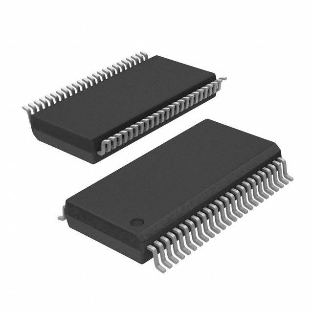
| 描述 | IC BUS BUFF TRI-ST 16BIT 48TSSOP |
| 产品分类 | |
| 品牌 | STMicroelectronics |
| 数据手册 | |
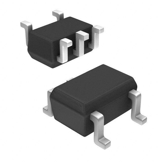
| 产品图片 |
|
| 产品型号 | 74LCX162244TTR |
| rohs | 无铅 / 符合限制有害物质指令(RoHS)规范要求 |
| 产品系列 | 74LCX |
| 产品目录页面 | |
| 供应商器件封装 | 48-TSSOP |
| 元件数 | 4 |
| 其它名称 | 497-1053-1 |
| 包装 | 剪切带 (CT) |
| 安装类型 | 表面贴装 |
| 封装/外壳 | 48-TFSOP(0.240",6.10mm 宽) |
| 工作温度 | -40°C ~ 85°C |
| 标准包装 | 1 |
| 每元件位数 | 4 |
| 电压-电源 | 2 V ~ 3.6 V |
| 电流-输出高,低 | 12mA,12mA |
| 逻辑类型 | 缓冲器/线路驱动器,非反相 |


- 商务部:美国ITC正式对集成电路等产品启动337调查
- 曝三星4nm工艺存在良率问题 高通将骁龙8 Gen1或转产台积电
- 太阳诱电将投资9.5亿元在常州建新厂生产MLCC 预计2023年完工
- 英特尔发布欧洲新工厂建设计划 深化IDM 2.0 战略
- 台积电先进制程称霸业界 有大客户加持明年业绩稳了
- 达到5530亿美元!SIA预计今年全球半导体销售额将创下新高
- 英特尔拟将自动驾驶子公司Mobileye上市 估值或超500亿美元
- 三星加码芯片和SET,合并消费电子和移动部门,撤换高东真等 CEO
- 三星电子宣布重大人事变动 还合并消费电子和移动部门
- 海关总署:前11个月进口集成电路产品价值2.52万亿元 增长14.8%


PDF Datasheet 数据手册内容提取
74LCX162244 LOW VOLTAGE CMOS 16-BIT BUS BUFFER (3-STATE) WITH 5V TOLERANT INPUTS AND OUTPUTS n 5VTOLERANTINPUTSANDOUTPUTS n HIGHSPEED: t =4.4ns (MAX.)atV =3V PD CC n POWERDOWNPROTECTIONONINPUTS ANDOUTPUTS n SYMMETRICALOUTPUTIMPEDANCE: |I |=I =12mA(MIN)atV =3V TSSOP OH OL CC n PCIBUS LEVELS GUARANTEEDAT12mA n BALANCEDPROPAGATIONDELAYS: t @ t ORDERCODES PLH PHL n 26W SERIERESISTORS INOUTPUTS PACKAGE TUBE T&R n OPERATINGVOLTAGERANGE: TSSOP 74LCX162244TTR V (OPR)=2.0Vto3.6V (1.5V Data CC Retention) PINCONNECTION n PINANDFUNCTIONCOMPATIBLE WITH 74SERIES 162244 n LATCH-UPPERFORMANCE EXCEEDS 500mA(JESD17) n ESDPERFORMANCE: HBM >2000V(MILSTD883method3015); MM>200V DESCRIPTION The74LCX162244is alowvoltageCMOS16BIT BUS BUFFER (NON-INVERTED) fabricated with sub-micron silicon gate and double-layer metal wiringC2MOStechnology.Itisidealforlowpower and high speed 3.3V applications; it can be interfacedto5Vsignalenvironmentforbothinputs andoutputs. Any nG output control governs four BUS BUFF- ERS.OutputEnableinput(nG)tiedtogethergives full16-bitoperation. WhennGisLOW,theoutputsareon.WhennGis HIGH,theoutputareinhighimpedancestate. This device is designed to be used with 3 state memoryaddressdrivers,etc. The device circuits is including 26W series resis- tance in theoutputs. Theseresistors permit to re- ducelinenoiseinhighspeedapplications. All inputs and outputs are equipped with protec- tion circuits against static discharge, giving them 2KV ESDimmunityandtransientexcess voltage. February2003 1/10
74LCX162244 INPUTANDOUTPUTEQUIVALENTCIRCUIT PINDESCRIPTION IECLOGICSYMBOLS PINNo SYMBOL NAMEANDFUNCTION 1 1G OutputEnableInput 2,3,5,6 1Y1to1Y4 DataOutputs 8,9,11,12 2Y1to2Y4 DataOutputs 13,14,16,17 3Y1to3Y4 DataOutputs 19,20,22,23 4Y1to4Y4 DataOutputs 24 4G OutputEnableInput 25 3G OutputEnableInput 30,29,27,26 4A1to4A4 DataOutputs 36,35,33,32 3A1to3A4 DataOutputs 41,40,38,37 2A1to2A4 DataOutputs 47,46,44,43 1A1to1A4 DataOutputs 48 2G OutputEnableInput 4,10, 15,21, GND Ground(0V) 28,34,39,45 7,18,31,42 VCC PositiveSupplyVoltage TRUTHTABLE INPUTS OUTPUT G An Yn L L L L H H H X Z X:Don‘tCare Z:HighImpedance 2/10
74LCX162244 ABSOLUTEMAXIMUMRATINGS Symbol Parameter Value Unit VCC SupplyVoltage -0.5to+7.0 V VI DCInputVoltage -0.5to+7.0 V VO DCOutputVoltage(OFFState) -0.5to+7.0 V VO DCOutputVoltage(HighorLowState)(note1) -0.5toVCC+0.5 V IIK DCInputDiodeCurrent -50 mA IOK DCOutputDiodeCurrent(note2) -50 mA IO DCOutputCurrent – 50 mA ICC DCSupplyCurrentperSupplyPin – 100 mA IGND DCGroundCurrentperSupplyPin – 100 mA Tstg StorageTemperature -65to+150 °C TL LeadTemperature(10sec) 300 °C AbsoluteMaximumRatingsarethosevaluesbeyondwhichdamagetothedevicemayoccur.Functionaloperationundertheseconditionsis notimplied 1)I absolutemaximumratingmustbeobserved O 2)V <GND O RECOMMENDEDOPERATINGCONDITIONS Symbol Parameter Value Unit VCC SupplyVoltage(note1) 2.0to3.6 V VI InputVoltage 0to5.5 V VO OutputVoltage(OFFState) 0to5.5 V VO OutputVoltage(HighorLowState) 0toVCC V IOH,IOL HighorLowLevelOutputCurrent(VCC=3.0to3.6V) – 12 mA IOH,IOL HighorLowLevelOutputCurrent(VCC=2.7V) – 8 mA Top OperatingTemperature -55to125 °C dt/dv Input RiseandFallTime(note2) 0to10 ns/V 1)TruthTableguaranteed:1.5Vto3.6V 2)V from0.8Vto2VatV =3.0V IN CC 3/10
74LCX162244 DCSPECIFICATIONS TestCondition Value Symbol Parameter -40to85°C -55to125°C Unit V CC (V) Min. Max. Min. Max. V HighLevelInput IH 2.0 2.0 V Voltage 2.7to3.6 V LowLevelInput IL 0.8 0.8 V Voltage VOH HighLevelOutput 2.7to3.6 IO=-100m A VCC-0.2 VCC-0.2 Voltage 2.7 IO=-8mA 2.0 2.0 V IO=-6mA 2.4 2.4 3.0 IO=-12mA 2.0 2.0 VOL LowLevelOutput 2.7to3.6 IO=100m A 0.2 0.2 Voltage 2.7 IO=8mA 0.6 0.6 V IO=6mA 0.55 0.55 3.0 IO=12mA 0.8 0.8 I InputLeakage I Current 2.7to3.6 VI=0to5.5V – 5 – 5 m A I PowerOffLeakage off Current 0 VIorVO=5.5V 10 10 m A I HighImpedance OZ V =V orV OutputLeakage 2.7to3.6 I IH IL – 5 – 5 m A V =0toV Current O CC ICC QCuurieresnctentSupply 2.7to3.6 VI=VCCorGND 20 20 m A VIorVO=3.6to5.5V – 20 – 20 D ICC ICCincr.perInput 2.7to3.6 VIH=VCC-0.6V 500 500 m A DYNAMICSWITCHINGCHARACTERISTICS TestCondition Value Symbol Parameter V TA=25°C Unit CC (V) Min. Typ. Max. VVOOLLVP DOyuntpaumti(cnLootew1L)evelQuiet 3.3 VIL=C0LV=,V5I0Hp=F3.3V -00..88 V 1)Numberofoutputsdefinedas"n".Measuredwith"n-1"outputsswitchingfromHIGHtoLOWorLOWtoHIGH.Theremainingoutputis measuredintheLOWstate. 4/10
74LCX162244 ACELECTRICALCHARACTERISTICS TestCondition Value Symbol Parameter -40to85°C -55to125°C Unit V C R t =t CC L L s r (V) (pF) (W ) (ns) Min. Max. Min. Max. t t PropagationDelay 2.7 1.5 5.6 1.5 6.5 PLH PHL 50 500 2.5 ns Time 3.0to3.6 1.5 4.4 1.5 5.1 t t OutputEnableTime 2.7 1.5 6.3 1.5 7.2 PZL PZH 50 500 2.5 ns 3.0to3.6 1.5 5.9 1.5 6.8 t t OutputDisableTime 2.7 1.5 6.3 1.5 7.2 PLZ PHZ 50 500 2.5 ns 3.0to3.6 1.5 5.9 1.5 6.8 t OutputToOutput 3.0to3.6 50 500 2.5 1.0 1.0 ns OSLH t SkewTime(note1, OSHL 2) 1)Skewisdefinedastheabsolutevalueofthedifferencebetweentheactualpropagationdelayforanytwooutputsofthesamedeviceswitch- inginthesamedirection,eitherHIGHorLOW(t =|t -t |,t =|t -t |) OSLH PLHm PLHn OSHL PHLm PHLn 2)Parameterguaranteedbydesign CAPACITIVECHARACTERISTICS TestCondition Value Symbol Parameter V TA=25°C Unit CC (V) Min. Typ. Max. CIN InputCapacitance 4 pF COUT OutputCapacitance 10 pF C PowerDissipationCapacitance 3.3 f =10MHz 50 PD IN pF (note1) V =0orV IN CC 1)C isdefinedasthevalueoftheIC’sinternalequivalentcapacitancewhichiscalculatedfromtheoperatingcurrentconsumptionwithout PD load.(RefertoTestCircuit).Averageoperatingcurrentcanbeobtainedbythefollowingequation.I =C xV xf +I /16(per CC(opr) PD CC IN CC circuit) 5/10
74LCX162244 TESTCIRCUIT TEST SWITCH tPLH,tPHL Open t ,t 6V PZL PLZ t ,t GND PZH PHZ C =50pForequivalent(includesjigandprobecapacitance) RL=R1=500W orequivalent RL=Z ofpulsegenerator(typically50W ) T OUT WAVEFORM 1:PROPAGATIONDELAYS(f=1MHz; 50%duty cycle) 6/10
74LCX162244 WAVEFORM 2:OUTPUTENABLEANDDISABLETIME(f=1MHz;50% dutycycle) 7/10
74LCX162244 TSSOP48 MECHANICAL DATA mm. inch DIM. MIN. TYP MAX. MIN. TYP. MAX. A 1.2 0.047 A1 0.05 0.15 0.002 0.006 A2 0.9 0.035 b 0.17 0.27 0.0067 0.011 c 0.09 0.20 0.0035 0.0079 D 12.4 12.6 0.488 0.496 E 8.1 BSC 0.318 BSC E1 6.0 6.2 0.236 0.244 e 0.5 BSC 0.0197 BSC K 0˚ 8˚ 0˚ 8˚ L 0.50 0.75 0.020 0.030 A A2 K L A1 b e c E D E1 PIN 1 IDENTIFICATION 1 7065588C 8/10
74LCX162244 Tape & Reel TSSOP48 MECHANICAL DATA mm. inch DIM. MIN. TYP MAX. MIN. TYP. MAX. A 330 12.992 C 12.8 13.2 0.504 0.519 D 20.2 0.795 N 60 2.362 T 30.4 1.197 Ao 8.7 8.9 0.343 0.350 Bo 13.1 13.3 0.516 0.524 Ko 1.5 1.7 0.059 0.067 Po 3.9 4.1 0.153 0.161 P 11.9 12.1 0.468 0.476 9/10
74LCX162244 Information furnished is believed to be accurate and reliable. However, STMicroelectronics assumes no responsibility for the consequences of use of such information nor for any infringement of patents or other rights of third parties which may result from its use. No license is granted by implication or otherwise under any patent or patent rights of STMicroelectronics. Specifications mentioned in this publication are subject to change without notice. This publication supersedes and replaces all information previously supplied. STMicroelectronics products are not authorized for use as critical components in life support devices or systems without express written approval of STMicroelectronics. © The ST logo is a registered trademark of STMicroelectronics © 2003 STMicroelectronics - Printed in Italy - All Rights Reserved STMicroelectronics GROUP OF COMPANIES Australia - Brazil - Canada - China - Finland - France - Germany - Hong Kong - India - Israel - Italy - Japan - Malaysia - Malta - Morocco Singapore - Spain - Sweden - Switzerland - United Kingdom - United States. © http://www.st.com 10/10