ICGOO在线商城 > 集成电路(IC) > 数据采集 - 数模转换器 > DAC7731E

 Datasheet下载
- 型号: DAC7731E
- 制造商: Texas Instruments
- 库位|库存: xxxx|xxxx
- 要求:
| 数量阶梯 | 香港交货 | 国内含税 |
| +xxxx | $xxxx | ¥xxxx |
查看当月历史价格
查看今年历史价格
DAC7731E产品简介:
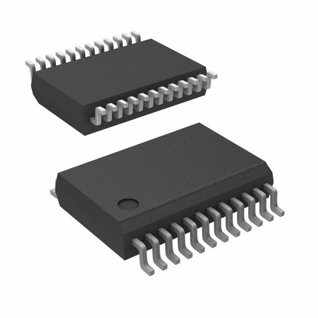
ICGOO电子元器件商城为您提供DAC7731E由Texas Instruments设计生产,在icgoo商城现货销售,并且可以通过原厂、代理商等渠道进行代购。 DAC7731E价格参考。Texas InstrumentsDAC7731E封装/规格:数据采集 - 数模转换器, 16 位 数模转换器 1 24-SSOP。您可以下载DAC7731E参考资料、Datasheet数据手册功能说明书,资料中有DAC7731E 详细功能的应用电路图电压和使用方法及教程。
Texas Instruments(德州仪器)的DAC7731E是一款单通道、低功耗、16位数字-模拟转换器(DAC),广泛应用于需要高精度和低功耗的数据采集系统中。以下是其主要应用场景:

1. 工业自动化与控制
   DAC7731E可用于工业自动化中的精密信号生成,例如调节传感器输出或控制执行器的动作。其16位分辨率和低功耗特性使其适合用于远程控制系统或电池供电的设备。

2. 医疗设备
   在医疗领域,该芯片可用于便携式医疗设备中,如血压监测仪、血糖仪或便携式超声设备。这些设备通常需要精确的信号生成和低功耗设计,而DAC7731E能够满足这些需求。

3. 测试与测量设备
   该DAC可以用于测试仪器中,例如信号发生器或数据记录仪。它能够提供高精度的电压输出,以校准或模拟各种测试条件。

4. 通信系统
   在通信领域,DAC7731E可用于生成精确的模拟信号,例如调整功率放大器的偏置电压或生成参考信号。其小尺寸和低功耗特性非常适合便携式或嵌入式通信设备。

5. 消费电子
   在一些高端消费电子产品中,DAC7731E可以用于音频信号处理、触摸屏校准或背光调节等场景,提供更高的精度和稳定性。

6. 汽车电子
   该芯片适用于汽车电子中的传感器校准或信号调节应用,例如胎压监测系统(TPMS)或环境传感器。其低功耗特性有助于减少车辆电池的负担。

7. 可编程电源和伺服控制
   DAC7731E可用于可编程电源或伺服控制系统中,生成精确的参考电压或控制信号,从而实现对电机速度、位置或扭矩的精准控制。

总之,DAC7731E凭借其高精度、低功耗和紧凑封装的特点,非常适合需要高性能和小型化设计的应用场景。
| 参数 | 数值 |
| 产品目录 | 集成电路 (IC)半导体 |
| 描述 | IC D/A CONV LP 16-BIT 24-SSOP数模转换器- DAC 16-Bit Sng Ch W/Int +10V Ref & Ser I/F |
| 产品分类 | |
| 品牌 | Texas Instruments |
| 产品手册 | http://www.ti.com/litv/sbas249b |
| 产品图片 |
|
| rohs | 符合RoHS无铅 / 符合限制有害物质指令(RoHS)规范要求 |
| 产品系列 | 数据转换器IC,数模转换器- DAC,Texas Instruments DAC7731E- |
| 数据手册 | |
| 产品型号 | DAC7731E |
| PCN组件/产地 | |
| 产品培训模块 | http://www.digikey.cn/PTM/IndividualPTM.page?site=cn&lang=zhs&ptm=13240 |
| 产品种类 | 数模转换器- DAC |
| 位数 | 16 |
| 供应商器件封装 | 24-SSOP |
| 其它名称 | 296-33256-5 |
| 分辨率 | 16 bit |
| 制造商产品页 | http://www.ti.com/general/docs/suppproductinfo.tsp?distId=10&orderablePartNumber=DAC7731E |
| 包装 | 管件 |
| 商标 | Texas Instruments |
| 安装类型 | 表面贴装 |
| 安装风格 | SMD/SMT |
| 封装 | Tube |
| 封装/外壳 | 24-SSOP(0.209",5.30mm 宽) |
| 封装/箱体 | SSOP-24 |
| 工作温度 | -40°C ~ 85°C |
| 工厂包装数量 | 60 |
| 建立时间 | 3µs |
| 接口类型 | Serial (3-Wire, SPI) |
| 数据接口 | SPI |
| 最大功率耗散 | 150 mW |
| 最大工作温度 | + 85 C |
| 最小工作温度 | - 40 C |
| 标准包装 | 60 |
| 电压参考 | Internal or External |
| 电压源 | 模拟和数字,双 ± |
| 电源电压-最大 | 5.25 V, 15.75 V |
| 电源电压-最小 | 4.75 V, 11.4 V |
| 积分非线性 | 6 LSB |
| 稳定时间 | 5 us |
| 系列 | DAC7731 |
| 结构 | R-2R |
| 转换器数 | 1 |
| 转换器数量 | 1 |
| 输出数和类型 | 1 电压,单极1 电压,双极 |
| 输出类型 | Voltage Buffered |
| 配用 | /product-detail/zh/5-6KINTERFACE/296-18350-ND/561912/product-detail/zh/DAC7731EVM/296-19939-ND/562103 |
| 采样比 | 172 kSPs |
| 采样率(每秒) | - |


PDF Datasheet 数据手册内容提取
DAC7731 DAC7731 SBAS249B – DECEMBER 2001 – REVISED NOVEMBER 2007 16-Bit, Voltage Output, Serial Input DIGITAL-TO-ANALOG CONVERTER FEATURES DESCRIPTION (cid:1) LOW POWER: 150mW MAXIMUM The DAC7731 is a 16-bit Digital-to-Analog Converter (DAC) (cid:1) +10V INTERNAL REFERENCE which provides 16 bits of monotonic performance over the (cid:1) UNIPOLAR OR BIPOLAR OPERATION specified operating temperature range and offers a +10V internal reference. Designed for automatic test equipment (cid:1) SETTLING TIME: 5µs to ±0.003% FSR and industrial process control applications, the DAC7731 (cid:1) 16-BIT MONOTONICITY, –40°C TO +85°C output swing can be configured in a ±10V, ±5V, or +10V (cid:1) ±10V, ±5V, OR +10V CONFIGURABLE VOLTAGE range. The flexibility of the output configuration allows the OUTPUT DAC7731 to provide both unipolar and bipolar operation by (cid:1) RESET TO ZERO OR MID-SCALE pin strapping. The DAC7731 includes a high-speed output (cid:1) DOUBLE-BUFFERED DATA INPUT amplifier with a maximum settling time of 5µs to ±0.003% (cid:1) DAISY-CHAIN FEATURE FOR MULTIPLE FSR for a 20V full-scale change and only consumes 100mW (typical) of power. DAC7731s ON A SINGLE BUS (cid:1) SMALL SSOP-24 PACKAGE The DAC7731 features a standard 3-wire, SPI-compatible serial interface with double buffering to allow asynchronous updates of the analog output as well as a serial data output APPLICATIONS line for daisy-chaining multiple DAC7731s. A user program- (cid:1) PROCESS CONTROL mable reset control forces the DAC output to either min-scale (cid:1) ATE PIN ELECTRONICS (0000h) or mid-scale (8000h), overriding both the input and DAC register values. The DAC7731 is available in a (cid:1) CLOSED-LOOP SERVO CONTROL SSOP-24 package and three performance grades specified (cid:1) MOTOR CONTROL to operate from –40°C to +85°C. (cid:1) DATA ACQUISITION SYSTEMS VDD VSS VCC REFADJ REFOUT REFIN VREF R OFFSET Buffer REFEN RFB2 +10V RSTSEL Reference RST Control LDAC Logic RFB1 SCLK CS SJ SDO Enable Input DAC DAC SDI Register Register V OUT AGND DGND Please be aware that an important notice concerning availability, standard warranty, and use in critical applications of Texas Instruments semiconductor products and disclaimers thereto appears at the end of this data sheet. All trademarks are the property of their respective owners. PRODUCTION DATA information is current as of publication date. Copyright © 2001-2007, Texas Instruments Incorporated Products conform to specifications per the terms of Texas Instruments standard warranty. Production processing does not necessarily include testing of all parameters. www.ti.com
ABSOLUTE MAXIMUM RATINGS(1) ELECTROSTATIC V to V ...........................................................................–0.3V to +32V DISCHARGE SENSITIVITY CC SS V to AGND......................................................................–0.3V to +16V CC V to AGND......................................................................–16V to +0.3V SS This integrated circuit can be damaged by ESD. Texas Instru- AGNDto DGND...................................................................–0.3V to 0.3V REF to AGND..............................................................0V to V –1.4V ments recommends that all integrated circuits be handled with IN CC VDD to DGND........................................................................–0.3V to +6V appropriate precautions. Failure to observe proper handling Digital Input Voltage to DGND.................................–0.3V to V + 0.3V DD and installation procedures can cause damage. Digital Output Voltage to DGND..............................–0.3V to V + 0.3V DD Operating Temperature Range........................................–40°C to +85°C ESD damage can range from subtle performance degradation Storage Temperature Range.........................................–65°C to +150°C Junction Temperature (TJ Max)....................................................+150°C to complete device failure. Precision integrated circuits may be more susceptible to damage because very small parametric NOTE: (1) Stresses above those listed under Absolute Maximum Ratings may changes could cause the device not to meet its published cause permanent damage to the device. Exposure to absolute maximum conditions for extended periods may affect device reliability. specifications. PACKAGE/ORDERING INFORMATION(1) SPECIFIED PACKAGE TEMPERATURE PACKAGE ORDERING TRANSPORT PRODUCT PACKAGE-LEAD DESIGNATOR RANGE MARKING NUMBER(2) MEDIA, QUANTITY DAC7731E SSOP-24 DB –40°C to +85°C DAC7731E DAC7731E Rails, 60 " " " " " DAC7731E/1K Tape and Reel,1000 DAC7731EB SSOP-24 DB –40°C to +85°C DAC7731EB DAC7731EB Rails, 60 " " " " " DAC7731EB/1K Tape and Reel, 1000 DAC7731EC SSOP-24 DB –40°C to +85°C DAC7731EC DAC7731EC Rails, 60 " " " " " DAC7731EC/1K Tape and Reel, 1000 NOTE: (1) For the most current package ordering information, see the Package Option Addendum at the end of this data sheet, or see the TI web site at www.ti.com. PIN CONFIGURATION PIN DESCRIPTIONS Top View SSOP PIN NAME DESCRIPTION 1 V Positive Analog Power Supply CC 2 REF Internal Reference Output OUT 3 REF Reference Input IN 4 REFADJ Internal Reference Trim. (Acts as a gain adjustment input when the internal reference is used.) 5 V Buffered Output from REF , can be used to drive REF IN external devices. Internally, this pin directly drives the V 1 24 V DAC's circuitry. CC SS 6 R Offsetting Resistor OFFSET REF 2 23 REFEN 7 AGND Analog ground OUT 8 RFB2 Feedback Resistor 2, used to configure DAC output REFIN 3 22 RSTSEL range. 9 RFB1 Feedback Resistor 1, used to configure DAC output REFADJ 4 21 SCLK range. 10 SJ Summing Junction of the Output Amplifier V 5 20 CS REF 11 V DAC Voltage Output OUT ROFFSET 6 19 SDO 12 VDD Digital Power Supply DAC7731 13 DGND Digital Ground AGND 7 18 SDI 14 TEST Reserved, Connect to DGND 15 NC No Connection RFB2 8 17 LDAC 16 RST V reset; active LOW, depending on the state of OUT RSTSEL, the DAC register is either reset to mid- RFB1 9 16 RST scale or min-scale. SJ 10 15 NC 17 LDAC DAC register load control, rising dege triggered. Data is loaded from the input register to the DAC register. V 11 14 TEST 18 SDI Serial Data Input. Data is latched into the input OUT register on the rising edge of SCLK. VDD 12 13 DGND 19 SDO Serial Data Output, delayed 16 SCLK clock cycles. 20 CS Chip Select, Active LOW 21 SCLK Serial Clock Input 22 RSTSEL Reset Select; determines the action of RST. If HIGH, RST will reset the DAC register to mid-scale. If LOW, RST will reset the DAC register to min-scale. 23 REFEN Enables internal +10V reference (REF ), active OUT NOTE: RST, LDAC, SDI, CS and SCK are Schmitt-triggered inputs. LOW. 24 V Negative Analog Power Supply SS DAC7731 2 www.ti.com SBAS249B
ELECTRICAL CHARACTERISTICS All specifications at T = T to T , V = +15V, V = –15V, V = +5V, Internal refi⁄ence enabled, unless otherwise noted. A MIN MAX CC SS DD DAC7731E DAC7731EB DAC7731EC PARAMETER CONDITIONS MIN TYP MAX MIN TYP MAX MIN TYP MAX UNITS ACCURACY Linearity Error (INL) ±6 ±4 ±3 LSB T = 25°C ±5 ±3 ±2 LSB A Differential Linearity Error (DNL) ±4 ±2 ±1 LSB Monotonicity 14 15 16 Bits Offset Error ±0.1 ✻ ✻ % of FSR Offset Error Drift ±2 ✻ ✻ ppm/°C Gain Error With Internal REF ±0.4 ±0.25 ±0.15 % of FSR With External REF ±0.25 ±0.1 ✻ % of FSR Gain Error Drift With Internal REF ±15 ±10 ±7 ppm/°C PSRR (V or V ) At Full-Scale 50 200 ✻ ✻ ✻ ✻ ppm/V CC SS ANALOG OUTPUT(1) Voltage Output(2) +11.4/–4.75 0 to 10 ✻ ✻ V +11.4/–11.4 ±10 ✻ ✻ V +11.4/–6.4 ±5 ✻ ✻ V Output Current ±5 ✻ ✻ mA Output Impeadance 0.1 ✻ ✻ Ω Maximum Load Capacitance 200 ✻ ✻ pF Short-Circuit Current ±15 ✻ ✻ mA Short-Circuit Duration AGND Indefinite ✻ ✻ REFERENCE Reference Output 9.96 10 10.04 9.975 ✻ 10.025 ✻ ✻ ✻ V REF Impedance 400 ✻ ✻ Ω OUT REF Voltage Drift ±15 ±10 ±7 ppm/°C OUT REF Voltage Adjustment(3) ±25 ✻ ✻ mV OUT REF Input Range(4) 4.75 V – 1.4 ✻ ✻ ✻ ✻ V IN CC REF Input Current 10 ✻ ✻ nA IN REFADJ Input Range Absolute Max Value that 0 10 ✻ ✻ ✻ ✻ V can be applied is V CC REFADJ Input Impedance 50 ✻ ✻ kΩ V Output Current –2 +2 ✻ ✻ ✻ ✻ mA REF V Impedance 1 ✻ ✻ Ω REF DYNAMIC PERFORMANCE Settling Time to ±0.003% 20V Output Step 3 5 ✻ ✻ ✻ ✻ µs R = 5kΩ, C = 200pF, L L with external REF OUT to REF filter(5) IN Digital Feedthrough 2 ✻ ✻ nV-s Output Noise Voltage at 10kHz 100 ✻ ✻ nV/√Hz DIGITAL INPUT V |I | < 10µA 0.7 • V ✻ ✻ V IH H DD V |I| < 10µA 0.3 • V ✻ ✻ V IL L DD DIGITAL OUTPUT V I = –0.8mA 3.6 ✻ ✻ V OH OH V I = 1.6mA 0.4 ✻ ✻ V OL OL POWER SUPPLY V +4.75 +5.0 +5.25 ✻ ✻ ✻ ✻ ✻ ✻ V DD V +11.4 +15.75 ✻ ✻ ✻ ✻ V CC V Bipolar Operation –15.75 –11.4 ✻ ✻ ✻ ✻ V SS Unipolar Opeation –15.75 –4.75 ✻ ✻ ✻ ✻ V I 100 ✻ ✻ µA DD I Unloaded 4 6 ✻ ✻ ✻ ✻ mA CC I Unloaded –4 –2.5 ✻ ✻ ✻ ✻ mA SS Power No Load, Ext. Reference 85 ✻ ✻ mW No Load, Int. Reference 100 150 ✻ ✻ ✻ ✻ mW TEMPERATURE RANGE Specified Performance –40 +85 ✻ ✻ ✻ ✻ °C ✻ Specifications same as grade to the left. NOTES:(1)With minimum V /V requirements, internal reference enabled. CC SS (2)Please refer to the Theory of Operation section for more information with respect to output voltage configurations. (3)See Figure 11 for gain and offset adjustment connection diagrams when using the internal reference. (4)The minimum value for REF must be equal to the greater of V +14V and +4.75V, where +4.75V is the minimum voltage allowed. IN SS (5)Reference low-pass filter values: 100kΩ, 1.0µF (see Figure 14). DAC7731 3 SBAS249B www.ti.com
TIMING CHARACTERISTICS V = +15V, V = –15V, V = 5V; R = 2kΩ to AGND; C = 200pF to AGND; all specifications –40°C to +85°C, unless otherwise noted. CC SS DD L L DAC7731 PARAMETER DESCRIPTION MIN TYP MAX UNITS t SCLK HIGH Time 25 ns WH t SCLK LOW Time 25 ns WL t Setup Time: Data in valid before rising SCLK 5 ns SDI t Hold Time: Data in valid after rising SCLK 20 ns HDI t Setup Time: CS falling edge before first rising SCLK 15 ns SCS t Hold Time: CS rising edge after 16th rising SCLK 0 ns HSC t Delay Time: CS Falling Edge to Data Out valid, C = 20pF on SDO 50 ns DDO L t Hold Time: Data Out valid after SCLK rising edge, C 20pF on SDO 50 ns HDO L t Delay Time: CS rising edge to SDO = High Impedance 70 ns DDOZ t CS HIGH Time 50 ns WCSH t LDAC LOW Time 20 ns WLDL t LDAC HIGH Time 20 ns WLDH t Setup Time: 16th Rising SCLK Before LDAC Rising Edge 15 ns SLD t Delay Time: LDAC rising edge to first SCLK rising edge of next 15 ns DLD transfer cycle. t Setup Time: CS High before falling SCLK edge following 16th 5 ns SCLK rising SCLK edge t Setup Time: RSTSEL Valid Before RST LOW 0 ns SRS t Hold Time: RSTSEL valid after RST HIGH 20 ns HRS t RST LOW Time 30 ns WRL t DAC V Settling Time 5 µs S OUT INTERFACE TIMING tSCS tHCS CS tWCSH t WH SCLK 1 2 16 t t t WL SCLK t HDI SDI B15 B14 B13 B0 C15 C14 C13 C12 SDI tDDO Word B Word C t t HDO DDOZ A15 A14 A13 A0 B15 B14 B13 B12 SDO t DLD Word A tWLDL Word B LDAC tWLDH tSLD tS V OUT ±0.003% of FSR Error Bands RESET TIMING t SRS RSTSEL t HRS RST tWRL +FS tS (RSTSEL = LOW) VOUT Min-Scale –FS +FS Mid-Scale V (RSTSEL = HIGH) OUT –FS DAC7731 4 www.ti.com SBAS249B
TYPICAL CHARACTERISTICS T = +25°C (unless otherwise noted). A LINEARITY ERROR AND DIFFERENTIAL LINEARITY ERROR AND DIFFERENTIAL LINEARITY ERROR vs DIGITAL INPUT CODE LINEARITY ERROR vs DIGITAL INPUT CODE 6 6 4 4 SB) 2 SB) 2 INL (L –––0246 BTAip =o la8r5 °CCo,n Ifnigteurrnaatilo Rn:e VfeOreUTn c=e – E1n0aVb tleod +10V INL (L –––0246 BTAip =o la2r5 °CCo,n Ifnigteurrnaatilo Rn:e VfeOreUTn c=e –E1n0aVb tleod +10V 2.0 2.0 1.5 1.5 B) 1.0 B) 1.0 NL (LS –000...505 NL (LS –000...505 D –1.0 D –1.0 –1.5 –1.5 –2.0 –2.0 0000H 2000H 4000H 6000H 8000H A000HC000H E000HFFFFH 0000H 2000H 4000H 6000H 8000H A000HC000H E000HFFFFH Digital Input Code Digital Input Code LINEARITY ERROR AND DIFFERENTIAL LINEARITY ERROR vs DIGITAL INPUT CODE OFFSET ERROR vs TEMPERATURE 6 1.00 4 INL (LSB) –––24620 BTAip =o la–r4 0C°oCn,f iIgnuterarntiaoln R: VefOeUrTe n=c –e1 E0nVa tbole +d10V mV) 000...752505 VOUT = 0 to +10V VOUT = –10 to +10V 21..05 Error ( –00..0205 B) 1.0 S 0.5 –0.50 L NL ( –00..05 –0.75 D –1.0 –1.5 –2.0 –1.00 0000 2000 4000 6000 8000 A000 C000 E000 FFFF –40 –15 10 35 60 85 H H H H H H H H H Temperature (°C) Digital Input Code GAIN ERROR vs TEMPERATURE VCC SUPPLY CURRENT vs DIGITAL INPUT CODE 0.000 4.4 Bipolar Configuration: V = –10V to +10V OUT –0.010 Internal Reference Enabled, T = 25°C Ext. Ref, Unipolar Mode: V = 0 to +10V 4.3 A –0.020 OUT –0.030 4.2 Ext. Ref, Bipolar Mode: V = –10 to +10V %) –0.040 Int. Ref, Unipolar Mode: V = 0 to +1O0UVT A) 4.1 Error ( ––00..005600 OUT (mCC 4.0 I –0.070 3.9 –0.080 –0.090 Int. Ref, Bipolar Mode: VOUT = –10 to +10V 3.8 Load = 200pF, 2kΩ –0.100 3.7 –40 –15 10 35 60 85 0000 2000 4000 6000 8000 A000 C000 E000 FFFF H H H H H H H H H Temperature (°C) Digital Input Code DAC7731 5 SBAS249B www.ti.com
TYPICAL CHARACTERISTICS (Cont.) T = +25°C (unless otherwise noted). A V SUPPLY CURRENT vs DIGITAL INPUT CODE V SUPPLY CURRENT vs DIGITAL INPUT CODE CC SS 3.4 –1.50 Bipolar Configuration: V = –10V to +10V OUT External Reference, REFEN = 5V, T = 25°C 3.3 A –1.75 3.2 –2.00 A) 3.1 A) m m (CC 3.0 (SS –2.25 I I 2.9 –2.50 2.8 Bipolar Configuration: VOUT = –10V to +10V T = 25°C A 2.7 –2.75 0000 2000 4000 6000 8000 A000 C000 E000 FFFF 0000 2000 4000 6000 8000 A000 C000 E000 FFFF H H H H H H H H H H H H H H H H H H Digital Input Code Digital Input Code SUPPLY CURRENT vs TEMPERATURE SUPPLY CURRENT vs LOGIC INPUT VOLTAGE 7 1800 Load Current Excluded T = 25°C, Transition 6 V = +15V, V = –15V 1600 SAhown for a Single CC SS 5 Bipolar VOUT Configuration: –10V to +10V 1400 Input (Applies to CS, SCLK,D and LDAC 4 1200 inputs) IN (mA)SS 32 ICC µ (A)D1080000 , IC 1 ID C 600 I 0 400 –1 I SS 200 –2 –3 0 –40 –15 10 35 60 85 0.0 0.5 1.0 1.5 2.0 2.5 3.0 3.5 4.0 4.5 5.0 Temperature (°C) VLOGIC (V) 100 HISTOGRAM OF VCC CURRENT CONSUMPTION 100 HISTOGRAM OF VSS CURRENT CONSUMPTION Bipolar Output Configuration Bipolar Output Configuration 90 Internal Reference Enabled 90 Internal Reference Enabled 80 Code = 5555H 80 Code = 5555H 70 70 Frequency 654000 Frequency 654000 30 30 20 20 10 10 0 0 3.000 3.500 4.000 4.500 5.000 –3.50 –3.00 –2.50 –2.00 –1.50 ICC (mA) ISS (mA) DAC7731 6 www.ti.com SBAS249B
TYPICAL CHARACTERISTICS (Cont.) T = +25°C (unless otherwise noted). A POWER-SUPPY REJECTION RATIO vs FREQUENCY POWER-SUPPY REJECTION RATIO vs FREQUENCY 10 (Measured at VOUT) 10 (Measured at VOUT) 0 BCiopdoela 8r 0C0o0nHfiguration: ±10V VOUT 0 B–VipSoSl,a Vr CCCo n=f i1g5uVra +ti o1nV: p±-1p0, VV DVDO =UT 5, VC o+d 0e. 5FVFpF-FpH –10 –VSS, VCC = 15V + 1Vp-p –10 V = 5V + 0.5Vp-p –20 DD –20 V RR (dB) ––3400 RR (dB) ––3400 SS VCC PS –50 VSS PS –50 –60 VCC –60 VDD –70 –70 V –80 DD –80 0.1K 1K 10K 100K 1M 10M 0.01K 0.1K 1K 10K 100K 1M 10M Frequency (Hz) Frequency (Hz) INTERNAL REFERENCE OUTPUT vs TEMPERATURE INTERNAL REFERENCE START-UP 10.015 v)15V 10.010 di V/ 5 (C 0V 10.005 VC V) (UT 10.000 O F div) 10V RE 9.995 V/ 2 (UT 9.990 O F RE 0V 9.985 –40 –15 10 35 60 85 Time (2ms/div) Temperature (°C) 11.0 REFOUT VOLTAGE vs LOAD 12 OUTPUT VOLTAGE vs RLOAD Source Loaded to VCC VCC = +15V 8 10.5 4 EF (V)OUT 109..50 V (V)OUT 0 R –4 Sink 9.0 –8 Loaded to AGND 8.5 –12 1 10 100 1K 0.0 0.1 1.0 10.0 100.0 REFOUT LOAD(kΩ) RLOAD (kΩ) DAC7731 7 SBAS249B www.ti.com
TYPICAL CHARACTERISTICS (Cont.) T = +25°C (unless otherwise noted). A POWER-SUPPY REJECTION RATIO vs FREQUENCY (Measured at REF ) OUT OUTPUT NOISE vs FREQUENCY 10 900 Internal Reference Enabled Unipolar Configuration, Internal Reference Enabled 0 –VSS, VCC = 15V + 1Vp-p, 800 V = 5V + 0.5Vp-p –10 DD 700 z) RR (dB) –––234000 VCC Noise (nV/H 654000000 Code FFFFH PS VSS VDD ut –50 p 300 ut O –60 200 Code 0000 –70 100 H –80 0 1 10 100 1K 10K 100K 1M 10M 0.01K 0.1K 1K 10K 100K 1M 10M Frequency (Hz) Frequency (Hz) OUTPUT NOISE vs FREQUENCY BROADBAND NOISE 800 Bipolar Configuration: ±10V, Internal Reference Enabled 700 z) 600 nV/rtH 500 V/div) se ( 400 µ50 Noi Code 0000H V, utput 300 Code FFFFH V (OUT Internal Reference Enabled O 200 Code 8000 Filtered with 1.6Hz Low-Pass 100 H Code FFFFH, Bipolar ±10V Configuration 10kHz Measurement BW 0 0.01K 0.1K 1K 10K 100K 1M 10M Time (100µs/div) Frequency (Hz) UNIPOLAR FULL-SCALE SETTLING TIME BIPOLAR FULL-SCALE SETTLING TIME Large-Signal Output (5V/div) Large-Signal Output (5V/div) Small-Signal Error (150µV/div) Small-Signal Error (300µV/div) Unipolar Configuration: VOUT = 0 to +10V Bipolar Configuration: VOUT = –10 to +10V Zero-Scale to +Full-Scale Change –Full-Scale to +Full-Scale 5kΩ, 200pF Load 5kΩ, 200pF Load Time (2µs/div) Time (2µs/div) DAC7731 8 www.ti.com SBAS249B
TYPICAL CHARACTERISTICS (Cont.) T = +25°C (unless otherwise noted). A UNIPOLAR FULL-SCALE SETTLING TIME BIPOLAR FULL-SCALE SETTLING TIME Small-Signal Error (150µV/div) Small-Signal Error (300µV/div) Large-Signal Output (5V/div) Large-Signal Output (5V/div) Unipolar Configuration: VOUT = 0V to +10V Bipolar Configuration: VOUT = –10 to +10V +Full-Scale to Zero-Scale Change +Full-Scale to –Full-Scale 5kΩ, 200pF Load 5kΩ, 200pF Load Time (2µs/div) Time (2µs/div) MID-SCALE GLITCH MID-SCALE GLITCH Code 8000 to 7FFF Code 7FFF to 8000 H H H H Bipolar Configuration: ±10V V Bipolar Configuration: ±10V V OUT OUT div) div) V/ V/ m m 0 0 0 0 1 1 V, V, (OUT (OUT V V Time (1µs/div) Time (1µs/div) DAC7731 9 SBAS249B www.ti.com
THEORY OF OPERATION The digital input is a serial word made up of the DAC code (MSB first) and is loaded into the DAC register using the The DAC7731 is a voltage output, 16-bit DAC with a +10V LDAC input pin. The converter can be powered from ±12V built-in internal reference. The architecture is an R-2R ladder to ±15V dual analog supplies and a +5V logic supply. The configuration with the three MSBs segmented, followed by device offers a reset function, which immediately sets the an operational amplifier that serves as a buffer, as shown in DAC output voltage and DAC register to min-scale (code Figure 1. The output buffer is designed to allow user- 0000 ) or mid-scale (code 8000 ). The data I/O and reset H H configurable output adjustments giving the DAC7731 output functions are discussed in more detail in the following sec- voltage ranges of 0V to +10V, –5V to +5V, or –10V to +10V. tions. Please refer to Figures 2, 3, and 4 for pin configuration information. REFADJ REFOUT REFIN VREF ROFFSET RFB2 Buffer R/4 RFB1 +10V Internal R/2 R/2 R/4 Reference SJ R V OUT 2R 2R 2R 2R 2R 2R 2R 2R 2R R/4 V REF AGND FIGURE 1. DAC7731 Architecture. V V CC CC DAC7731 DAC7731 0.1µF 1µF VSS 0.1µF 1µF VSS 1 VCC VSS 24 1 VCC VSS 24 2 REFOUT REFEN 23 1µF 0.1µF 2 REFOUT REFEN 23 1µF 0.1µF 3 REFIN RSTSEL 22 3 REFIN RSTSEL 22 4 REFADJ SCLK 21 4 REFADJ SCLK 21 5 VREF CS 20 5 VREF CS 20 6 ROFFSET SDO 19 CBuosntrol/Data 6 ROFFSET SDO 19 CBuosntrol/Data 7 AGND SDI 18 7 AGND SDI 18 8 RFB2 LDAC 17 8 RFB2 LDAC 17 9 RFB1 RST 16 9 RFB1 RST 16 10 SJ NC 15 10 SJ NC 15 11 VOUT TEST 14 (–5V to +5V) 11 VOUT TEST 14 (0V to +10V) VDD 12 VDD DGND 13 VDD 12 VDD DGND 13 0.1µF 1µF 0.1µF 1µF FIGURE 2. Basic Operation: V = 0V to +10V. FIGURE 3. Basic Operation: V = –5V to +5V. OUT OUT DAC7731 10 www.ti.com SBAS249B
DAC7731 output amplifier into one of three voltage output V CC modes as discussed earlier. V can also be used to drive DAC7731 REF 0.1µF 1µF VSS other system components requiring an external reference. 1 VCC VSS 24 2 REFOUT REFEN 23 1µF 0.1µF REFEN ACTION 3 REFIN RSTSEL 22 1 Internal Reference disabled; 4 REFADJ SCLK 21 REFOUT = High Impedance 5 VREF CS 20 0 Internal Reference enabled; REF = +10V Control/Data OUT 6 ROFFSET SDO 19 Bus TABLE I. REFEN Action. 7 AGND SDI 18 8 RFB2 LDAC 17 The internal reference of the DAC7731 can be disabled when 9 RFB1 RST 16 use of an external reference is desired. When using an 10 SJ NC 15 external reference, the reference input, REF , can be any IN (–10V to +10V) 11 VOUT TEST 14 voltage between 4.75V (or V + 14V, whichever is greater) SS VDD 12 VDD DGND 13 and VCC – 1.4V. 0.1µF 1µF DIGITAL INTERFACE Table II shows the input data format for the DAC7731 and FIGURE 4. Basic Operation: V = –10V to +10V. Table III illustrates the basic control logic of the device. The OUT serial interface consists of a chip select input (CS), serial data clock input (SCLK), serial data input (SDI), serial data output ANALOG OUTPUTS (SDO), and load control input (LDAC). An asynchronous reset The output amplifier can swing to within 1.4V of the supply input (RST), which is active LOW, is provided to simplify start- rails, specified over the –40°C to +85°C temperature range. up conditions, periodic resets, or emergency resets to a known This allows for a ±10V DAC voltage output operation from state, depending on the status of the reset select (RSTSEL) ±12V supplies with a typical 5% tolerance. signal. Please refer to the DAC Reset section for additional When the DAC7731 is configured for a unipolar, 0V to 10V information regarding the reset operation. output, a negative voltage supply is required. This is due to internal biasing of the output stage. Please refer to the ANALOG OUTPUT Electrical Characteristics table (see page 3) for more infor- DIGITAL INPUT Unipolar Configuration Bipolar Configuration mation. Unipolar Straight Binary Bipolar Offset Binary The minimum and maximum voltage output values are de- 0x0000 Zero (0V) –Full-Scale (–V or –V /2) REF REF pendent upon the output configuration implemented and 0x0001 Zero + 1LSB –Full-Scale + 1LSB reference voltage applied to the DAC7731. Please note that : : : V (the negative power supply) must be in the range of 0x8000 1/2 Full-Scale Bipolar Zero SS 0x8001 1/2 Full-Scale + 1LSB Bipolar Zero + 1LSB –4.75V to –15.75V for unipolar operation. The voltage on V SS : : : sets several bias points within the converter and is required 0xFFFF Full-Scale (V – 1LSB) +Full-Scale (+V – 1LSB in all modes of operation. If V is not in one of these two REF REF SS or +V /2 – 1LSB) configurations, the bias values may be in error and proper REF TABLE II. DAC7731 Data Format. operation of the device is not ensured. Supply sequence is important in establishing the correct startup of the DAC. The following supply sequence must be CONTROL STATUS COMMAND followed: V (device substrate) first, then V followed by CS RSTRSTSEL LDAC SCLK ACTION SS DD H H X X X Shift Register is disabled on the serial bus. V . In addition, each supply must reach the values specified CC Enable SDO pin from High Impedance; in the Electrical Characteristics table (see page 3) within L H X X X enables shift operation and I/O bus 100ms of its ramp start. (SCLK, SDI, SDO). L H X X ↑ Serial Data Shifted into Input Register ↑ H X X L Serial Data Shifted into Input Register(1) REFERENCE INPUTS X H X ↑ X Data in Input Register is Loaded into DAC Register. The DAC7731 provides a built-in +10V voltage reference and X L H X X Resets Input and DAC Registers to mid-scale. on-chip buffer to allow external component reference drive. To X L L X X Resets Input and DAC Registers to min-scale. use the internal reference, REFEN must be LOW, enabling the NOTE: (1) In order to avoid unwanted shifting of the input register by an reference circuitry of the DAC7731 (as shown in Table I) and additional bit, care must be taken that a rising edge on CS only occurs when SCLK is HIGH. the REF pin must be connected to REF . This is the input OUT IN TABLE III. DAC7731 Logic Truth Table. to the on-chip reference buffer. The buffer output is provided at the V pin. In this configuration, V is used to setup the REF REF DAC7731 11 SBAS249B www.ti.com
The DAC code is provided via a 16-bit serial interface, as shown TIMING CONSIDERATIONS in Table II. The digital input word makes up the digital code to The flexible interface of the DAC7731 can operate under a be loaded into the data input register of the device. A typical number of different scenarios as is required by a host data transfer and DAC output update take place as follows: controller. Critical timing for a 16-bit data transfer cycle is Once CS is active (LOW), the DAC7731 is enabled on the serial shown in the Interface Timing section of the Timing Charac- bus and the 16-bit serial data transfer can begin. The serial data teristics. While this is the most common method of writing to is shifted into the device on each rising SCLK edge until all 16 the DAC7731, the device accepts two additional modes of bits are transferred (1 bit per 1 rising SCLK edge). Once data transfer from the host. These are byte transfer mode received, the data in the input register is loaded into the DAC and continuous transfer mode. register upon reception of a rising edge on the LDAC input (load Byte transfer mode is especially useful when an 8-bit host is command). This action updates the analog output, V , to the OUT communicating with the DAC. Data transfer can occur with- desired voltage specified by the digital input word. A rising edge out requiring an additional general purpose I/O pin to control on LDAC is completely asynchronous to the serial interface of the CS input of the DAC in cycles of 16 clocks. A HIGH state the device and can occur at any time. Care must be taken to on CS stops data from coming into and out of the internal ensure that the entire 16 bits of data are loaded into the input shift register. This provides byte-wide support for 8-bit host register before issuing a LDAC active edge. Additional load processors. Figure 5 is an example of the timing cycle of commands will have no effect on the DAC output if the data in such a data transfer. the input register is unchanged between rising LDAC edges. When CS is returned HIGH, the rising edge on CS must The remaining data transfer mode accepted by the DAC7731 occur when SCLK is HIGH. Application of a rising CS edge is continuous transfer. The CS of the DAC7731 can be tied when SCLK is LOW will cause one additional shift in the LOW or held LOW by the controller for an indefinite number of serial input shift register, corrupting the desired input data. serial clock cycles. Each clock cycle will transfer data into the 16-Bit Data Word Most Significant Byte Least Significant Byte CS SCLK 1 2 8 9 10 16 B15 B14 B13 B8 B7 B6 B0 SDI Byte 1, Word N Byte 2, Word N SDO A15 A14 A13 A8 A7 A6 A0 Byte 1, Word N – 1 Byte 2, Word N – 1 LDAC FIGURE 5. Byte-Wide Data Write Cycle. CS SCLK 1 2 16 1 2 16 1 2 SDI B15 B14 B1 B0 C15 C14 C1 C0 D15 D14 Word N Word N + 1 Word N + 2 SDO A15 A14 A1 A0 B15 B14 B1 B0 C15 C14 Word N – 1 Word N Word N + 1 LDAC FIGURE 6. Continuous Transfer Control. DAC7731 12 www.ti.com SBAS249B
DAC via SDI and out of the DAC on SDO. Care must be taken cycle written into the chain will arrive at the last DAC7731 on that the LDAC signal to the DAC(s) is timed correctly so that the final cycle of the data transfer. Upon completion of the valid data is transferred into the DAC register on each rising required number of data transfer cycles (one cycle per LDAC edge. (Valid data refers to the serial data latched on device), each DAC voltage output is updated with a rising each of the 16 rising SCLK edges prior to the occurrence of a edge on the LDAC inputs. Figure 7 shows the required timing rising LDAC signal.) The rising edge of LDAC must occur to properly update two DAC7731s in a daisy-chained con- before the first rising SCLK edge of the following 16-bit figuration, as shown in Figure 8. transfer. Figure 6 shows continuous transfer timing. DAC RESET DAISY-CHAINING USING SDO The RST and RSTSEL inputs control the reset of the analog Multiple DAC7731s can be connected to a single serial port output. The reset command is level triggered by a low signal on by attaching each of their control inputs in parallel and daisy- RST. Once RST is LOW, the DAC output will begin settling to chaining the SDO and SDI I/Os of each device. The SDO the mid-scale or min-scale code depending on the state of the output of the DAC7731 is active when CS is LOW and can RSTSEL input. A HIGH value on RSTSEL will cause V to be left unconnected when not required for use in a daisy- OUT reset to the mid-scale code (8000 ) and a LOW value will reset chain configuration. H V to min-scale (8000 ). A change in the state of the RSTSEL OUT H Once a data transfer cycle begins, new data is shifted into input while RST is LOW will cause a corresponding change in SDI and data currently residing in the shift register (from the reset command selected internally and consequently change previous cycle, power-up, or reset command) is presented the output value of V of the DAC. Note that a valid reset OUT on SDO, MSB first. One data transfer cycle for each DAC7731 signal also resets the input register of the DAC to the value is required to update all devices in the chain. The first data specified by the state of RSTSEL. Both DAC VOUT's are updated LSBs latched LSBs latched SCLK 1 2 16 1 2 16 CS LDAC First Data Transfer Cycle SDI A15 A14 A0 B15 B14 B1 B0 Previous cycle word from host (to DAC7731 B SDI) SDO X X X A15 A14 A1 A0 FIGURE 7. DAC7731 Daisy-Chain Timing for Figure 7. From Host Controller To next DAC7731 DAC7731 DAC7731 1 VCC VSS 24 1 VCC VSS 24 2 REFOUT REFEN 23 2 REFOUT REFEN 23 3 REFIN RSTSEL 22 3 REFIN RSTSEL 22 4 REFADJ SCLK 21 4 REFADJ SCLK 21 5 VREF CS 20 5 VREF CS 20 6 ROFFSET SDO 19 6 ROFFSET SDO 19 7 AGND SDI 18 7 AGND SDI 18 8 RFB2 LDAC 17 8 RFB2 LDAC 17 9 RFB1 RST 16 9 RFB1 RST 16 10 SJ NC 15 10 SJ NC 15 11 VOUT TEST 14 11 VOUT TEST 14 12 VDD DGND 13 12 VDD DGND 13 First Device in Chain Second Device in Chain FIGURE 8. DAC7731 Daisy-Chain Schematic. DAC7731 13 SBAS249B www.ti.com
APPLICATIONS at +10V – 1LSB for the 0V to +10V or ±10V output range and +5V – 1LSB for the ±5V output range. Figure 11 shows the GAIN AND OFFSET CALIBRATION generalized external offset and gain adjustment circuitry The architecture of the DAC7731 is designed in such a way using potentiometers. as to allow for easily configurable offset and gain calibration using a minimum of external components. The DAC7731 has built-in feedback resistors and output amplifier summing points brought out of the package in order to make the absolute calibration possible. Figures 9 and 10 illustrate the DAC7731 relationship of offset and gain adjustments for the DAC7731 irne sap eucntiivpeollya.r configuration and in a bipolar configuration, OptiAodnjauls Gtain EFADJ REF OFFSET GND FB2 FB1 J R V R A R R S R POT1 4 5 6 7 8 9 10 (+V ) Optional Offset REF Adjust ISJ + Full Scale Gain Adjust 1LSB Rotates (Other Cofonrn Ceclatiroitnys) Omitted R1 Output Range the Line RPOT2 + RS g e VOADJ o al – nal Sc A ull Input = F 0000 H Input = FFFF FIGURE 11. Generalized External Calibration Circuitry for H Gain and Symmetrical Offset Adjustment. Zero Scale (AGND) Digital Input OFFSET ADJUSTMENT Offset Adjust Translates the Line Offset adjustment is accomplished by introducing a small FIGURE 9. Relationship of Offset and Gain Adjustments for current into the summing junction (SJ) of the DAC7731. The VOUT = 0V to +10V Output Configuration. voltage at SJ, or VSJ, is dependent on the output configura- tion of the DAC7731. See Table IV for the required pin strapping for a given configuration and the nominal values of (+VREF or +VREF/2) VSJ for each output range. + Full Scale REFERENCE OUTPUT PIN STRAPPING V (1) SJ 1LSB CONFIGURATION CONFIGURATION R RFB1 RFB2 OFFSET Input = Internal 0V to +10V to V to V to V +5V 0000 e Gain REF OUT OUT H calge Adjust Reference –10V to +10V NC NC to VOUT +3.333V Sn –5V to +5V to AGND to V to V +1.666V Output Full Ra tRhoet aLtinees OAdffjsuestt ERxetfeerrneanlce –V0RVE tFo t oV RVERFEF to NVCREF to NVCOOUUTT ttoo VVOOOUUUTTT VVRREEFF//23 og Translates –VREF/2 to VREF/2 to AGND to VOUT to VOUT VREF/6 Anal Input = the Line NOTE: (1) Voltage measured at VSJ for a given configuration. Input = 8000 FFFF H TABLE IV. Nominal VSJ versus VOUT and Reference Configu- H ration. – Full-Scale (–V OR –V /2) The current level required to adjust the DAC7731’s offset can REF REF be created by using a potentiometer divider as shown in Digital Input Figure 11 Another alternative is to use a unipolar DAC in order FIGURE 10. Relationship of Offset and Gain Adjustments for to apply a voltage, V , to the resistor R . A ±2uA current OADJ S V = –10V to +10V Output Configuration. (Same range applied to SJ will ensure offset adjustment coverage of OUT Theory Applies for V = –5V to +5V.) the ±0.1% maximum offset specification of the DAC7731. OUT When in a unipolar configuration (V = 5V), only a single SJ When calibrating the DAC output, offset should be adjusted resistor, RS, is needed for symmetrical offset adjustment with first to avoid first order interaction of adjustments. In unipolar a 0V to 10V VOADJ range. When in one of the two bipolar mode, the DAC7731 offset is adjusted from code 0000H and configurations, VSJ is either +3.333V (±10V range) or +1.666V for either bipolar mode, offset adjustments are made at code (±5V range), and circuit values chosen to match those given 8000 . Gain adjustment can then be made at code FFFF for in Table V will provide symmetrical offset adjust. Please refer H H each configuration, where the output of the DAC should be to Figure 11 for component configuration. DAC7731 14 www.ti.com SBAS249B
OUTPUT R R R I NOMINAL POT2 1 S SJ CONFIGURATION RANGE OFFSET ADJUSTMENT REFOUT ADJUST RANGE 40 0V to +10V 10K 0 2.5M ±2µA ±25mV –10V to +10V 10K 5K 1.5M ±2.2µA ±55mV 30 Typical REFOUT –5V to +5V 10K 20K 1M ±1.7µA ±21mV V) Adjustment Range m 20 TABLE V. Recommended External Component Values for nt ( e 10 Symmetrical Offset Adjustment (V = 10V). m REF Adjust 0 AMdijnuismtmumen Rt ERFaOnUgTe UT –10 Figure 12 illustrates the typical minimum offset adjustment FO E –20 ranges provided by forcing a current at SJ for a given output R voltage configuration. –30 –40 0 2 4 6 8 10 REFADJ (V) OFFSET ADJUST RANGE 50 typ –10V to +10V VOUT FIGURE 13. Internal Reference Adjustment Transfer Charac- V) Configuration teristic. m min (75% of typ) (T 25 U O V at typ VOLTAGE AT REFADJ REFOUT VOLTAGE ent 0 REFADJ = 0V 10V + 25mV (min) m REFADJ = 5V or NC(1) 10V ust min (75% of typ) REFADJ = 10V 10V – 25mV (max) Offset Adj –25 0VVOU tTo C10oVnf iagnudra –ti5oVn to +5V TNAOBTLE:E N CV I=. NMoitn Cimonunemct eIdn.ternal Reference Adjustment Range. –50 –2 –1 0 1 2 NOISE PERFORMANCE I (µA) Increased noise performance of the DAC output can be SJ achieved by filtering the voltage reference input to the DAC7731. Figure 14 shows a typical internal reference filter schematic. A FIGURE 12. Offset Adjustment Transfer Characteristic. low-pass filter applied between the REF and REF pins can OUT IN increase noise immunity at the DAC and output amplifier. The GAIN ADJUSTMENT REFOUT pin can source a maximum of 50µA so care should be taken in order to avoid overloading the internal reference output. When using the internal reference of the DAC7731, gain adjustment is performed by adjusting the device’s internal reference voltage via the reference adjust pin, REFADJ. The DAC7731 effect of a reference voltage change on the gain of the DAC output can be seen in the generic equation (for unipolar 1 V V 24 Low-Pass Reference Filter CC SS configuration): 2 REF REFEN 23 OUT VOUT = VREFIN • (N/65536) 1.0µF 100kΩ 3 REF RSTSEL 22 Where N is represented in decimal format and ranges from IN 0 to 65535. 4 REFADJ SCLK 21 REFADJ can be driven by a low impedance voltage source 5 V CS 20 REF such as a unipolar, 0V to +10V DAC or a potentiometer (less 6 R SDO 19 OFFSET than 100kΩ), see Figure 11. Since the input impedance of REFADJ is typically 50kΩ, the smaller the resistance of the 7 AGND SDI 18 potentiometer, the more linear the adjustment will be. A 10kΩ 8 RFB2 LDAC 17 potentiometer is suggested if linearity of the reference adjust- 9 RFB1 RST 16 ment is of concern. 10 SJ NC 15 When the DAC7731’s internal reference is not used, gain adjustments can be made via trimming the external refer- 11 VOUT TEST 14 ence applied to the DAC at REFIN. This can be accomplished 12 VDD DGND 13 through using a potentiometer, unipolar DAC, or other means of precision voltage adjustment to control the voltage pre- (Other connections omitted for clarity.) sented to the DAC7731 by the external reference. Figure 13 and Table VI summarize the range of adjustment of the FIGURE 14. Filtering the Internal Reference. internal reference via REFADJ. DAC7731 15 SBAS249B www.ti.com
LAYOUT The voltages applied to V and V should be well regulated CC SS and low noise. Switching power supplies and DC/DC convert- A precision analog component requires careful layout, adequate ers will often have high-frequency glitches or spikes riding on bypassing, and clean, well-regulated power supplies. The the output voltage. In addition, digital components can create DAC7731 offers separate digital and analog supplies, as it will similar high-frequency spikes as their internal logic switches often be used in close proximity with digital logic, microcontrollers, states. This noise can easily couple into the DAC output microprocessors, and digital signal processors. The more digital voltage through various paths between the power connec- logic present in the design and the higher the switching speed, tions and analog output. the more important it will become to separate the analog and In addition, a 1µF to 10µF bypass capacitor in parallel with a digital ground and supply planes at the device. 0.1µF bypass capacitor is strongly recommended for each Since the DAC7731 has both analog and digital ground pins, supply input. In some situations, additional bypassing may be return currents can be better controlled and have less effect required, such as a 100µF electrolytic capacitor or even a Pi on the DAC output error. Ideally, AGND would be connected filter made up of inductors and capacitors–all designed to directly to an analog ground plane and DGND to the digital essentially low-pass filter the analog supplies, removing any ground plane. The analog ground plane would be separate high frequency noise components. from the ground connection for the digital components until they were connected at the power-entry point of the system. DAC7731 16 www.ti.com SBAS249B
PACKAGE OPTION ADDENDUM www.ti.com 6-Feb-2020 PACKAGING INFORMATION Orderable Device Status Package Type Package Pins Package Eco Plan Lead/Ball Finish MSL Peak Temp Op Temp (°C) Device Marking Samples (1) Drawing Qty (2) (6) (3) (4/5) DAC7731E ACTIVE SSOP DB 24 60 Green (RoHS NIPDAU Level-3-260C-168 HR -40 to 85 DAC7731E & no Sb/Br) DAC7731E/1K ACTIVE SSOP DB 24 1000 Green (RoHS NIPDAU Level-3-260C-168 HR -40 to 85 DAC7731E & no Sb/Br) DAC7731EB ACTIVE SSOP DB 24 60 Green (RoHS NIPDAU Level-3-260C-168 HR -40 to 85 DAC7731E & no Sb/Br) B DAC7731EB/1K ACTIVE SSOP DB 24 1000 Green (RoHS NIPDAU Level-3-260C-168 HR -40 to 85 DAC7731E & no Sb/Br) B DAC7731EC ACTIVE SSOP DB 24 60 Green (RoHS NIPDAU Level-3-260C-168 HR -40 to 85 DAC7731E & no Sb/Br) C DAC7731EC/1K ACTIVE SSOP DB 24 1000 Green (RoHS NIPDAU Level-3-260C-168 HR -40 to 85 DAC7731E & no Sb/Br) C DAC7731ECG4 ACTIVE SSOP DB 24 60 Green (RoHS NIPDAU Level-3-260C-168 HR -40 to 85 DAC7731E & no Sb/Br) C (1) The marketing status values are defined as follows: ACTIVE: Product device recommended for new designs. LIFEBUY: TI has announced that the device will be discontinued, and a lifetime-buy period is in effect. NRND: Not recommended for new designs. Device is in production to support existing customers, but TI does not recommend using this part in a new design. PREVIEW: Device has been announced but is not in production. Samples may or may not be available. OBSOLETE: TI has discontinued the production of the device. (2) RoHS: TI defines "RoHS" to mean semiconductor products that are compliant with the current EU RoHS requirements for all 10 RoHS substances, including the requirement that RoHS substance do not exceed 0.1% by weight in homogeneous materials. Where designed to be soldered at high temperatures, "RoHS" products are suitable for use in specified lead-free processes. TI may reference these types of products as "Pb-Free". RoHS Exempt: TI defines "RoHS Exempt" to mean products that contain lead but are compliant with EU RoHS pursuant to a specific EU RoHS exemption. Green: TI defines "Green" to mean the content of Chlorine (Cl) and Bromine (Br) based flame retardants meet JS709B low halogen requirements of <=1000ppm threshold. Antimony trioxide based flame retardants must also meet the <=1000ppm threshold requirement. (3) MSL, Peak Temp. - The Moisture Sensitivity Level rating according to the JEDEC industry standard classifications, and peak solder temperature. (4) There may be additional marking, which relates to the logo, the lot trace code information, or the environmental category on the device. (5) Multiple Device Markings will be inside parentheses. Only one Device Marking contained in parentheses and separated by a "~" will appear on a device. If a line is indented then it is a continuation of the previous line and the two combined represent the entire Device Marking for that device. Addendum-Page 1
PACKAGE OPTION ADDENDUM www.ti.com 6-Feb-2020 (6) Lead/Ball Finish - Orderable Devices may have multiple material finish options. Finish options are separated by a vertical ruled line. Lead/Ball Finish values may wrap to two lines if the finish value exceeds the maximum column width. Important Information and Disclaimer:The information provided on this page represents TI's knowledge and belief as of the date that it is provided. TI bases its knowledge and belief on information provided by third parties, and makes no representation or warranty as to the accuracy of such information. Efforts are underway to better integrate information from third parties. TI has taken and continues to take reasonable steps to provide representative and accurate information but may not have conducted destructive testing or chemical analysis on incoming materials and chemicals. TI and TI suppliers consider certain information to be proprietary, and thus CAS numbers and other limited information may not be available for release. In no event shall TI's liability arising out of such information exceed the total purchase price of the TI part(s) at issue in this document sold by TI to Customer on an annual basis. Addendum-Page 2
PACKAGE MATERIALS INFORMATION www.ti.com 14-Jul-2012 TAPE AND REEL INFORMATION *Alldimensionsarenominal Device Package Package Pins SPQ Reel Reel A0 B0 K0 P1 W Pin1 Type Drawing Diameter Width (mm) (mm) (mm) (mm) (mm) Quadrant (mm) W1(mm) DAC7731E/1K SSOP DB 24 1000 330.0 16.4 8.2 8.8 2.5 12.0 16.0 Q1 DAC7731EB/1K SSOP DB 24 1000 330.0 16.4 8.2 8.8 2.5 12.0 16.0 Q1 DAC7731EC/1K SSOP DB 24 1000 330.0 16.4 8.2 8.8 2.5 12.0 16.0 Q1 PackMaterials-Page1
PACKAGE MATERIALS INFORMATION www.ti.com 14-Jul-2012 *Alldimensionsarenominal Device PackageType PackageDrawing Pins SPQ Length(mm) Width(mm) Height(mm) DAC7731E/1K SSOP DB 24 1000 367.0 367.0 38.0 DAC7731EB/1K SSOP DB 24 1000 367.0 367.0 38.0 DAC7731EC/1K SSOP DB 24 1000 367.0 367.0 38.0 PackMaterials-Page2
MECHANICAL DATA MSSO002E – JANUARY 1995 – REVISED DECEMBER 2001 DB (R-PDSO-G**) PLASTIC SMALL-OUTLINE 28 PINS SHOWN 0,38 0,65 0,15 M 0,22 28 15 0,25 0,09 5,60 8,20 5,00 7,40 Gage Plane 1 14 0,25 A 0°–(cid:1)8° 0,95 0,55 Seating Plane 2,00 MAX 0,05 MIN 0,10 PINS ** 14 16 20 24 28 30 38 DIM A MAX 6,50 6,50 7,50 8,50 10,50 10,50 12,90 A MIN 5,90 5,90 6,90 7,90 9,90 9,90 12,30 4040065/E 12/01 NOTES: A. All linear dimensions are in millimeters. B. This drawing is subject to change without notice. C. Body dimensions do not include mold flash or protrusion not to exceed 0,15. D. Falls within JEDEC MO-150 • POST OFFICE BOX 655303 DALLAS, TEXAS 75265
IMPORTANTNOTICEANDDISCLAIMER TI PROVIDES TECHNICAL AND RELIABILITY DATA (INCLUDING DATASHEETS), DESIGN RESOURCES (INCLUDING REFERENCE DESIGNS), APPLICATION OR OTHER DESIGN ADVICE, WEB TOOLS, SAFETY INFORMATION, AND OTHER RESOURCES “AS IS” AND WITH ALL FAULTS, AND DISCLAIMS ALL WARRANTIES, EXPRESS AND IMPLIED, INCLUDING WITHOUT LIMITATION ANY IMPLIED WARRANTIES OF MERCHANTABILITY, FITNESS FOR A PARTICULAR PURPOSE OR NON-INFRINGEMENT OF THIRD PARTY INTELLECTUAL PROPERTY RIGHTS. These resources are intended for skilled developers designing with TI products. You are solely responsible for (1) selecting the appropriate TI products for your application, (2) designing, validating and testing your application, and (3) ensuring your application meets applicable standards, and any other safety, security, or other requirements. These resources are subject to change without notice. TI grants you permission to use these resources only for development of an application that uses the TI products described in the resource. Other reproduction and display of these resources is prohibited. No license is granted to any other TI intellectual property right or to any third party intellectual property right. TI disclaims responsibility for, and you will fully indemnify TI and its representatives against, any claims, damages, costs, losses, and liabilities arising out of your use of these resources. TI’s products are provided subject to TI’s Terms of Sale (www.ti.com/legal/termsofsale.html) or other applicable terms available either on ti.com or provided in conjunction with such TI products. TI’s provision of these resources does not expand or otherwise alter TI’s applicable warranties or warranty disclaimers for TI products. Mailing Address: Texas Instruments, Post Office Box 655303, Dallas, Texas 75265 Copyright © 2020, Texas Instruments Incorporated