ICGOO在线商城 > 集成电路(IC) > 数据采集 - 数模转换器 > AD5546CRUZ

 Datasheet下载
- 型号: AD5546CRUZ
- 制造商: Analog
- 库位|库存: xxxx|xxxx
- 要求:
| 数量阶梯 | 香港交货 | 国内含税 |
| +xxxx | $xxxx | ¥xxxx |
查看当月历史价格
查看今年历史价格
AD5546CRUZ产品简介:
ICGOO电子元器件商城为您提供AD5546CRUZ由Analog设计生产,在icgoo商城现货销售,并且可以通过原厂、代理商等渠道进行代购。 AD5546CRUZ价格参考。AnalogAD5546CRUZ封装/规格:数据采集 - 数模转换器, 16 位 数模转换器 1 28-TSSOP。您可以下载AD5546CRUZ参考资料、Datasheet数据手册功能说明书,资料中有AD5546CRUZ 详细功能的应用电路图电压和使用方法及教程。
AD5546CRUZ是Analog Devices Inc.(ADI公司)生产的一款高精度、低功耗的16位数模转换器(DAC),属于数据采集系统中的关键组件。它广泛应用于需要高分辨率和高稳定性的模拟信号输出场景,特别适合工业控制、测试测量、通信系统、医疗设备以及音频处理等领域。

在工业控制系统中,AD5546CRUZ可以用于精密调节和控制各种参数,如温度、压力、流量等。其高分辨率确保了对这些物理量的精确控制,而低功耗特性则有助于减少系统能耗,提高整体效率。此外,该器件还支持多种供电电压范围,使其能够适应不同的工业环境需求。

在测试与测量仪器中,AD5546CRUZ可用于生成精确的参考电压或电流源,为校准和其他精密测量任务提供可靠的基准信号。由于其优异的线性度和低噪声性能,使得测试结果更加准确可靠。

对于通信系统而言,AD5546CRUZ可以在发射端产生高质量的调制波形,以实现更清晰稳定的传输效果;同时,在接收端也可以用来恢复原始信号,保证数据传输的质量。

在医疗设备方面,这款DAC可用于心电图机、超声波成像仪等仪器中,负责将数字信号转换成模拟信号进行显示或进一步处理。其高精度和稳定性对于确保诊断结果的准确性至关重要。

总之,AD5546CRUZ凭借其出色的性能指标,在众多领域内发挥着重要作用,为用户提供了一个高性能且灵活的选择方案。
| 参数 | 数值 |
| 产品目录 | 集成电路 (IC)半导体 |
| 描述 | IC DAC 16BIT PAR 28TSSOP数模转换器- DAC 16-Bit Parallel Current Outpt IC |
| DevelopmentKit | EVAL-AD5546SDZ |
| 产品分类 | |
| 品牌 | Analog Devices |
| 产品手册 | |
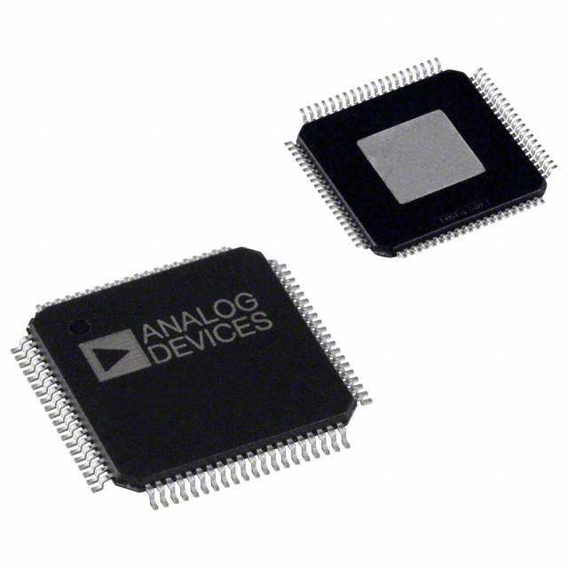
| 产品图片 |
|
| rohs | 符合RoHS无铅 / 符合限制有害物质指令(RoHS)规范要求 |
| 产品系列 | 数据转换器IC,数模转换器- DAC,Analog Devices AD5546CRUZ- |
| 数据手册 | |
| 产品型号 | AD5546CRUZ |
| 产品培训模块 | http://www.digikey.cn/PTM/IndividualPTM.page?site=cn&lang=zhs&ptm=26125http://www.digikey.cn/PTM/IndividualPTM.page?site=cn&lang=zhs&ptm=26140http://www.digikey.cn/PTM/IndividualPTM.page?site=cn&lang=zhs&ptm=26150http://www.digikey.cn/PTM/IndividualPTM.page?site=cn&lang=zhs&ptm=26146http://www.digikey.cn/PTM/IndividualPTM.page?site=cn&lang=zhs&ptm=26147 |
| 产品目录页面 | |
| 产品种类 | 数模转换器- DAC |
| 位数 | 16 |
| 供应商器件封装 | 28-TSSOP |
| 分辨率 | 16 bit |
| 包装 | 管件 |
| 商标 | Analog Devices |
| 安装类型 | 表面贴装 |
| 安装风格 | SMD/SMT |
| 封装 | Tube |
| 封装/外壳 | 28-TSSOP(0.173",4.40mm 宽) |
| 封装/箱体 | TSSOP-28 |
| 工作温度 | -40°C ~ 125°C |
| 工厂包装数量 | 50 |
| 建立时间 | 500ns |
| 接口类型 | Parallel |
| 数据接口 | 并联 |
| 最大功率耗散 | 55 uW |
| 最大工作温度 | + 125 C |
| 最小工作温度 | - 40 C |
| 标准包装 | 1 |
| 电压参考 | External |
| 电压源 | 单电源 |
| 电源电压-最大 | 5.5 V |
| 电源电压-最小 | 2.7 V |
| 积分非线性 | +/- 1 LSB |
| 稳定时间 | 500 ns |
| 系列 | AD5546 |
| 结构 | R-2R, Current Steering |
| 视频文件 | http://www.digikey.jp/classic/video.aspx?PlayerID=1364138032001&width=640&height=505&videoID= 2389427697001 |
| 设计资源 | 点击此处下载产品Datasheet点击此处下载产品Datasheet点击此处下载产品Datasheet点击此处下载产品Datasheet |
| 转换器数 | 1 |
| 转换器数量 | 1 |
| 输出数和类型 | 1 电流,单极1 电流,双极 |
| 输出类型 | Current |
| 采样比 | 2 MSPs |
| 采样率(每秒) | 2M |


- 商务部:美国ITC正式对集成电路等产品启动337调查
- 曝三星4nm工艺存在良率问题 高通将骁龙8 Gen1或转产台积电
- 太阳诱电将投资9.5亿元在常州建新厂生产MLCC 预计2023年完工
- 英特尔发布欧洲新工厂建设计划 深化IDM 2.0 战略
- 台积电先进制程称霸业界 有大客户加持明年业绩稳了
- 达到5530亿美元!SIA预计今年全球半导体销售额将创下新高
- 英特尔拟将自动驾驶子公司Mobileye上市 估值或超500亿美元
- 三星加码芯片和SET,合并消费电子和移动部门,撤换高东真等 CEO
- 三星电子宣布重大人事变动 还合并消费电子和移动部门
- 海关总署:前11个月进口集成电路产品价值2.52万亿元 增长14.8%


PDF Datasheet 数据手册内容提取
Current Output, Parallel Input, 16-/14-Bit Multiplying DACs with Four-Quadrant Resistors Data Sheet AD5546/AD5556 FEATURES FUNCTIONAL BLOCK DIAGRAM 16-bit resolution R1 RCOM REF ROFS 14-bit resolution R1 R2 ROFS RFB 2- or 4-quadrant multiplying DAC RFB ±±11 LLSSBB DINNLL VDD AADD55554566/ DAC IOUT 16/14 Operating supply voltage: 2.7 V to 5.5 V WR Low noise: 12 nV/√Hz COLNOTGRICOL DAC LDAC REGISTER Low power: IDD = 10 μA DB0TO DB15 GND 0.5 μs settling time Built-in R facilitates current-to-voltage conversion POR FB Buoilrt -±in1 04 -Vq ouuatdpruantst resistors allow 0 V to –10 V, 0 V to +10 V, MSB RS 03810-001 2 mA full-scale current ±20%, with V = 10 V Figure 1. AD5546/AD5556 Simplified Block Diagram REF Automotive operating temperature: –40°C to +125°C GENERAL DESCRIPTION Compact TSSOP-28 package The AD5546/AD5556 are precision 16-/14-bit, multiplying, low APPLICATIONS power, current output, parallel input digital-to-analog converters (DACs). They operate from a single 2.7 V to 5.5 V supply with Automatic test equipment ±10 V multiplying references for four-quadrant outputs. Built- Instrumentation in four-quadrant resistors facilitate the resistance matching and Digitally controlled calibration Digital waveform generation temperature tracking that minimize the number of components needed for multiquadrant applications. The feedback resistor (R ) simplifies the I-V conversion with an external buffer. The FB AD5546/AD5556 are packaged in compact TSSOP-28 packages with operating temperatures from –40°C to +125°C. The EVAL-AD5546SDZ is available for evaluating DAC perfor- mance. For more information, see the UG-309 evaluation board user guide. + U2A OP2177 – +10V C7 –10V R1A RCOMA VREFA ROFSA RFBA +15V C4 C6 1µF R1 R2 ROFS RFB +5V VDD 1CµF1 0.1CµF2 16-/14-BIT IOUT – 0.C15µF U1 DATA V+ AD5546/AD5556 U2B OP2177 VOUT GND V– 16-/14-BIT + DATA C8 1µF WR LDAC RS MSB WR C9 LMDARSCBS –15V0.1µF 03810-024 Figure 2. 16-/14-Bit, Four-Quadrant Multiplying DAC with a Minimum of External Components R ev. D Information furnished by Analog Devices is believed to be accurate and reliable. However, no responsibility is assumed by Analog Devices for its use, nor for any infringements of patents or other One Technology Way, P.O. Box 9106, Norwood, MA 02062-9106, U.S.A. rights of third parties that may result from its use. Specifications subject to change without notice. No license is granted by implication or otherwise under any patent or patent rights of Analog Devices. Tel: 781.329.4700 www.analog.com Trademarks and registered trademarks are the property of their respective owners. Fax: 781.461.3113 ©2004-2011 Analog Devices, Inc. All rights reserved.
AD5546/AD5556 Data Sheet TABLE OF CONTENTS Features .............................................................................................. 1 Digital Section ............................................................................ 11 Applications ....................................................................................... 1 ESD Protection Circuits ............................................................ 11 Functional Block Diagram .............................................................. 1 Amplifier Selection .................................................................... 11 General Description ......................................................................... 1 Reference Selection .................................................................... 11 Revision History ............................................................................... 2 Applications Information .............................................................. 12 Specifications ..................................................................................... 3 Unipolar Mode ........................................................................... 12 Electrical Characteristics ............................................................. 3 Bipolar Mode .............................................................................. 13 Timing Diagram ........................................................................... 4 AC Reference Signal Attenuator ............................................... 14 Absolute Maximum Ratings ............................................................ 5 System Calibration ..................................................................... 14 ESD Caution .................................................................................. 5 Reference Selection .................................................................... 15 Pin Configurations and Function Descriptions ........................... 6 Amplifier Selection .................................................................... 15 Typical Performance Characteristics ............................................. 8 Outline Dimensions ....................................................................... 17 Circuit Operation ........................................................................... 10 Ordering Guide .......................................................................... 17 Digital-to-Analog (DAC) Converter Section ......................... 10 REVISION HISTORY 11/11—Rev. C to Rev. D Changes to General Description Section ...................................... 1 Changes to Ordering Guide .......................................................... 18 1/11—Rev. B to Rev. C Changes to Figure 2 .......................................................................... 1 Changes to Figure 21 ...................................................................... 13 4/10—Rev. A to Rev. B Changes to Table 1 ............................................................................ 4 Moved Timing Diagram Section and Figure 5 to Specifications Section....................................................................... 4 Moved Table 5 Through Table 7 to Digital Section Section ....... 7 Replaced Figure 15 and Figure 16 .................................................. 9 Deleted Figure 17 and Figure 18 ..................................................... 9 Added Reference Selection Section, Amplifier Selection Section, and Table 11 Through Table 13 .................................................... 15 9/09—Rev. 0 to Rev. A Changes to Features Section............................................................ 1 Changes to Static Performance, Relative Accuracy, Grade: AD5546C Parameter, Table 1 ............................................. 3 Changes to Ordering Guide .......................................................... 16 1/04—Revision 0: Initial Version Rev. D | Page 2 of 20
Data Sheet AD5546/AD5556 SPECIFICATIONS ELECTRICAL CHARACTERISTICS V = 2.7 V to 5.5 V, I = virtual GND, GND = 0 V, V = –10 V to 10 V, T = full operating temperature range, unless otherwise noted. DD OUT REF A Table 1. Parameter Symbol Conditions Min Typ Max Unit STATIC PERFORMANCE1 Resolution N AD5546, 1 LSB = V /216 = 153 µV at 16 Bits REF V = 10 V REF AD5556, 1 LSB = V /214 = 610 µV at 14 Bits REF V = 10 V REF Relative Accuracy INL Grade: AD5556C ±1 LSB Grade: AD5546B ±2 LSB Grade: AD5546C ±1 LSB Differential Nonlinearity DNL Monotonic ±1 LSB Output Leakage Current I Data = zero scale, T = 25°C 10 nA OUT A Data = zero scale, T = T maximum 20 nA A A Full-Scale Gain Error G Data = full scale ±1 ±4 mV FSE Bipolar Mode Gain Error G Data = full scale ±1 ±4 mV E Bipolar Mode Zero-Scale G Data = full scale ±1 ±2.5 mV ZSE Error Full-Scale Tempco2 TCV 1 ppm/°C FS REFERENCE INPUT V Range V –18 +18 V REF REF REF Input Resistance REF 4 5 6 kΩ R1 and R2 Resistance R1 and R2 4 5 6 kΩ R1-to-R2 Mismatch ∆(R1 to R2) ±0.5 ±1.5 Ω Feedback and Offset RFB, ROFS 8 10 12 kΩ Resistance Input Capacitance2 C 5 pF REF ANALOG OUTPUT Output Current I Data = full scale 2 mA OUT Output Capacitance2 C Code dependent 200 pF OUT LOGIC INPUT AND OUTPUT Logic Input Low Voltage V V = 5 V 0.8 V IL DD V = 3 V 0.4 V DD Logic Input High Voltage V V = 5 V 2.4 V IH DD V = 3 V 2.1 V DD Input Leakage Current I 10 µA IL Input Capacitance2 C 10 pF IL INTERFACE TIMING2, 3 Data to WR Setup Time tDS VDD = 5 V 20 ns V = 3 V 35 ns DD Data to WR Hold Time tDH VDD = 5 V 0 ns V = 3 V 0 ns DD WR Pulse Width tWR VDD = 5 V 20 ns V = 3 V 35 ns DD LDAC Pulse Width t V = 5 V 20 ns LDAC DD V = 3 V 35 ns DD Rev. D | Page 3 of 20
AD5546/AD5556 Data Sheet Parameter Symbol Conditions Min Typ Max Unit RS Pulse Width t V = 5 V 20 ns RS DD V = 3 V 35 ns DD WR to LDAC Delay Time t V = 5 V 0 ns LWD DD V = 3 V 0 ns DD SUPPLY CHARACTERISTICS Power Supply Range V 2.7 5.5 V DD RANGE Positive Supply Current I Logic inputs = 0 V 10 μA DD Power Dissipation P Logic inputs = 0 V 0.055 mW DISS Power Supply Sensitivity P ∆V = ±5% 0.003 %/% SS DD AC CHARACTERISTICS4 Output Voltage Settling t To ±0.1% of full scale, data cycles from zero 0.5 μs S Time scale to full scale to zero scale Reference Multiplying BW BW V = 100 mV rms, data = full scale, C6 =5.6 pF5 6.8 MHz REF DAC Glitch Impulse Q V = 0 V, midscale minus 1 to midscale −3 nV-s REF Multiplying Feedthrough V /V V = 100 mV rms, f = 10 kHz 79 dB OUT REF REF Error Digital Feedthrough Q WR = 1, LDAC toggles at 1 MHz 7 nV-s D Total Harmonic Distortion THD V = 5 V p-p, data = full-scale, f = 1 kHz –103 dB REF Output Noise Density e f = 1 kHz, BW = 1 Hz 12 nV/rt Hz N 1 All static performance tests (except IOUT) are performed in a closed-loop system, using an external precision OP97 I-V converter amplifier. The AD554x RFB terminal is tied to the amplifier output. The op amp +IN is grounded, and the DAC IOUT is tied to the op amp –IN. Typical values represent average readings measured at 25°C. 2 These parameters are guaranteed by design and are not subject to production testing. 3 All input control signals are specified with tR = tF = 2.5 ns (10% to 90% of 3 V) and timed from a voltage level of 1.5 V. 4 All ac characteristic tests are performed in a closed-loop system using an AD8038 I-V converter amplifier except for THD where an AD8065 was used. 5 C6 is the C6 capacitor shown in Figure 20. TIMING DIAGRAM t WR WR DATA t t DH DS t LWD LDAC t LDAC t RS RS 03810-005 Figure 3. AD5546/AD5556 Timing Diagram Rev. D | Page 4 of 20
Data Sheet AD5546/AD5556 ABSOLUTE MAXIMUM RATINGS Table 2. Stresses above those listed under Absolute Maximum Ratings Parameter Rating may cause permanent damage to the device. This is a stress V to GND –0.3 V, +8 V rating only; functional operation of the device at these or any DD R , R , R1, R , and REF to GND –18 V, 18 V other conditions above those listed in the operational sections FB OFS COM Logic Inputs to GND –0.3 V, +8 V of this specification is not implied. Exposure to absolute V (I ) to GND –0.3 V, V + 0.3 V maximum rating conditions for extended periods may affect OUT DD Input Current to Any Pin Except Supplies ±50 mA device reliability. Thermal Resistance (θJA) 128°C ESD CAUTION Maximum Junction Temperature (T ) 150°C JMAX Operating Temperature Range –40°C to +125°C Storage Temperature Range –65°C to +150°C Lead Temperature: Vapor Phase, 60 s 215°C Infrared, 15 s 220°C Package Power Dissipation (T – T )/θ J MAX A JA Rev. D | Page 5 of 20
AD5546/AD5556 Data Sheet PIN CONFIGURATIONS AND FUNCTION DESCRIPTIONS D7 1 28 VDD D5 1 28 VDD D6 2 27 D8 D4 2 27 D6 D5 3 26 D9 D3 3 26 D7 D4 4 25 D10 D2 4 25 D8 D3 5 24 D11 D1 5 24 D9 D2 6 AD5546 23 D12 D0 6 AD5556 23 D10 D1 7 TOP VIEW 22 D13 NC 7 TOP VIEW 22 D11 D0 8 (Not to Scale) 21 D14 NC 8 (Not to Scale) 21 D12 ROFS 9 20 D15 ROFS 9 20 D13 RFB 10 19 GND RFB 10 19 GND R1 11 18 RS R1 11 18 RS RCOM 12 17 MSB RCOM 12 17 MSB IROEUFT 1134 1165 WLDRAC 03810-003 IROEUFT 11N34C = NO CONNEC11T65 WLDRAC 03810-004 Figure 4. AD5546 Pin Configuration Figure 5. AD5556 Pin Configuration Table 3. AD5546 Pin Function Descriptions Pin No. Mnemonic Description 1 to 8 D7 to D0 Digital Input Data Bits[D7: D0]. The signal level must be ≤ V + 0.3 V. DD 9 R Bipolar Offset Resistor. Accepts up to ±18 V. In two-quadrant mode, ties to R . In four-quadrant mode, ties to R1 OFS FB and the external reference. 10 R Internal Matching Feedback Resistor. Connects to the output of an external op amp for I-V conversion. FB 11 R1 Four-Quadrant Resistor R1. In two-quadrant mode, shorts to the REF pin. In four-quadrant mode, ties to R . OFS 12 R Center Tap Point of Two Four-Quadrant Resistors, R1 and R2. In four-quadrant mode, ties to the inverting node of COM the reference amplifier. In two-quadrant mode, shorts to the REF pin. 13 REF DAC Reference Input in Two-Quadrant Mode and R2 Terminal in Four-Quadrant Mode. In two-quadrant mode, this pin is the reference input with constant input resistance vs. code. In four-quadrant mode, this pin is driven by the external reference amplifier. 14 I DAC Current Output. Connects to the inverting node of an external op amp for I-V conversion. OUT 15 LDAC Digital Input Load DAC Control. Signal level must be ≤ V + 0.3 V. DD 16 WR Write Control Digital Input in Active Low. Transfers shift-register data to the DAC register on the rising edge. The signal level must be ≤ V + 0.3 V. DD 17 MSB Power-On Reset State. MSB = 0 resets at zero scale; MSB = 1 resets at midscale. The signal level must be ≤ V + 0.3 V. DD 18 RS Reset in Active Low. Resets to zero scale if MSB = 0, and resets to midscale if MSB = 1. The signal level must be ≤ V + 0.3 V. DD 19 GND Analog and Digital Grounds. 20 to 21 D15 to D14 Digital Input Data Bits[D15:D14]. The signal level must be ≤ V + 0.3 V. DD 22 to 27 D13 to D8 Digital Input Data Bits[D13:D8]. The signal level must be ≤ V + 0.3 V. DD 28 V Positive Power Supply Input. Specified range of operation: 2.7 V to 5.5 V. DD Table 4. AD5556 Pin Function Descriptions Pin No. Mnemonic Description 1 to 6 D5 to D0 Digital Input Data Bits[D5:D0]. The signal level must be ≤ VDD+0.3 V. 7 to 8 NC No Connection. The user should not connect anything other than dummy pads on these terminals. 9 R Bipolar Offset Resistor. Accepts up to ±18 V. In two-quadrant mode, ties to RFB. In four-quadrant mode, ties to R1 OFS and the external reference. 10 R Internal Matching Feedback Resistor. Connects to the output of an external op amp for I-V conversion. FB 11 R1 Four-Quadrant Resistor R1. In two-quadrant mode, shorts to the REF pin. In four-quadrant mode, ties to R . OFS 12 R Center Tap Point of Two Four-Quadrant Resistors, R1 and R2. In four-quadrant mode, ties to the inverting node of COM the reference amplifier. In two-quadrant mode, shorts to the REF pin. Rev. D | Page 6 of 20
Data Sheet AD5546/AD5556 Pin No. Mnemonic Description 13 REF DAC Reference Input in Two-Quadrant Mode and R2 Terminal in Four-Quadrant Mode. In two-quadrant mode, this pin is the reference input with constant input resistance vs. code. In four-quadrant mode, this pin is driven by the external reference amplifier. 14 I DAC Current Output. Connects to the inverting node of an external op amp for I-V conversion. OUT 15 LDAC Digital Input Load DAC Control. The signal level must be ≤ V + 0.3 V. DD 16 WR Write Control Digital Input in Active Low. Transfers shift-register data to the DAC register on the rising edge. The signal level must be ≤ V + 0.3 V. DD 17 MSB Power On Reset State. MSB = 0 resets at zero scale; MSB = 1 resets at midscale. The signal level must be ≤ V + 0.3 V. DD 18 RS Reset in Active Low. Resets to zero scale if MSB = 0 and resets to midscale if MSB = 1. The signal level must be ≤ V + 0.3 V. DD 19 GND Analog and Digital Grounds. 20 to 27 D13 to D6 Digital Input Data Bits[D13:D6]. The signal level must be ≤ V + 0.3 V. DD 28 V Positive Power Supply Input. Specified range of operation: 2.7 V to 5.5 V. DD Rev. D | Page 7 of 20
AD5546/AD5556 Data Sheet TYPICAL PERFORMANCE CHARACTERISTICS 1.0 1.0 0.8 0.8 0.6 0.6 0.4 0.4 INL(LSB)–00..202 DNL (LSB)–00..202 –0.4 –0.4 –0.6 –0.6 ––01..80 03810-006 ––01..80 03810-009 0 8192 16,384 24,576 32,768 40,960 49,152 57,344 65,536 0 0248 4096 6144 8192 10,240 12,288 14,336 16,384 CODE(Decimal) CODE (Decimal) Figure 6. AD5546 Integral Nonlinearity Error Figure 9. AD5556 Differential Nonlinearity Error 1.0 1.5 VREF= 2.5V 0.8 TA= 25°C 1.0 0.6 B) 0.4 S L 0.5 DNL (LSB)–00..202 RITY ERROR ( 0 DINNLL A E–0.5 –0.4 N LI –0.6 –1.0 ––01..80 03810-007 –1.5 GE 03810-010 0 8192 16,384 24,576 32,768 40,960 49,152 57,344 65,536 2 4 6 8 10 CODE (Decimal) SUPPLY VOLTAGE VDD (V) Figure 7. AD5546 Differential Nonlinearity Error Figure 10. Linearity Error vs. VDD 1.0 5 VDD= 5V 0.8 TA= 25°C 0.6 4 B) S 0.4 L (D L (LSB) 0.02 RRENT ID 3 N U I–0.2 C 2 Y L –0.4 PP U S –0.6 1 ––01..80 03810-008 0 03810-011 0 2048 4096 6144 8192 10,240 12,288 14,336 16,384 0 0.5 1.0 1.5 2.0 2.5 3.0 3.5 4.0 4.5 5.0 CODE (Decimal) LOGIC INPUT VOLTAGE VIH (V) Figure 8. AD5556 Integral Nonlinearity Error Figure 11. Supply Current vs. Logic Input Voltage Rev. D | Page 8 of 20
Data Sheet AD5546/AD5556 3.0 –3.80 –3.85 2.5 –3.90 A) m 2.0 T ( 0x5555 –3.95 N URRE 1.5 (V)UT–4.00 Y C 0x8000 VO PL –4.05 P 1.0 U S 0xFFFF –4.10 0x0000 0.5 0 03810-012 ––44..2105 03810-115 10k 100k 1M 10M 100M –200 –100 0 100 200 300 400 CLOCK FREQUENCY (Hz) TIME (ns) Figure 12. AD5546 Supply Current vs. Clock Frequency Figure 15. AD5546 Midscale Transition 90 2 80 VDD= 5V ± 10% 0 VREF= 10V –2 70 –4 60 B) B) –6 d50 d PSRR (–40 GAIN ( ––180 30 –12 20 –14 100 03810-013 ––1186 03810-116 10 100 1k 10k 100k 1M 10k 100k 1M 10M 100M FREQUENCY (Hz) FREQUENCY (Hz) Figure 13. Power Supply Rejection Ratio vs. Frequency Figure 16. AD5546 Unipolar Reference Multiplying Bandwidth LDAC 1 2 VOUT CH1 5.00V CH2 2.00V M 200ns AB40 CC0.HH0110 n s 2–.67.02V0V 03810-014 Figure 14. Settling Time from Full Scale to Zero Scale Rev. D | Page 9 of 20
AD5546/AD5556 Data Sheet CIRCUIT OPERATION DIGITAL-TO-ANALOG (DAC) CONVERTER SECTION variation of the AD5546/AD5556 output impedance. The feedback resistance in parallel with the DAC ladder resistance The AD5546/AD5556 are 16-/14-bit multiplying, current out- dominates output voltage noise. To maintain good analog put, and parallel input DACs. The devices operate from a single performance, it is recommended to bypass the power supply 2.7 V to 5.5 V supply and provide both unipolar 0 V to –V , or REF with a 0.01 μF to 0.1 μF ceramic or chip capacitor in parallel 0 V to +V , and bipolar ±V output ranges from a –18 V to REF REF with a 1 μF tantalum capacitor. Also, to minimize gain error, +18 V reference. In addition to the precision conversion R FB PCB metal traces between V and R should match. REF FB commonly found in current output DACs, there are three addi- Every code change of the DAC corresponds to a step function; tional precision resistors for four-quadrant bipolar applications. gain peaking at each output step may occur if the op amp has The AD5546/AD5556 consist of two groups of precision R-2R limited GBP and excessive parasitic capacitance present at the ladders, which make up the 12/10 LSBs, respectively. Further- op amp inverting node. A compensation capacitor, therefore, more, the four MSBs are decoded into 15 segments of resistor may be needed between the I-V op amp inverting and output value 2R. Figure 17 shows the architecture of the 16-bit AD5546. nodes to smooth the step transition. Such a compensation Each of the 16 segments in the R-2R ladder carries an equally capacitor should be found empirically, but a 20 pF capacitor is weighted current of one-sixteenth of full scale. The feedback generally adequate for the compensation. resistor, R , and four-quadrant resistor, R , have values of 10 FB OFS The V power is used primarily by the internal logic and to kΩ. Each four-quadrant resistor, R1 and R2, equals 5 kΩ. In DD drive the DAC switches. Note that the output precision four-quadrant operation, R1, R2, and an external op amp work degrades if the operating voltage falls below the specified together to invert the reference voltage and apply it to the REF voltage. The user should also avoid using switching regulators input. With R and R connected as shown in Figure 2, the OFS FB because device power supply rejection degrades at higher output can swing from –V to +V . REF REF frequencies. The reference voltage inputs exhibit a constant input resistance of 5 kΩ ±20%. The DAC output, I , impedance is code depen- OUT dent. External amplifier choice should take into account the REF R2 2R 2R 2R 2R 5kΩ 80kΩ 80kΩ 80kΩ 80kΩ RCOM R1 4 MSB 5kΩ 15 SEGMENTS R1 R R R R R R R R 40kΩ 40kΩ 40kΩ 40kΩ 40kΩ 40kΩ 40kΩ 40kΩ 2R 2R 2R 2R 2R 2R 2R 2R 2R 80kΩ 80kΩ 80kΩ 80kΩ 80kΩ 80kΩ 80kΩ 80kΩ 80kΩ 8-BIT R–2R ROFS RA R R R R RFB 2R 2R 2R 2R 2R RB 80kΩ 80kΩ 80kΩ 80kΩ 80kΩ 10kΩ 10kΩ 4-BIT R–2R IOUT GND 16 8 4 ADDRESS DECODER LDAC LDAC DAC REGISTER RS RS WR WR INPUT REGISTER RS D15 D14 D0 03810-019 Figure 17. 16-Bit AD5546 Equivalent R-2R DAC Circuit with Digital Section Rev. D | Page 10 of 20
Data Sheet AD5546/AD5556 DIGITAL SECTION The AD5546/AD5556 have 16-/14-bit parallel inputs. The devices are double buffered with 16-/14-bit registers. The double-buffered feature allows the update of several AD5546/AD5556 simultaneously. For the AD5546, the input register is loaded directly from a 16-bit controller bus when the WR pin is brought low. The DAC register is updated with data from the input register when LDAC is brought high. Updating the DAC register updates the DAC output with the new data (see Figure 17). To make both registers transparent, tie WR low and LDAC high. The asynchronous RS pin resets the part to zero scale if the MSB pin = 0 and to midscale if the MSB pin = 1. Table 5. AD5546 Parallel Input Data Format MSB LSB Bit Position B15 B14 B13 B12 B11 B10 B9 B8 B7 B6 B5 B4 B3 B2 B1 B0 Data Word D15 D14 D13 D12 D11 D10 D9 D8 D7 D6 D5 D4 D3 D2 D1 D0 Table 6. AD5556 Parallel Input Data Format MSB LSB Bit Position B13 B12 B11 B10 B9 B8 B7 B6 B5 B4 B3 B2 B1 B0 Data Word D13 D12 D11 D10 D9 D8 D7 D6 D5 D4 D3 D2 D1 D0 Table 7. Control Inputs RS WR LDAC Register Operation 0 X1 X1 Reset output to 0, with MSB pin = 0 and to midscale with MSB pin = 1. 1 0 0 Load input register with data bits. 1 1 1 Load DAC register with the contents of the input register. 1 0 1 Input and DAC registers are transparent. 1 When LDAC and WR are tied together and programmed as a pulse, the data bits are loaded into the input register on the falling edge of the pulse and then loaded into the DAC register on the rising edge of the pulse. 1 1 0 No register operation. 1 X = don’t care. ESD PROTECTION CIRCUITS are good candidates for the I-V conversion. All logic input pins contain back-biased ESD protection Zeners REFERENCE SELECTION connected to ground (GND) and V , as shown in Figure 18. As DD The initial accuracy and the rated output of the voltage refer- a result, the voltage level of the logic input should not be greater ence determine the full span adjustment. The initial accuracy is than the supply voltage. usually a secondary concern in precision because it can be VDD trimmed. Figure 23 shows an example of a trimming circuit. The zero scale error can also be minimized by standard op amp DIGITAL INPUTS 5kΩ nulling techniques. The voltage reference temperature coefficient (TC) and long- term drift are primary considerations. For example, a 5 V ref- DGND 03810-020 2er5e µnVce pweirt hd eag TreCe oCfe 5ls piupsm. A/osC a m reesaunlts, tthhaet rtehfee roeuntcpeu tth caht aonpgeersa tbeys Figure 18. Equivalent ESD Protection Circuits at 55oC contributes an additional 750 µV full-scale error. AMPLIFIER SELECTION Similarly, the same 5 V reference with a ±50 ppm long-term In addition to offset voltage, the bias current is important in op drift means that the output may change by ±250 µV over time. amp selection for precision current output DACs. An input bias Therefore, it is practical to calibrate a system periodically to current of 30 nA in the op amp contributes to 1 LSB in the maintain its optimum precision. AD5546’s full-scale error. The OP1177 and AD8628 op amps Rev. D | Page 11 of 20
AD5546/AD5556 Data Sheet APPLICATIONS INFORMATION UNIPOLAR MODE Two-Quadrant Multiplying Mode, V = 0 V to +V OUT REF Two-Quadrant Multiplying Mode, VOUT = 0 V to –VREF The AD5546/AD5556 are designed to operate with either positive or negative reference voltages. As a result, positive The AD5546/AD5556 DAC architecture uses a current-steering output can be achieved with an additional op amp, (see R-2R ladder design that requires an external reference and op Figure 20), and the output becomes amp to convert the unipolar mode of output voltage to AD5546 AD5546 V = +V × D/65,536 (3) V = –V × D/65,536 (1) OUT REF OUT REF AD5556 AD5556 V = +V × D/16,384 (4) V = –V × D/16,384 (2) OUT REF OUT REF Table 9 shows the positive output vs. code for the AD5546. where D is the decimal equivalent of the input code. The output voltage polarity is opposite to the VREF polarity in Table 9. AD5546 Unipolar Mode Positive Output vs. Code this case (see Figure 19). Table 8 shows the negative output vs. D in Binary V (V) OUT code for the AD5546. 1111 1111 1111 1111 +V (65,535/65,536) REF 1000 0000 0000 0000 +V /2 REF Table 8. AD5546 Unipolar Mode Negative Output vs. Code 0000 0000 0000 0001 +V (1/65,536) REF D in Binary V (V) OUT 0000 0000 0000 0000 0 1111 1111 1111 1111 –V (65,535/65,536) REF 1000 0000 0000 0000 –V /2 REF 0000 0000 0000 0001 –VREF(1/65,536) 0000 0000 0000 0000 0 +5V 2 C1 C2 VIN 1µF 0.1µF U3 ADR03 5 TRIM VOUT GND 4 R1 RCOM REF ROFS RFB C6 2.2pF R1 R2 ROFS RFB VDD 0.1CµF3 16-/14-BIT IOUT – U1 DATA V+ AD5546/AD5556 U2 AD8628 VOUT GND V– –2.5VTO 0V 16-/14-BIT + C4 DATA 0.1µF WR LDAC RS MSB C5 WR 1µF LMDASRCBS –5V 03810-021 Figure 19. Unipolar Two-Quadrant Multiplying Mode, VOUT = 0 to –VREF Rev. D | Page 12 of 20
Data Sheet AD5546/AD5556 + U2A OP2177 – +10V C7 –10V R1A RCOMA VREFA ROFSA RFBA +15V C4 C6 1µF R1 R2 ROFS RFB +5V VDD C5 1CµF1 0.1CµF2 16-/14-BIT IOUT – 0.1µF U1 DATA V+ AD5546/AD5556 U2B OP2177 VOUT GND V– 16-/14-BIT + DATA C8 1µF WR LDAC RS MSB WR C9 LMDASRCBS –15V0.1µF 03810-024 Figure 20. Unipolar Two-Quadrant Multiplying Mode, VOUT = 0 to +VREF 5V 2 + VIN U2A U3 OP2177 ADR03 5 – TRIM 6 C1 –VREF +VREF VOUT GND 4 R1 RCOM REF ROFS RFB R1 R2 ROFS RFB 5V VDD C2 16-/14-BIT IOUT – U1 DATA AD5546/AD5556 U2B OP2177 VOUT 16-/14-BIT GND DATA + –VREFTO +VREF WR LDAC RS MSB WR LMDASRCBS 03810-002 Figure 21. Four-Quadrant Multiplying Mode, VOUT = –VREF to +VREF BIPOLAR MODE 10 V reference, the circuit yields a precision, bipolar –10 V to Four-Quadrant Multiplying Mode, V = –V to +V +10 V output. OUT REF REF The AD5546/AD5556 contain on-chip all the four-quadrant AD5546 resistors necessary for the precision bipolar multiplying VOUT = (D/32768 − 1) × VREF (5) operation. Such a feature minimizes the number of exponent AD5556 components to only a voltage reference, dual op amp, and V = (D/16384 − 1) × V (6) OUT REF compensation capacitor (see Figure 21). For example, with a Table 10 shows some of the results for the 16-bit AD5546. Rev. D | Page 13 of 20
AD5546/AD5556 Data Sheet Table 10. AD5546 Output vs. Code ac reference signals for signal attenuation, channel equalization, D in Binary V and waveform generation applications. The maximum signal OUT range can be up to ±18 V (see Figure 22). 1111 1111 1111 1111 +V (32,767/32,768) REF 1000 0000 0000 0001 +V (1/32,768) SYSTEM CALIBRATION REF 1000 0000 0000 0000 0 The initial accuracy of the system can be adjusted by trimming 0111 1111 1111 1111 –V (1/32,768) REF the voltage reference ADR0x with a digital potentiometer (see 0000 0000 0000 0000 –V REF Figure 23). The AD5170 provides an OTP (one time program- AC REFERENCE SIGNAL ATTENUATOR mable), 8-bit adjustment that is ideal and reliable for such cali- Besides handling digital waveforms decoded from parallel input bration. The Analog Devices, Inc., OTP digital potentiometer data, the AD5546/AD5556 handle equally well low frequency comes with programmable software that simplifies the factory calibration process. + U2A OP2177 – +10V C7 –10V R1A RCOMA VREFA ROFSA RFBA +15V C4 C6 1F R1 R2 ROFS RFB +5V VDD C5 C1 C2 IOUT 0.1F 1F 0.1F U1 16/14-BIT –V+ AD5546/AD5556 U2B OP2177 VOUT GND V– + 16/14 DATA C8 1F WR LDAC RS MSB WR C9 LMDARSCBS –15V0.1F 03810-0-024 Figure 22. Signal Attenuator with AC Reference +5V 2 1CµF1 0.1CµF2 VAIDNUR303 R3 ADU54170 A+DVU8+26A28 TRIM 5470kΩ 10kΩ –V– 0.C18µF GNDVOUT 6 BR1k7Ω 4 1Cµ9F –2.5V –5V C7 +2.5V R1A RCOMA VREFA ROFSA RFBA +5V C4 C6 1µF R1 R2 ROFS RFB VDD 0.1CµF3 U1 16-D/1A4T-ABIT IOUT –V+ 0.C15µF AD5546/AD5556 U2B AD8628 VOUT 16-/14-BIT GND +V– 0VTO +2.5V DATA WR LDAC RS MSB WR LMDASRCBS 03810-025 Figure 23. Full Span Calibration Rev. D | Page 14 of 20
Data Sheet AD5546/AD5556 REFERENCE SELECTION The input bias current of an op amp also generates an offset at the voltage output because of the bias current flowing in the When selecting a reference for use with the AD55xx series feedback resistor, R . FB of current output DACs, pay attention to the output voltage Common-mode rejection of the op amp is important in voltage- temperature coefficient specification of the reference. Choosing switching circuits because it produces a code-dependent error a precision reference with a low output temperature coefficient at the voltage output of the circuit. minimizes error sources. Table 11 lists some of the references available from Analog Devices that are suitable for use with this Provided that the DAC switches are driven from true wideband range of current output DACs. low impedance sources, they settle quickly. Consequently, the AMPLIFIER SELECTION slew rate and settling time of a voltage-switching DAC circuit is determined largely by the output op amp. To obtain minimum The primary requirement for the current-steering mode is an settling time in this configuration, minimize capacitance at the amplifier with low input bias currents and low input offset voltage. V node (the voltage output node in this application) of the REF Because of the code-dependent output resistance of the DAC, DAC. This is done by using low input capacitance buffer the input offset voltage of an op amp is multiplied by the variable amplifiers and careful board design. gain of the circuit. A change in this noise gain between two Analog Devices offers a wide range of amplifiers for both precision adjacent digital fractions produces a step change in the output dc and ac applications, as listed in Table 12 and Table 13. voltage due to the amplifier’s input offset voltage. This output voltage change is superimposed on the desired change in output between the two codes and gives rise to a differential linearity error, which, if large enough, can cause the DAC to be nonmonotonic. Table 11. Suitable Analog Devices Precision References Maximum Temperature Part No. Output Voltage (V) Initial Tolerance (%) Drift (ppm/°C) ISS (mA) Output Noise (µV p-p) Package(s) ADR01 10 0.05 3 1 20 SOIC-8 ADR01 10 0.05 9 1 20 TSOT-5, SC70-5 ADR02 5.0 0.06 3 1 10 SOIC-8 ADR02 5.0 0.06 9 1 10 TSOT-5, SC70-5 ADR03 2.5 0.1 3 1 6 SOIC-8 ADR03 2.5 0.1 9 1 6 TSOT-5, SC70-5 ADR06 3.0 0.1 3 1 10 SOIC-8 ADR06 3.0 0.1 9 1 10 TSOT-5, SC70-5 ADR420 2.048 0.05 3 0.5 1.75 SOIC-8, MSOP-8 ADR421 2.50 0.04 3 0.5 1.75 SOIC-8, MSOP-8 ADR423 3.00 0.04 3 0.5 2 SOIC-8, MSOP-8 ADR425 5.00 0.04 3 0.5 3.4 SOIC-8, MSOP-8 ADR431 2.500 0.04 3 0.8 3.5 SOIC-8, MSOP-8 ADR435 5.000 0.04 3 0.8 8 SOIC-8, MSOP-8 ADR391 2.5 0.16 9 0.12 5 TSOT-5 ADR395 5.0 0.10 9 0.12 8 TSOT-5 Rev. D | Page 15 of 20
AD5546/AD5556 Data Sheet Table 12. Suitable Analog Devices Precision Op Amps V Maximum I Maximum 0.1 Hz to 10 Hz OS B Part No. Supply Voltage (V) (µV) (nA) Noise (µV p-p) Supply Current (µA) Package(s) OP97 ±2 to ±20 25 0.1 0.5 600 SOIC-8 , PDIP-8 OP1177 ±2.5 to ±15 60 2 0.4 500 MSOP-8, SOIC-8 AD8675 ±5 to ±18 75 2 0.1 2300 MSOP-8, SOIC-8 AD8671 ±5 to ±15 75 12 0.077 3000 MSOP-8, SOIC-8 ADA4004-1 ±5 to ±15 125 90 0.1 2000 SOIC-8, SOT-23-5 AD8603 1.8 to 5 50 0.001 2.3 40 TSOT-5 AD8607 1.8 to 5 50 0.001 2.3 40 MSOP-8, SOIC-8 AD8605 2.7 to 5 65 0.001 2.3 1000 WLCSP-5, SOT-23-5 AD8615 2.7 to 5 65 0.001 2.4 2000 TSOT-23-5 AD8616 2.7 to 5 65 0.001 2.4 2000 MSOP-8, SOIC-8 Table 13. Suitable Analog Devices High Speed Op Amps Part No. Supply Voltage (V) BW @ ACL (MHz) Slew Rate (V/µs) V (Max) (µV) I (Max) (nA) Package(s) OS B AD8065 5 to 24 145 180 1500 0.006 SOIC-8, SOT-23-5 AD8066 5 to 24 145 180 1500 0.006 SOIC-8, MSOP-8 AD8021 5 to 24 490 120 1000 10,500 SOIC-8, MSOP-8 AD8038 3 to 12 350 425 3000 750 SOIC-8, SC70-5 ADA4899-1 5 to 12 600 310 35 100 LFCSP-8, SOIC-8 AD8057 3 to 12 325 1000 5000 500 SOT-23-5, SOIC-8 AD8058 3 to 12 325 850 5000 500 SOIC-8, MSOP-8 AD8061 2.7 to 8 320 650 6000 350 SOT-23-5, SOIC-8 AD8062 2.7 to 8 320 650 6000 350 SOIC-8, MSOP-8 AD9631 ±3 to ±6 320 1300 10,000 7000 SOIC-8, PDIP-8 Rev. D | Page 16 of 20
Data Sheet AD5546/AD5556 OUTLINE DIMENSIONS 9.80 9.70 9.60 28 15 4.50 4.40 4.30 6.40 BSC 1 14 PIN 1 0.65 BSC 1.20 MAX 0.15 0.05 8° 0.75 COPL0A.1N0ARITY 00..3109 SEPALTAINNGE 00..2009 0° 00..6405 COMPLIANT TO JEDEC STANDARDS MO-153-AE Figure 24. 28-Lead Thin Shrink Small Outline Package [TSSOP] RU-28 Dimensions shown in millimeters ORDERING GUIDE RES DNL INL Temperature Model1 (Bit) (LSB) (LSB) Range (°C) Package Description Package Option Ordering Quantity AD5546BRU 16 ±1 ±2 −40 to +125 28-Lead TSSOP RU-28 50 AD5546BRU-REEL7 16 ±1 ±2 −40 to +125 28-Lead TSSOP RU-28 1,000 AD5546BRUZ 16 ±1 ±2 −40 to +125 28-Lead TSSOP RU-28 50 AD5546BRUZ-REEL7 16 ±1 ±2 −40 to +125 28-Lead TSSOP RU-28 1,000 AD5546CRUZ 16 ±1 ±1 −40 to +125 28-Lead TSSOP RU-28 50 AD5546CRUZ-REEL7 16 ±1 ±1 −40 to +125 28-Lead TSSOP RU-28 1,000 AD5556CRU 14 ±1 ±1 −40 to +125 28-Lead TSSOP RU-28 50 AD5556CRU-REEL7 14 ±1 ±1 −40 to +125 28-Lead TSSOP RU-28 1,000 AD5556CRUZ 14 ±1 ±1 −40 to +125 28-Lead TSSOP RU-28 50 EVAL-AD5546SDZ Evaluation Board 1 Z = RoHS Compliant Part. Rev. D | Page 17 of 20
AD5546/AD5556 Data Sheet NOTES Rev. D | Page 18 of 20
Data Sheet AD5546/AD5556 NOTES Rev. D | Page 19 of 20
AD5546/AD5556 Data Sheet NOTES ©2004-2011 Analog Devices, Inc. All rights reserved. Trademarks and registered trademarks are the property of their respective owners. D03810-0-11/11(D) Rev. D | Page 20 of 20
Mouser Electronics Authorized Distributor Click to View Pricing, Inventory, Delivery & Lifecycle Information: A nalog Devices Inc.: EVAL-AD5546SDZ AD5546BRU AD5546BRUZ-REEL7 AD5556CRUZ AD5556CRU AD5546CRUZ-REEL7 AD5546CRUZ AD5546BRUZ