ICGOO在线商城 > 74AHCT04BQ,115
 Datasheet下载
- 型号: 74AHCT04BQ,115
- 制造商: NXP Semiconductors
- 库位|库存: xxxx|xxxx
- 要求:
| 数量阶梯 | 香港交货 | 国内含税 |
| +xxxx | $xxxx | ¥xxxx |
查看当月历史价格
查看今年历史价格
74AHCT04BQ,115产品简介:
ICGOO电子元器件商城为您提供74AHCT04BQ,115由NXP Semiconductors设计生产,在icgoo商城现货销售,并且可以通过原厂、代理商等渠道进行代购。 提供74AHCT04BQ,115价格参考¥0.80-¥0.89以及NXP Semiconductors74AHCT04BQ,115封装/规格参数等产品信息。 你可以下载74AHCT04BQ,115参考资料、Datasheet数据手册功能说明书, 资料中有74AHCT04BQ,115详细功能的应用电路图电压和使用方法及教程。
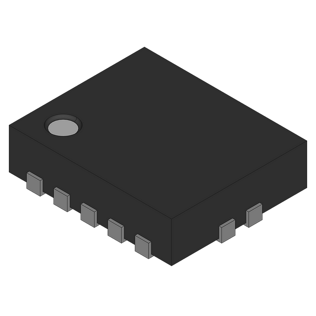
74AHCT04BQ,115 是 NXP USA Inc. 推出的六路反相器(Hex Inverter),属于 74AHCT 系列(Advanced High-Speed CMOS,TTL 兼容电平),采用 SOT763(DHVQFN14)无引线封装。其典型应用场景包括:

- 数字信号整形与电平转换:在混合逻辑系统中,将 TTL/5V CMOS 电平(输入兼容 3.3V–5.5V,输出驱动 5V)信号反相并增强驱动能力,常用于微控制器、FPGA 或 ASIC 的接口缓冲。

- 时钟与控制信号调理:对时钟、复位、使能等关键控制信号进行反相、去抖或波形整形,提升抗干扰性与边沿陡度(典型传播延迟约 7.5 ns @ VCC=5V)。

- 振荡电路构建:配合石英晶体或RC网络构成简单方波振荡器(如环形振荡器),用于低精度时钟源或测试信号发生。

- 总线驱动与隔离:在低功耗嵌入式系统中,用作单向信号反相隔离,避免负载反馈影响前级电路。

- 工业与消费电子接口:广泛应用于打印机、POS终端、工业HMI、LED驱动控制板及汽车信息娱乐系统(符合AEC-Q100 Grade 3,支持–40°C 至 +85°C 工业温度范围)。

该器件具有低功耗(静态电流 <1 µA)、高抗噪性(CMOS输入阈值)、无铅且符合RoHS,适用于空间受限、需稳定可靠逻辑反相的中低速数字系统。
| 参数 | 数值 |
| 产品目录 | 集成电路 (IC) |
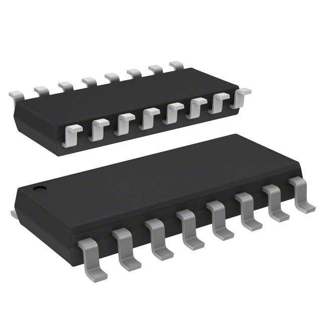
| 描述 | IC HEX INVERTER 14DHVQFN |
| 产品分类 | |
| 品牌 | NXP Semiconductors |
| 数据手册 | |
| 产品图片 |
|
| 产品型号 | 74AHCT04BQ,115 |
| PCN封装 | |
| PCN组件/产地 | |
| rohs | 无铅 / 符合限制有害物质指令(RoHS)规范要求 |
| 产品系列 | 74AHCT |
| 不同V、最大CL时的最大传播延迟 | 7.7ns @ 5V,50pF |
| 产品培训模块 | http://www.digikey.cn/PTM/IndividualPTM.page?site=cn&lang=zhs&ptm=24983 |
| 供应商器件封装 | 14-DHVQFN(2.5x3) |
| 其它名称 | 568-9099-1 |
| 包装 | 剪切带 (CT) |
| 安装类型 | 表面贴装 |
| 封装/外壳 | 14-VFQFN 裸露焊盘 |
| 工作温度 | -40°C ~ 125°C |
| 标准包装 | 1 |
| 特性 | - |
| 电压-电源 | 4.5 V ~ 5.5 V |
| 电流-输出高,低 | 8mA,8mA |
| 电流-静态(最大值) | 2µA |
| 电路数 | 6 |
| 输入数 | 6 |
| 逻辑电平-低 | 0.8V |
| 逻辑电平-高 | 2V |
| 逻辑类型 |


- 商务部:美国ITC正式对集成电路等产品启动337调查
- 曝三星4nm工艺存在良率问题 高通将骁龙8 Gen1或转产台积电
- 太阳诱电将投资9.5亿元在常州建新厂生产MLCC 预计2023年完工
- 英特尔发布欧洲新工厂建设计划 深化IDM 2.0 战略
- 台积电先进制程称霸业界 有大客户加持明年业绩稳了
- 达到5530亿美元!SIA预计今年全球半导体销售额将创下新高
- 英特尔拟将自动驾驶子公司Mobileye上市 估值或超500亿美元
- 三星加码芯片和SET,合并消费电子和移动部门,撤换高东真等 CEO
- 三星电子宣布重大人事变动 还合并消费电子和移动部门
- 海关总署:前11个月进口集成电路产品价值2.52万亿元 增长14.8%


PDF Datasheet 数据手册内容提取
74AHC04; 74AHCT04 hex inverter Rev. 6 — 7 November 2011 Product data sheet 1. General description The 74AHC04; 74AHCT04 is a high-speed Si-gate CMOS device and is pin compatible with Low-power Schottky TTL (LSTTL). It is specified in compliance with JEDEC standard No.7-A. The 74AHC04; 74AHCT04 provides six inverting buffers. 2. Features and benefits Balanced propagation delays Inputs accept voltages higher than V CC Input levels: For 74AHC04: CMOS level For 74AHCT04: TTL level ESD protection: HBM EIA/JESD22-A114F exceeds 2000V MM EIA/JESD22-A115-A exceeds 200V CDM EIA/JESD22-C101C exceeds 1000V Multiple package options Specified from 40C to +85C and from 40C to +125C 3. Ordering information Table 1. Ordering info rmation Type number Package Temperature range Name Description Version 74AHC04 74AHC04D 40C to +125C SO14 plastic small outline package; 14leads; SOT108-1 bodywidth 3.9mm 74AHC04PW 40C to +125C TSSOP14 plastic thin shrink small outline package; 14leads; SOT402-1 body width4.4mm 74AHC04BQ 40C to +125C DHVQFN14 plastic dual in-line compatible thermal enhanced SOT762-1 very thin quad flat package; no leads; 14terminals; body2.530.85mm
74AHC04; 74AHCT04 Nexperia hex inverter Table 1. Ordering information …continued Type number Package Temperature range Name Description Version 74AHCT04 74AHCT04D 40C to +125C SO14 plastic small outline package; 14leads; SOT108-1 bodywidth 3.9mm 74AHCT04PW 40C to +125C TSSOP14 plastic thin shrink small outline package; 14leads; SOT402-1 body width4.4mm 74AHCT04BQ 40C to +125C DHVQFN14 plastic dual in-line compatible thermal enhanced SOT762-1 very thin quad flat package; no leads; 14terminals; body2.530.85mm 4. Functional diagram 1 1 2 1 1A 1Y 2 1 3 4 3 2A 2Y 4 1 5 6 5 3A 3Y 6 1 9 8 9 4A 4Y 8 1 11 5A 5Y 10 11 10 13 6A 6Y 12 1 13 12 mna342 mna343 Fig 1. Logic symbol Fig 2. IEC logic symbol A Y mna341 Fig 3. Logic diagram (one inverter) 74AHC_AHCT04 All information provided in this document is subject to legal disclaimers. © Nexperia B.V. 2017. All rights reserved Product data sheet Rev. 6 — 7 November 2011 2 of 15
74AHC04; 74AHCT04 Nexperia hex inverter 5. Pinning information 5.1 Pinning C terminal 1 A C index area 1 V 1 14 1Y 2 13 6A 1A 1 14 VCC 2A 3 12 6Y 1Y 2 13 6A 2Y 4 04 11 5A 2A 3 12 6Y 3A 5 GND(1) 10 5Y 2Y 4 04 11 5A 3Y 6 9 4A 3A 5 10 5Y 7 8 3Y 6 9 4A D Y GND 7 8 4Y GN 4 001aac442 001aac441 Transparent top view (1) The die substrate is attached to the exposed die pad using conductive die attach material. It can not be used as a supply pin or input. Fig 4. Pin configuration SO14 and TSSOP14 Fig 5. Pin configuration DHVQFN14 5.2 Pin description Table 2. Pin descripti on Symbol Pin Description 1A, 2A, 3A, 4A, 5A, 6A 1, 3, 5, 9, 11, 13 data input 1Y, 2Y, 3Y, 4Y, 5Y, 6Y 2, 4, 6, 8, 10, 12 data output GND 7 ground (0V) V 14 supply voltage CC 6. Functional description Table 3. Function tab le[1] Input nA Output nY L H H L [1] H = HIGH voltage level; L = LOW voltage level. 74AHC_AHCT04 All information provided in this document is subject to legal disclaimers. © Nexperia B.V. 2017. All rights reserved Product data sheet Rev. 6 — 7 November 2011 3 of 15
74AHC04; 74AHCT04 Nexperia hex inverter 7. Limiting values Table 4. Limiting valu es In accordance with the Absolute Maximum Rating System (IEC 60134). Voltages are referenced to GND (ground = 0V). Symbol Parameter Conditions Min Max Unit V supply voltage 0.5 +7.0 V CC V input voltage 0.5 +7.0 V I I input clamping current V < 0.5V [1] 20 - mA IK I I output clamping current V <0.5V or V > V + 0.5V [1] 20 +20 mA OK O O CC I output current V =0.5V to (V + 0.5V) 25 +25 mA O O CC I supply current - +75 mA CC I ground current 75 - mA GND T storage temperature 65 +150 C stg P total power dissipation T =40Cto+125C [2] - 500 mW tot amb [1] The input and output voltage ratings may be exceeded if the input and output current ratings are observed. [2] For SO14 packages: above 70C the value of Ptot derates linearly at 8mW/K. For TSSOP14 packages: above 60C the value of Ptot derates linearly at 5.5mW/K. For DHVQFN14 packages: above 60C the value of Ptot derates linearly at 4.5mW/K. 8. Recommended operating conditions Table 5. Operating co nditions Symbol Parameter Conditions Min Typ Max Unit 74AHC04 V supply voltage 2.0 5.0 5.5 V CC V input voltage 0 - 5.5 V I V output voltage 0 - V V O CC T ambient temperature 40 +25 +125 C amb t/V input transition rise and fall rate V =3.0Vto3.6V - - 100 ns/V CC V =4.5Vto5.5V - - 20 ns/V CC 74AHCT04 V supply voltage 4.5 5.0 5.5 V CC V input voltage 0 - 5.5 V I V output voltage 0 - V V O CC T ambient temperature 40 +25 +125 C amb t/V input transition rise and fall rate V =4.5Vto5.5V - - 20 ns/V CC 74AHC_AHCT04 All information provided in this document is subject to legal disclaimers. © Nexperia B.V. 2017. All rights reserved Product data sheet Rev. 6 — 7 November 2011 4 of 15
74AHC04; 74AHCT04 Nexperia hex inverter 9. Static characteristics Table 6. Static charac teristics At recommended operating conditions; voltages are referenced to GND (ground = 0V). Symbol Parameter Conditions 25C 40Cto+85C 40Cto+125C Unit Min Typ Max Min Max Min Max 74AHC04 V HIGH-level V =2.0V 1.5 - - 1.5 - 1.5 - V IH CC input voltage V =3.0V 2.1 - - 2.1 - 2.1 - V CC V =5.5V 3.85 - - 3.85 - 3.85 - V CC V LOW-level V =2.0V - - 0.5 - 0.5 - 0.5 V IL CC input voltage V =3.0V - - 0.9 - 0.9 - 0.9 V CC V =5.5V - - 1.65 - 1.65 - 1.65 V CC V HIGH-level V =V orV OH I IH IL output voltage I =50A; V =2.0V 1.9 2.0 - 1.9 - 1.9 - V O CC I =50A; V =3.0V 2.9 3.0 - 2.9 - 2.9 - V O CC I =50A; V =4.5V 4.4 4.5 - 4.4 - 4.4 - V O CC I =4.0mA; V =3.0V 2.58 - - 2.48 - 2.40 - V O CC I =8.0mA; V =4.5V 3.94 - - 3.80 - 3.70 - V O CC V LOW-level V =V orV OL I IH IL output voltage I =50A; V =2.0V - 0 0.1 - 0.1 - 0.1 V O CC I =50A; V =3.0V - 0 0.1 - 0.1 - 0.1 V O CC I =50A; V =4.5V - 0 0.1 - 0.1 - 0.1 V O CC I =4.0mA; V =3.0V - - 0.36 - 0.44 - 0.55 V O CC I =8.0mA; V =4.5V - - 0.36 - 0.44 - 0.55 V O CC I input leakage V =5.5VorGND; - - 0.1 - 1.0 - 2.0 A I I current V =0Vto5.5V CC I supply current V =V orGND; I =0A; - - 2.0 - 20 - 40 A CC I CC O V =5.5V CC C input V =V orGND - 3 10 - 10 - 10 pF I I CC capacitance 74AHCT04 V HIGH-level V = 4.5Vto5.5V 2.0 - - 2.0 - 2.0 - V IH CC input voltage V LOW-level V = 4.5Vto5.5V - - 0.8 - 0.8 - 0.8 V IL CC input voltage V HIGH-level V =V orV ; V =4.5V OH I IH IL CC output voltage I =50A 4.4 4.5 - 4.4 - 4.4 - V O I =8.0mA 3.94 - - 3.80 - 3.70 - V O V LOW-level V =V orV ; V =4.5V OL I IH IL CC output voltage I =50A - 0 0.1 - 0.1 - 0.1 V O I =8.0mA - - 0.36 - 0.44 - 0.55 V O I input leakage V =5.5VorGND; - - 0.1 - 1.0 - 2.0 A I I current V =0Vto5.5V CC 74AHC_AHCT04 All information provided in this document is subject to legal disclaimers. © Nexperia B.V. 2017. All rights reserved Product data sheet Rev. 6 — 7 November 2011 5 of 15
74AHC04; 74AHCT04 Nexperia hex inverter Table 6. Static characteristics …continued At recommended operating conditions; voltages are referenced to GND (ground = 0V). Symbol Parameter Conditions 25C 40Cto+85C 40Cto+125C Unit Min Typ Max Min Max Min Max I supply current V =V orGND; I =0A; - - 2.0 - 20 - 40 A CC I CC O V =5.5V CC I additional per input pin; - - 1.35 - 1.5 - 1.5 mA CC supply current V =V 2.1V; other pins I CC at V orGND; I =0A; CC O V =4.5Vto5.5V CC C input V =V orGND - 3 10 - 10 - 10 pF I I CC capacitance 10. Dynamic characteristics Table 7. Dynamic cha racteristics Voltages are referenced to GND (ground = 0V); for test circuit see Figure7. Symbol Parameter Conditions 25C 40C to+85C 40C to+125C Unit Min Typ[1] Max Min Max Min Max 74AHC04 t propagation nAtonY; see Figure6 [2] pd delay V =3.0Vto3.6V CC C =15pF - 4.0 8.5 1.0 10.5 1.0 11.0 ns L C =50pF - 6.0 11.4 1.0 13 1.0 14.5 ns L V =4.5Vto5.5V CC C =15pF - 3.0 5.5 1.0 6.5 1.0 7.0 ns L C =50pF - 4.5 7.5 1.0 8.5 1.0 9.5 ns L C power f =1MHz; V =GNDtoV [3] - 13.5 - - - - - pF PD i I CC dissipation capacitance 74AHC_AHCT04 All information provided in this document is subject to legal disclaimers. © Nexperia B.V. 2017. All rights reserved Product data sheet Rev. 6 — 7 November 2011 6 of 15
74AHC04; 74AHCT04 Nexperia hex inverter Table 7. Dynamic characteristics …continued Voltages are referenced to GND (ground = 0V); for test circuit see Figure7. Symbol Parameter Conditions 25C 40C to+85C 40C to+125C Unit Min Typ[1] Max Min Max Min Max 74AHCT04; V =4.5Vto5.5V CC t propagation nAtonY; see Figure6 [2] pd delay C =15pF - 3.0 6.7 1.0 7.5 1.0 8.5 ns L C =50pF - 4.5 7.7 1.0 8.5 1.0 10.0 ns L C power f =1MHz; V =GNDtoV [3] - 13.9 - - - - - pF PD i I CC dissipation capacitance [1] Typical values are measured at nominal supply voltage (V =3.3V and V =5.0V). CC CC [2] t is the same as t and t . pd PLH PHL [3] CPD is used to determine the dynamic power dissipation (PD in W). PD=CPDVCC2fiN+(CLVCC2fo)where: f =input frequency in MHz; i f =output frequency in MHz; o C =output load capacitance inpF; L V =supply voltage in V; CC N=number of inputs switching; (CLVCC2fo)=sum of the outputs. 11. Waveforms VI nA input VM VM GND tPHL tPLH VOH nY output VM VM VOL mna344 Measurement points are given in Table8. V and V are typical output voltage drop that occur with the output load. OH OL Fig 6. Input to output propagation delay Table 8. Measuremen t points Type Input Output V V M M 74AHC04 0.5V 0.5V CC CC 74AHCT04 1.5 V 0.5V CC 74AHC_AHCT04 All information provided in this document is subject to legal disclaimers. © Nexperia B.V. 2017. All rights reserved Product data sheet Rev. 6 — 7 November 2011 7 of 15
74AHC04; 74AHCT04 Nexperia hex inverter VI tW 90 % negative pulse VM VM 10 % GND tf tr tr tf VI 90 % positive pulse VM VM 10 % GND tW VCC VI VO G DUT RT CL 001aah768 Test data is given in Table9. Definitions test circuit: RT = termination resistance should be equal to output impedance Zo of the pulse generator. C = load capacitance including jig and probe capacitance. L Fig 7. Load circuitry for measuring switching times Table 9. Test data Type Input Load Test V t, t C I r f L 74AHC04 V 3.0ns 15pF, 50pF t , t CC PLH PHL 74AHCT04 3.0V 3.0ns 15pF, 50pF t , t PLH PHL 74AHC_AHCT04 All information provided in this document is subject to legal disclaimers. © Nexperia B.V. 2017. All rights reserved Product data sheet Rev. 6 — 7 November 2011 8 of 15
74AHC04; 74AHCT04 Nexperia hex inverter 12. Package outline SO14: plastic small outline package; 14 leads; body width 3.9 mm SOT108-1 D E A X c y HE v M A Z 14 8 Q A2 A1 (A 3 ) A pin 1 index θ Lp 1 7 L e w M detail X bp 0 2.5 5 mm scale DIMENSIONS (inch dimensions are derived from the original mm dimensions) UNIT mAax. A1 A2 A3 bp c D(1) E(1) e HE L Lp Q v w y Z(1) θ 0.25 1.45 0.49 0.25 8.75 4.0 6.2 1.0 0.7 0.7 mm 1.75 0.25 1.27 1.05 0.25 0.25 0.1 0.10 1.25 0.36 0.19 8.55 3.8 5.8 0.4 0.6 0.3 8o 0.010 0.057 0.019 0.0100 0.35 0.16 0.244 0.039 0.028 0.028 0o inches 0.069 0.01 0.05 0.041 0.01 0.01 0.004 0.004 0.049 0.014 0.0075 0.34 0.15 0.228 0.016 0.024 0.012 Note 1. Plastic or metal protrusions of 0.15 mm (0.006 inch) maximum per side are not included. OUTLINE REFERENCES EUROPEAN ISSUE DATE VERSION IEC JEDEC JEITA PROJECTION 99-12-27 SOT108-1 076E06 MS-012 03-02-19 Fig 8. Package outline SOT108-1 (SO14) 74AHC_AHCT04 All information provided in this document is subject to legal disclaimers. © Nexperia B.V. 2017. All rights reserved Product data sheet Rev. 6 — 7 November 2011 9 of 15
74AHC04; 74AHCT04 Nexperia hex inverter TSSOP14: plastic thin shrink small outline package; 14 leads; body width 4.4 mm SOT402-1 D E A X c y HE v M A Z 14 8 Q A2 (A 3 ) A pin 1 index A1 θ Lp L 1 7 detail X w M e bp 0 2.5 5 mm scale DIMENSIONS (mm are the original dimensions) UNIT mAax. A1 A2 A3 bp c D(1) E(2) e HE L Lp Q v w y Z(1) θ mm 1.1 00..1055 00..9850 0.25 00..3109 00..21 54..19 44..53 0.65 66..62 1 00..7550 00..43 0.2 0.13 0.1 00..7328 80oo Notes 1. Plastic or metal protrusions of 0.15 mm maximum per side are not included. 2. Plastic interlead protrusions of 0.25 mm maximum per side are not included. OUTLINE REFERENCES EUROPEAN ISSUE DATE VERSION IEC JEDEC JEITA PROJECTION 99-12-27 SOT402-1 MO-153 03-02-18 Fig 9. Package outline SOT402-1 (TSSOP14) 74AHC_AHCT04 All information provided in this document is subject to legal disclaimers. © Nexperia B.V. 2017. All rights reserved Product data sheet Rev. 6 — 7 November 2011 10 of 15
74AHC04; 74AHCT04 Nexperia hex inverter DHVQFN14: plastic dual in-line compatible thermal enhanced very thin quad flat package; no leads; 14 terminals; body 2.5 x 3 x 0.85 mm SOT762-1 D B A A A1 E c terminal 1 detail X index area terminal 1 e1 C index area e b v M C A B y1 C y w M C 2 6 L 1 7 Eh e 14 8 13 9 Dh X 0 2.5 5 mm scale DIMENSIONS (mm are the original dimensions) A(1) UNIT max. A1 b c D(1) Dh E(1) Eh e e1 L v w y y1 0.05 0.30 3.1 1.65 2.6 1.15 0.5 mm 1 0.2 0.5 2 0.1 0.05 0.05 0.1 0.00 0.18 2.9 1.35 2.4 0.85 0.3 Note 1. Plastic or metal protrusions of 0.075 mm maximum per side are not included. OUTLINE REFERENCES EUROPEAN ISSUE DATE VERSION IEC JEDEC JEITA PROJECTION 02-10-17 SOT762-1 - - - MO-241 - - - 03-01-27 Fig 10. Package outline SOT762-1 (DHVQFN14) 74AHC_AHCT04 All information provided in this document is subject to legal disclaimers. © Nexperia B.V. 2017. All rights reserved Product data sheet Rev. 6 — 7 November 2011 11 of 15
74AHC04; 74AHCT04 Nexperia hex inverter 13. Abbreviations Table 10. Abbreviation s Acronym Description CDM Charged Device Model CMOS Complementary Metal-Oxide Semiconductor DUT Device Under Test ESD ElectroStatic Discharge HBM Human Body Model LSTTL Low-power Schottky Transistor-Transistor Logic MM Machine Model 14. Revision history T able 11. Revision history Document ID Release date Data sheet status Change notice Supersedes 74AHC_AHCT04 v.6 20111107 Product data sheet - 74AHC_AHCT04 v.5 Modifications: • Legal pages updated. 74AHC_AHCT04 v.5 20110411 Product data sheet - 74AHC_AHCT04 v.4 74AHC_AHCT04 v.4 20080514 Product data sheet - 74AHC_AHCT04 v.3 74AHC_AHCT04 v.3 20050207 Product data sheet - 74AHC_AHCT04 v.2 74AHC_AHCT04 v.2 19990927 Product specification - 74AHC_AHCT04 v.1 74AHC_AHCT04 v.1 19990225 Product specification - - 74AHC_AHCT04 All information provided in this document is subject to legal disclaimers. © Nexperia B.V. 2017. All rights reserved Product data sheet Rev. 6 — 7 November 2011 12 of 15
74AHC04; 74AHCT04 Nexperia hex inverter 15. Legal information 15.1 Data sheet status Document status[1][2] Product status[3] Definition Objective [short] data sheet Development This document contains data from the objective specification for product development. Preliminary [short] data sheet Qualification This document contains data from the preliminary specification. Product [short] data sheet Production This document contains the product specification. [1] Please consult the most recently issued document before initiating or completing a design. [2] The term ‘short data sheet’ is explained in section “Definitions”. [3] The product status of device(s) described in this document may have changed since this document was published and may differ in case of multiple devices. The latest product status information is available on the Internet at URLhttp://www.nexperia.com. 15.2 Definitions malfunction of a Nexperia product can reasonably be expected to result in personal injury, death or severe property or environmental damage. Nexperia accepts no liability for inclusion and/or use of Draft — The document is a draft version only. The content is still under Nexperia products in such equipment or applications and internal review and subject to formal approval, which may result in therefore such inclusion and/or use is at the customer’s own risk. modifications or additions. Nexperia does not give any representations or warranties as to the accuracy or completeness of Applications — Applications that are described herein for any of these information included herein and shall have no liability for the consequences of products are for illustrative purposes only. Nexperia makes no use of such information. representation or warranty that such applications will be suitable for the specified use without further testing or modification. Short data sheet — A short data sheet is an extract from a full data sheet with the same product type number(s) and title. A short data sheet is intended Customers are responsible for the design and operation of their applications for quick reference only and should not be relied upon to contain detailed and and products using Nexperia products, and Nexperia full information. For detailed and full information see the relevant full data accepts no liability for any assistance with applications or customer product sheet, which is available on request via the local Nexperia sales design. It is customer’s sole responsibility to determine whether the Nexperia office. In case of any inconsistency or conflict with the short data sheet, the product is suitable and fit for the customer’s applications and full data sheet shall prevail. products planned, as well as for the planned application and use of customer’s third party customer(s). Customers should provide appropriate Product specification — The information and data provided in a Product design and operating safeguards to minimize the risks associated with their data sheet shall define the specification of the product as agreed between applications and products. Nexperia and its customer, unless Nexperia and Nexperia does not accept any liability related to any default, customer have explicitly agreed otherwise in writing. In no event however, damage, costs or problem which is based on any weakness or default in the shall an agreement be valid in which the Nexperia product is customer’s applications or products, or the application or use by customer’s deemed to offer functions and qualities beyond those described in the third party customer(s). Customer is responsible for doing all necessary Product data sheet. testing for the customer’s applications and products using Nexperia products in order to avoid a default of the applications and 15.3 Disclaimers the products or of the application or use by customer’s third party customer(s). Nexperia does not accept any liability in this respect. Limited warranty and liability — Information in this document is believed to Limiting values — Stress above one or more limiting values (as defined in be accurate and reliable. However, Nexperia does not give any the Absolute Maximum Ratings System of IEC60134) will cause permanent representations or warranties, expressed or implied, as to the accuracy or damage to the device. Limiting values are stress ratings only and (proper) completeness of such information and shall have no liability for the operation of the device at these or any other conditions above those given in consequences of use of such information. the Recommended operating conditions section (if present) or the Characteristics sections of this document is not warranted. Constant or In no event shall Nexperia be liable for any indirect, incidental, repeated exposure to limiting values will permanently and irreversibly affect punitive, special or consequential damages (including - without limitation - lost the quality and reliability of the device. profits, lost savings, business interruption, costs related to the removal or replacement of any products or rework charges) whether or not such Terms and conditions of commercial sale — Nexperia damages are based on tort (including negligence), warranty, breach of products are sold subject to the general terms and conditions of commercial contract or any other legal theory. sale, as published at http://www.nexperia.com/profile/terms, unless otherwise Notwithstanding any damages that customer might incur for any reason agreed in a valid written individual agreement. In case an individual whatsoever, Nexperia’s aggregate and cumulative liability towards agreement is concluded only the terms and conditions of the respective customer for the products described herein shall be limited in accordance agreement shall apply. Nexperia hereby expressly objects to with the Terms and conditions of commercial sale of Nexperia. applying the customer’s general terms and conditions with regard to the purchase of Nexperia products by customer. Right to make changes — Nexperia reserves the right to make changes to information published in this document, including without No offer to sell or license — Nothing in this document may be interpreted or limitation specifications and product descriptions, at any time and without construed as an offer to sell products that is open for acceptance or the grant, notice. This document supersedes and replaces all information supplied prior conveyance or implication of any license under any copyrights, patents or to the publication hereof. other industrial or intellectual property rights. Suitability for use — Nexperia products are not designed, Export control — This document as well as the item(s) described herein authorized or warranted to be suitable for use in life support, life-critical or may be subject to export control regulations. Export might require a prior safety-critical systems or equipment, nor in applications where failure or authorization from competent authorities. 74AHC_AHCT04 All information provided in this document is subject to legal disclaimers. © Nexperia B.V. 2017. All rights reserved Product data sheet Rev. 6 — 7 November 2011 13 of 15
74AHC04; 74AHCT04 Nexperia hex inverter Non-automotive qualified products — Unless this data sheet expressly Nexperia’s specifications such use shall be solely at customer’s states that this specific Nexperia product is automotive qualified, own risk, and (c) customer fully indemnifies Nexperia for any the product is not suitable for automotive use. It is neither qualified nor tested liability, damages or failed product claims resulting from customer design and in accordance with automotive testing or application requirements. Nexperia use of the product for automotive applications beyond Nexperia’s accepts no liability for inclusion and/or use of standard warranty and Nexperia’s product specifications. non-automotive qualified products in automotive equipment or applications. In the event that customer uses the product for design-in and use in 15.4 Trademarks automotive applications to automotive specifications and standards, customer (a) shall use the product without Nexperia’s warranty of the Notice: All referenced brands, product names, service names and trademarks product for such automotive applications, use and specifications, and (b) are the property of their respective owners. whenever customer uses the product for automotive applications beyond 16. Contact information For more information, please visit: http://www.nexperia.com For sales office addresses, please send an email to: salesaddresses@nexperia.com 74AHC_AHCT04 All information provided in this document is subject to legal disclaimers. © Nexperia B.V. 2017. All rights reserved Product data sheet Rev. 6 — 7 November 2011 14 of 15
74AHC04; 74AHCT04 Nexperia hex inverter 17. Contents 1 General description. . . . . . . . . . . . . . . . . . . . . . 1 2 Features and benefits . . . . . . . . . . . . . . . . . . . . 1 3 Ordering information. . . . . . . . . . . . . . . . . . . . . 1 4 Functional diagram . . . . . . . . . . . . . . . . . . . . . . 2 5 Pinning information. . . . . . . . . . . . . . . . . . . . . . 3 5.1 Pinning . . . . . . . . . . . . . . . . . . . . . . . . . . . . . . . 3 5.2 Pin description . . . . . . . . . . . . . . . . . . . . . . . . . 3 6 Functional description . . . . . . . . . . . . . . . . . . . 3 7 Limiting values. . . . . . . . . . . . . . . . . . . . . . . . . . 4 8 Recommended operating conditions. . . . . . . . 4 9 Static characteristics. . . . . . . . . . . . . . . . . . . . . 5 10 Dynamic characteristics. . . . . . . . . . . . . . . . . . 6 11 Waveforms . . . . . . . . . . . . . . . . . . . . . . . . . . . . . 7 12 Package outline. . . . . . . . . . . . . . . . . . . . . . . . . 9 13 Abbreviations. . . . . . . . . . . . . . . . . . . . . . . . . . 12 14 Revision history. . . . . . . . . . . . . . . . . . . . . . . . 12 15 Legal information. . . . . . . . . . . . . . . . . . . . . . . 13 15.1 Data sheet status . . . . . . . . . . . . . . . . . . . . . . 13 15.2 Definitions. . . . . . . . . . . . . . . . . . . . . . . . . . . . 13 15.3 Disclaimers. . . . . . . . . . . . . . . . . . . . . . . . . . . 13 15.4 Trademarks. . . . . . . . . . . . . . . . . . . . . . . . . . . 14 16 Contact information. . . . . . . . . . . . . . . . . . . . . 14 17 Contents. . . . . . . . . . . . . . . . . . . . . . . . . . . . . . 15 © Nexperia B.V. 2017. All rights reserved For more information, please visit: http://www.nexperia.com For sales office addresses, please send an email to: salesaddresses@nexperia.com Date of release: 07 November 2011
Mouser Electronics Authorized Distributor Click to View Pricing, Inventory, Delivery & Lifecycle Information: N experia: 74AHC04BQ,115 74AHC04D,112 74AHC04D,118 74AHC04PW,112 74AHC04PW,118 74AHCT04BQ,115 74AHCT04D,112 74AHCT04D,118 74AHCT04PW,112 74AHCT04PW,118