ICGOO在线商城 > 分立半导体产品 > 晶闸管 - TRIAC > ACS108-6SN-TR

 Datasheet下载
- 型号: ACS108-6SN-TR
- 制造商: STMicroelectronics
- 库位|库存: xxxx|xxxx
- 要求:
| 数量阶梯 | 香港交货 | 国内含税 |
| +xxxx | $xxxx | ¥xxxx |
查看当月历史价格
查看今年历史价格
ACS108-6SN-TR产品简介:
ICGOO电子元器件商城为您提供ACS108-6SN-TR由STMicroelectronics设计生产,在icgoo商城现货销售,并且可以通过原厂、代理商等渠道进行代购。 ACS108-6SN-TR价格参考。STMicroelectronicsACS108-6SN-TR封装/规格:晶闸管 - TRIAC, TRIAC Logic - Sensitive Gate 600V 800mA Surface Mount SOT-223。您可以下载ACS108-6SN-TR参考资料、Datasheet数据手册功能说明书,资料中有ACS108-6SN-TR 详细功能的应用电路图电压和使用方法及教程。
STMicroelectronics的ACS108-6SN-TR是一款600V高灵敏度门极触发的TRIAC,属于晶闸管器件,适用于交流负载控制。该器件采用SOT-223封装,具有良好的热性能和紧凑尺寸,适合高密度PCB布局。

其主要应用场景包括:家用电器中的交流电机调速与开关控制,如洗衣机、风扇、吸尘器等;照明调光系统,特别是白炽灯或LED灯的相位调光电路;小型工业控制设备中的固态继电器替代方案;以及各类需要小功率交流负载控制的智能插座、温控器和电源开关模块。

ACS108-6SN-TR具备高抗噪能力和直接与微控制器输出兼容的门极灵敏度,可省去光耦驱动电路中的额外放大元件,简化设计并降低成本。同时,其符合国际安全标准(如IEC/EN 60730),适用于需要功能安全认证的消费类和工业类电器产品。

由于其最大负载电流为1A RMS,适合控制低至中等功率的交流负载(通常在几百瓦以内),广泛用于智能家居和自动化系统中的可靠、高效交流开关应用。
| 参数 | 数值 |
| 产品目录 | |
| 描述 | TRIAC SENS GATE 600V 0.8A SOT223双向可控硅 Transient Vltg Protected AC Switch |
| 产品分类 | 双向可控硅分离式半导体 |
| GateTriggerCurrent-Igt | 10 mA |
| GateTriggerVoltage-Vgt | 1 V |
| 品牌 | STMicroelectronics |
| 产品手册 | |
| 产品图片 |
|
| rohs | 符合RoHS无铅 / 符合限制有害物质指令(RoHS)规范要求 |
| 产品系列 | 晶体闸流管,双向可控硅,STMicroelectronics ACS108-6SN-TRACS™/A.S.D® |
| 数据手册 | |
| 产品型号 | ACS108-6SN-TR |
| 三端双向可控硅类型 | 逻辑 - 灵敏栅极 |
| 不重复通态电流 | 13.7 A |
| 产品培训模块 | http://www.digikey.cn/PTM/IndividualPTM.page?site=cn&lang=zhs&ptm=26297http://www.digikey.cn/PTM/IndividualPTM.page?site=cn&lang=zhs&ptm=26298 |
| 产品目录页面 | |
| 产品种类 | 双向可控硅 |
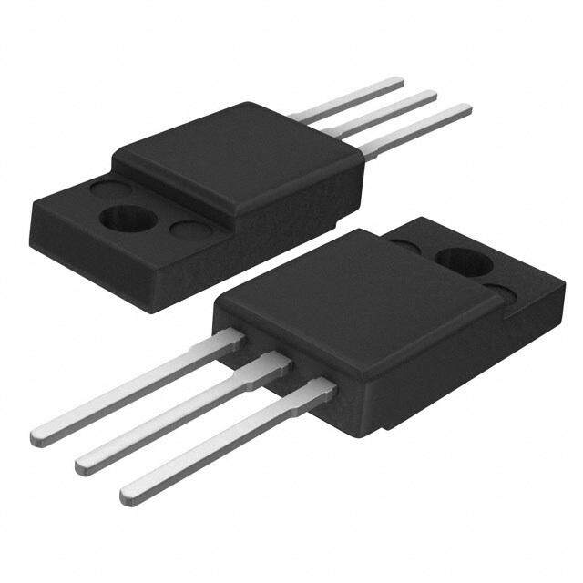
| 供应商器件封装 | SOT-223 |
| 保持电流Ih最大值 | 10 mA |
| 关闭状态漏泄电流(在VDRMIDRM下) | 2 uA |
| 其它名称 | 497-5568-2 |
| 其它有关文件 | http://www.st.com/web/catalog/sense_power/FM144/CL1208/SC477/PF62670?referrer=70071840 |
| 包装 | 带卷 (TR) |
| 商标 | STMicroelectronics |
| 安装类型 | 表面贴装 |
| 安装风格 | SMD/SMT |
| 封装 | Reel |
| 封装/外壳 | TO-261-4,TO-261AA |
| 封装/箱体 | SOT-223-4 |
| 工厂包装数量 | 1000 |
| 开启状态RMS电流-ItRMS | 0.8 A |
| 开启状态电压 | 1.3 V |
| 最大工作温度 | + 125 C |
| 最小工作温度 | - 30 C |
| 栅极触发电压-Vgt | 1 V |
| 栅极触发电流-Igt | 10 mA |
| 标准包装 | 1,000 |
| 电压-断态 | 600V |
| 电压-栅极触发(Vgt)(最大值) | 1V |
| 电流-不重复浪涌50、60Hz(Itsm) | 7.3A,7.6A |
| 电流-保持(Ih)(最大值) | 25mA |
| 电流-栅极触发(Igt)(最大值) | 10mA |
| 电流-通态(It(RMS))(最大值) | 800mA |
| 系列 | ACS108-6S |
| 配用 | /product-detail/zh/STEVAL-IHT004V1/497-9005-ND/2092933 |
| 配置 | 单一 |
| 额定重复关闭状态电压VDRM | 600 V |


- 商务部:美国ITC正式对集成电路等产品启动337调查
- 曝三星4nm工艺存在良率问题 高通将骁龙8 Gen1或转产台积电
- 太阳诱电将投资9.5亿元在常州建新厂生产MLCC 预计2023年完工
- 英特尔发布欧洲新工厂建设计划 深化IDM 2.0 战略
- 台积电先进制程称霸业界 有大客户加持明年业绩稳了
- 达到5530亿美元!SIA预计今年全球半导体销售额将创下新高
- 英特尔拟将自动驾驶子公司Mobileye上市 估值或超500亿美元
- 三星加码芯片和SET,合并消费电子和移动部门,撤换高东真等 CEO
- 三星电子宣布重大人事变动 还合并消费电子和移动部门
- 海关总署:前11个月进口集成电路产品价值2.52万亿元 增长14.8%


PDF Datasheet 数据手册内容提取
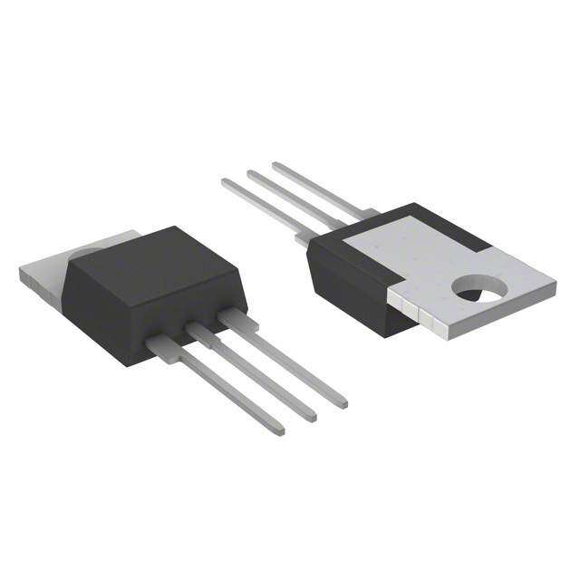
ACS108 Overvoltage protected AC switch (ACS™) Datasheet - production data Description COM The ACS108 belongs to the AC switch range (built with A. S. D.® technology). This high performance switch can control a load of up to 0.8 COM G COM A. The ACS108 switch includes an overvoltage OUT G OUT crowbar structure to absorb the inductive turn-off TO-92 SOT-223 energy, and a gate level shifter driver to separate ACS108-6SA ACS108-6SN the digital controller from the main switch. It is ACS108-8SA ACS108-8SN triggered with a negative gate current flowing out of the gate pin. Features Figure 1. Functional diagram OUT Enables equipment to meet IEC 61000-4-5 surge with overvoltage crowbar technology High noise immunity against static dV/dt and G IEC 61000-4-4 burst Needs no external protection snubber or varistor COM Reduces component count by up to 80% and COM Common drive reference to connect Interfaces directly with the micro-controller to the mains OUT Output to connect to the load. G Gate input to connect to the controller Common package tab connection supports through gate resistor connection of several alternating current switches on the same cooling pad Table 1. Device summary V gives headroom before clamping then CL crowbar action Symbol Value Unit I 0.8 A T(RMS) Applications V , V 600 and 800 V DRM RRM Alternating current on/off static switching in IGT 10 mA appliances and industrial control systems Driving low power high inductive or resistive loads like: – relay, valve, solenoid, dispenser, – pump, fan, low power motor, door lock – lamp ®: A.S.D. is a registered trademark of STMicroelectronics TM: ACS is a trademark of STMicroelectronics October 2013 DocID6518 Rev 5 1/13 This is information on a product in full production. www.st.com
Characteristics ACS108 1 Characteristics Tab le 2. Absolute maximum ratings (T = 25 °C, unless otherwise specified) amb Symbol Parameter Value Unit T = 64 °C 0.45 A amb TO-92 T = 76 °C lead I On-state rms current (full sine wave) T(RMS) SOT-223 Tamb = 76 °C 0.8 A S = 5 cm2 T = 104 °C tab Non repetitive surge peak on-state current F = 60 Hz t = 16.7 ms 13.7 I A TSM (full cycle sine wave, Tj initial = 25 °C) F = 50 Hz t = 20 ms 13 I2t I²t Value for fusing t = 10 ms 1.1 A2s p Critical rate of rise of on-state current dI/dt F = 120 Hz T = 125 °C 100 A/µs I = 2xI , t 100 ns j G GT r V Non repetitive mains peak mains voltage(1) 2 kV PP I Peak gate current t = 20 µs T = 125 °C 1 A GM p j V Peak positive gate voltage T = 125 °C 10 V GM j P Average gate power dissipation T = 125 °C 0.1 W G(AV) j T Storage junction temperature range -40 to +150 stg °C T Operating junction temperature range -30 to +125 j 1. According to test described by IEC 61000-4-5 standard and Figure18 T able 3. Electrical characteristics (T = 25 °C, unless otherwise specified) j Symbol Test conditions Quadrant Value Unit I (1) II - III Max. 10 mA GT V = 12 V, R = 33 OUT L V II - III Max. 1 V GT V V = V , R = 3.3 kT = 125 °C II - III Min. 0.15 V GD OUT DRM L j I I = 100 mA Max. 10 mA H OUT I I = 1.2 x I Max. 25 mA L G GT V = 402 V, gate open, T = 125 °C Min. 2000 V/µs OUT j dV/dt V = 536 V, gate open, T = 125 °C Min. 400 V/µs OUT j (dI/dt)c Without snubber (15 V/µs), T = 125 °C, turn-off time 20 ms Min. 2 A/ms j I = 0.1 mA, t = 1 ms, ACS108-6 Min. 650 V CL p V CL I = 0.1 mA, t = 1 ms, ACS108-8 Min. 850 V CL p 1. Minimum I is guaranteed at 10% of I max GT GT 2/13 DocID6518 Rev 5
ACS108 Characteristics Table 4. Static electrical characteristics Symbol Parameter and test conditions Value Unit V (1) I = 1.1 A, t = 500 µs T = 25 °C Max. 1.3 V TM TM p j V (1) Threshold voltage T = 125 °C Max. 0.85 V t0 j R (1) Dynamic resistance T = 125 °C Max. 300 m D j IDRM V = V = V Tj = 25 °C Max. 2 µA IRRM OUT DRM RRM Tj = 125 °C 0.2 mA 1. For both polarities of OUT referenced to COM Table 5. Thermal resistance Symbol Parameter Value Unit R Junction to lead (AC) TO-92 Max. 60 th (j-l) R Junction to tab (AC) SOT-223 Max. 25 th (j-t) °C/W TO-92 Max. 150 R Junction to ambient th (j-a) S = 5 cm² SOT-223 Max. 60 Figure 2. Maximum power dissipation versus Figure 3. On-state rms current versus case on-state rms current temperature (SOT223) P (W) IT(RMS)(A) 0.9 0.9 α= 180° 0.8 0.8 (cid:2)=180° 0.7 0.7 SOT-223 0.6 0.6 0.5 0.5 0.4 0.4 0.3 0.3 0.2 180° 0.2 0.1 IT(RMS)(A) 0.1 TC°C 0.0 0.0 0.0 0.1 0.2 0.3 0.4 0.5 0.6 0.7 0.8 0 25 50 75 100 125 DocID6518 Rev 5 3/13 13
Characteristics ACS108 Figure 4. On-state rms current versus ambient Figure 5. Relative variation of thermal temperature (free air convection) impedance junction to ambient versus pulse duration 0.9IT(RMS)(A) 1.00 K=[Zth(j-a)/Rth(j-a)] (cid:2)=180° Zth(j-a) 0.8 SOT-223 0.7 TO-92 0.6 0.5 0.10 0.4 TO-92 0.3 SOT-223 0.2 Single layer Printed SOT-223 0.1 Ncairtcuuriat lb cooanrvde FcRtio4n Ta°C tP(s) Coaprepae r= s 5ucrfmac²e 0.0 0.01 0 25 50 75 100 125 1.0E-03 1.0E-02 1.0E-01 1.0E+00 1.0E+01 1.0E+02 1.0E+03 Figure 6. Relative variation of holding and Figure 7. Relative variation of I and V GT GT latching current versus junction temperature versus junction temperature 3.0 IH,IL[Tj]/IH,IL[Tj=25°C] 3.5 IGT,VGT[Tj]/IGT,VGT, [Tj=25°C] 2.5 3.0 IGTQ2 IL 2.5 IGTQ3 2.0 2.0 1.5 IH 1.5 1.0 1.0 VGTQ2-Q3 0.5 0.5 Tj(°C) Tj(°C) 0.0 0.0 -50 -25 0 25 50 75 100 125 -50 -25 0 25 50 75 100 125 Figure 8. Surge peak on-state current versus Figure 9. Non repetitive surge peak on-state number of cycles current for a sinusoidal pulse, and corresponding value of I²t 14 ITSM(A) ITSM(A),I²t(A²s) 1.E+03 13 Sinusoidal pulse, 12 tp< 10 ms 1101 t=O20nme scycle 1.E+02 ITSM Tjinitial = 25 °C Non repetitive 9 Tjinitial=25°C 8 7 SOT-223 1.E+01 Repetitive 6 Ttab = 104°C 5 4 1.E+00 3 I²t TO-92 2 Repetitive 1 Tlead= 76°C Number of cycles tp(ms) 0 1.E-01 1 10 100 1000 0.01 0.10 1.00 10.00 4/13 DocID6518 Rev 5
ACS108 Characteristics Figure 10. On-state characteristics (maximum Figure 11. Relative variation of critical rate of values) decrease of main current versus junction temperature I (A) 100.00 TM (dI/dt)c[Tj] / (dI/dt)c[Tj=125 °C] 2.5 2.0 10.00 1.5 1.0 1.00 Tj=125°C Tj=25°C Tjmax.: 0.5 0.10 VTM(V) RVdt=o= 3 00.08 5m VΩ 0.0 Tj(°C) 25 35 45 55 65 75 85 95 105 115 125 0.0 0.5 1.0 1.5 2.0 2.5 3.0 3.5 4.0 4.5 Figure 12. Relative variation of static dV/dt Figure 13. Relative variation of leakage current immunity versus junction temperature(1) versus junction temperature 5 dV/dt[Tj]/dV/dt[Tj=125°C] 1.0E+00 IDRM/IRRM[Tj;VDRM/VRRM]/IDRM/IRRM[Tj=125°C;800V] VD=VR=536V 4 1.0E-01 VDRM=VRRM=800 V 3 VDRM=VRRM=600 V 2 1.0E-02 1 Tj(°C) Tj(°C) 0 1.0E-03 25 50 75 100 125 25 50 75 100 125 1. V = V = 402 V: Typical values above 5 kV/µs. Beyond equipment capability D R Figure 14. Relative variation of critical rate of Figure 15. Thermal resistance junction to decrease of main current (di/dt)c versus ambient versus copper surface under tab (dV/dt)c (SOT-223) 5.0 (dI/dt)c[(dV/dt)c]/Specified(dI/dt)c 140 Rth(j-a)(°C/W) 4.5 Tj =125°C Pcoripnpteedr tchiricckunite bsosa =rd 3 F5 Rµ4m SOT-223 120 4.0 3.5 100 3.0 80 2.5 60 2.0 1.5 40 1.0 20 0.5 (dV/dt)c(V/µs) SCU(cm²) 0.0 0 0.1 1.0 10.0 100.0 0.0 0.5 1.0 1.5 2.0 2.5 3.0 3.5 4.0 4.5 5.0 DocID6518 Rev 5 5/13 13
Alternating current mains switch - basic application ACS108 2 Alternating current mains switch - basic application The ACS108 switch is triggered by a negative gate current flowing from the gate pin G. The switch can be driven directly by the digital controller through a resistor as shown in Figure16. Thanks to its overvoltage protection and turn-off commutation performance, the ACS108 switch can drive a small power high inductive load with neither varistor nor additional turn-off snubber. Figure 16. Typical application schematic Valve AC Mains ACS108 Vss Rg V MCU T Power supply Vdd 220Ω I T 2.1 Protection against overvoltage: the best choice is ACS In comparison with standard Triacs the ACS108 is over-voltage self-protected, as specified by the new parameter V . This feature is useful in two operating conditions: in case of turn- CL off of very inductive load, and in case of surge voltage that can occur on the electrical network. 2.1.1 High inductive load switch-off: turn-off overvoltage clamping With high inductive and low rms current loads the rate of decrease of the current is very low. An overvoltage can occur when the gate current is removed and the OUT current is lower than I . H As shown in Figure17, at the end of the last conduction half-cycle, the load current decreases ①. The load current reaches the holding current level I ②, and the ACS turns H off ③. The water valve, as an inductive load (up to 15 H), reacts as a current generator and an overvoltage is created, which is clamped by the ACS ④. The current flows through the ACS avalanche and decreases linearly to zero. During this time, the voltage across the switch is limited to the clamping voltage V . The energy stored in the inductance of the CL load is dissipated in the clamping section that is designed for this purpose. When the energy has been dissipated, the ACS voltage falls back to the mains voltage value (230 V rms, 50Hz)⑤. 6/13 DocID6518 Rev 5
ACS108 Alternating current mains switch - basic application Figure 17. Switching off of a high inductive load - typical clamping capability of ACS108 (T = 25 °C) amb 4 V CL IIT 11 3 V T 22 33 (200V/div) IIHH 44 IT 55 VVT (5 mA/div) VVCCLL 1 I H 2 5 100 µs/div 2.1.2 Alternating current mains transient voltage ruggedness The ACS108 switch is able to withstand safely the AC mains transients either by clamping the low energy spikes or by breaking-over when subjected to high energy shocks, even with high turn-on current rises. The test circuit shown in Figure18 is representative of the final ACS108 application, and is also used to test the AC switch according to the IEC 61000-4-5 standard conditions. Thanks to the load limiting the current, the ACS108 switch withstands the voltage spikes up to 2 kV above the peak mains voltage. The protection is based on an overvoltage crowbar technology. Actually, the ACS108 breaks over safely as shown in Figure19. The ACS108 recovers its blocking voltage capability after the surge (switch off back at the next zero crossing of the current). Such non-repetitive tests can be done 10 times on each AC mains voltage polarity. Figure 18. Overvoltage ruggedness test circuit for resistive and inductive loads, T amb = 25 °C (conditions equivalent to IEC61000-4-5 standard) +2 kV surge generator Load CC 150Ω 5 µH ACS108 OUT Mains V T G voltage 230V rms COM 50 Hz 220Ω IT DocID6518 Rev 5 7/13 13
Alternating current mains switch - basic application ACS108 Figure 19. Typical current and voltage waveforms across the ACS108 (+2 kV surge, IEC 61000-4-5 standard) V (200V/div) T I = 17.2 A T max dI /dt= 1.8 A/µs T I (4 A/div) T 500 ns/div 8/13 DocID6518 Rev 5
ACS108 Package information 3 Package information Epoxy meets UL94, V0 Lead-free packages In order to meet environmental requirements, ST offers these devices in different grades of ECOPACK® packages, depending on their level of environmental compliance. ECOPACK® specifications, grade definitions and product status are available at: www.st.com. ECOPACK® is an ST trademark. Figure 20. TO-92 dimension definitions A a B C F D E Table 6. TO-92 dimension values Dimensions Ref Millimeters Inches Min. Typ. Max. Min. Typ. Max. A 1.35 0.053 B 4.70 0.185 C 2.54 0.100 D 4.40 0.173 E 12.70 0.500 F 3.70 0.146 a 0.50 0.019 DocID6518 Rev 5 9/13 13
Package information ACS108 Figure 21. SOT-223 dimension definitions A V c A1 B e1 D B1 4 H E 1 2 3 e Table 7. SOT-223 dimension values Dimensions Ref. Millimeters Inches Min. Typ. Max. Min. Typ. Max. A 1.80 0.071 A1 0.02 0.10 0.001 0.004 B 0.60 0.70 0.85 0.024 0.027 0.033 B1 2.90 3.00 3.15 0.114 0.118 0.124 c 0.24 0.26 0.35 0.009 0.010 0.014 D(1) 6.30 6.50 6.70 0.248 0.256 0.264 e 2.3 0.090 e1 4.6 0.181 E(1) 3.30 3.50 3.70 0.130 0.138 0.146 H 6.70 7.00 7.30 0.264 0.276 0.287 V 10° max 1. Do not include mold flash or protrusions. Mold flash or protrusions shall not exceed 0.15mm (0.006inches) Figure 22. SOT-223 footprint (dimensions in mm) 3.25 1.32 5.16 7.80 1.32 2.30 0.95 10/13 DocID6518 Rev 5
ACS108 Ordering information 4 Ordering information Figure 23. Ordering information scheme ACS 1 08 - 6 S A -TR AC switch series Number of switches Current 08 = 0.8 A rms Voltage 6 = 600V 8 = 800V Sensitivity S = 10 mA Package A =TO-92 N = SOT-223 Packing TR =Tape and reel 7”(SOT-223, 1000 pieces) 13”(TO-92, 2000 pieces) AP = Ammopack (TO-92, 2000 pieces) Blank =bulk(TO-92, 2500 pieces) Table 8. Ordering information Order code Marking Package Weight Base Qty Delivery mode ACS108-6SA TO-92 0.2 g 2500 Bulk ACS108-6SA-TR ACS1 086SA TO-92 0.2 g 2000 Tape and reel ACS108-6SA-AP TO-92 0.2 g 2000 Ammopack ACS108-6SN-TR ACS 108 6SN SOT-223 0.11 g 1000 Tape and reel ACS108-8SA TO-92 0.2 g 2500 Bulk ACS108-8SA-TR ACS1 088SA TO-92 0.2 g 2000 Tape and reel ACS108-8SA-AP TO-92 0.2 g 2000 Ammopack ACS108-8SN-TR ACS 108 8SN SOT-223 0.11 g 1000 Tape and reel DocID6518 Rev 5 11/13 13
Revision history ACS108 5 Revision history Table 9. Document revision history Date Revision Changes Initial release. This datasheet covers order codes previously Apr_2004 1 described in the datasheet for ACS108-6S, Doc ID 11962, Rev 3 December 2010. 21-Jun-2005 2 Marking information updated from ACSxxxx to ACS1xxx. 11-Jul-2012 3 Removed 500 V devices and added 600 V and 800 V devices. 27-Sep-2013 4 Corrected typographical error in Figure4. 31-Oct-2013 5 Corrected character formatting issues in Section2.1.1. 12/13 DocID6518 Rev 5
ACS108 Please Read Carefully: Information in this document is provided solely in connection with ST products. STMicroelectronics NV and its subsidiaries (“ST”) reserve the right to make changes, corrections, modifications or improvements, to this document, and the products and services described herein at any time, without notice. All ST products are sold pursuant to ST’s terms and conditions of sale. Purchasers are solely responsible for the choice, selection and use of the ST products and services described herein, and ST assumes no liability whatsoever relating to the choice, selection or use of the ST products and services described herein. No license, express or implied, by estoppel or otherwise, to any intellectual property rights is granted under this document. If any part of this document refers to any third party products or services it shall not be deemed a license grant by ST for the use of such third party products or services, or any intellectual property contained therein or considered as a warranty covering the use in any manner whatsoever of such third party products or services or any intellectual property contained therein. UNLESS OTHERWISE SET FORTH IN ST’S TERMS AND CONDITIONS OF SALE ST DISCLAIMS ANY EXPRESS OR IMPLIED WARRANTY WITH RESPECT TO THE USE AND/OR SALE OF ST PRODUCTS INCLUDING WITHOUT LIMITATION IMPLIED WARRANTIES OF MERCHANTABILITY, FITNESS FOR A PARTICULAR PURPOSE (AND THEIR EQUIVALENTS UNDER THE LAWS OF ANY JURISDICTION), OR INFRINGEMENT OF ANY PATENT, COPYRIGHT OR OTHER INTELLECTUAL PROPERTY RIGHT. ST PRODUCTS ARE NOT DESIGNED OR AUTHORIZED FOR USE IN: (A) SAFETY CRITICAL APPLICATIONS SUCH AS LIFE SUPPORTING, ACTIVE IMPLANTED DEVICES OR SYSTEMS WITH PRODUCT FUNCTIONAL SAFETY REQUIREMENTS; (B) AERONAUTIC APPLICATIONS; (C) AUTOMOTIVE APPLICATIONS OR ENVIRONMENTS, AND/OR (D) AEROSPACE APPLICATIONS OR ENVIRONMENTS. WHERE ST PRODUCTS ARE NOT DESIGNED FOR SUCH USE, THE PURCHASER SHALL USE PRODUCTS AT PURCHASER’S SOLE RISK, EVEN IF ST HAS BEEN INFORMED IN WRITING OF SUCH USAGE, UNLESS A PRODUCT IS EXPRESSLY DESIGNATED BY ST AS BEING INTENDED FOR “AUTOMOTIVE, AUTOMOTIVE SAFETY OR MEDICAL” INDUSTRY DOMAINS ACCORDING TO ST PRODUCT DESIGN SPECIFICATIONS. PRODUCTS FORMALLY ESCC, QML OR JAN QUALIFIED ARE DEEMED SUITABLE FOR USE IN AEROSPACE BY THE CORRESPONDING GOVERNMENTAL AGENCY. Resale of ST products with provisions different from the statements and/or technical features set forth in this document shall immediately void any warranty granted by ST for the ST product or service described herein and shall not create or extend in any manner whatsoever, any liability of ST. ST and the ST logo are trademarks or registered trademarks of ST in various countries. Information in this document supersedes and replaces all information previously supplied. The ST logo is a registered trademark of STMicroelectronics. All other names are the property of their respective owners. © 2013 STMicroelectronics - All rights reserved STMicroelectronics group of companies Australia - Belgium - Brazil - Canada - China - Czech Republic - Finland - France - Germany - Hong Kong - India - Israel - Italy - Japan - Malaysia - Malta - Morocco - Philippines - Singapore - Spain - Sweden - Switzerland - United Kingdom - United States of America www.st.com DocID6518 Rev 5 13/13 13
Mouser Electronics Authorized Distributor Click to View Pricing, Inventory, Delivery & Lifecycle Information: S TMicroelectronics: ACS108-6SA ACS108-6SA-AP ACS108-6SA-TR ACS108-6SN-TR ACS108-8SA-TR ACS108-8SN-TR ACS108- 8SA ACS108-8SA-AP