 Datasheet下载
- 型号: 71V124SA10PHG
- 制造商: Integrated Device Technology
- 库位|库存: xxxx|xxxx
- 要求:
| 数量阶梯 | 香港交货 | 国内含税 |
| +xxxx | $xxxx | ¥xxxx |
查看当月历史价格
查看今年历史价格
71V124SA10PHG产品简介:
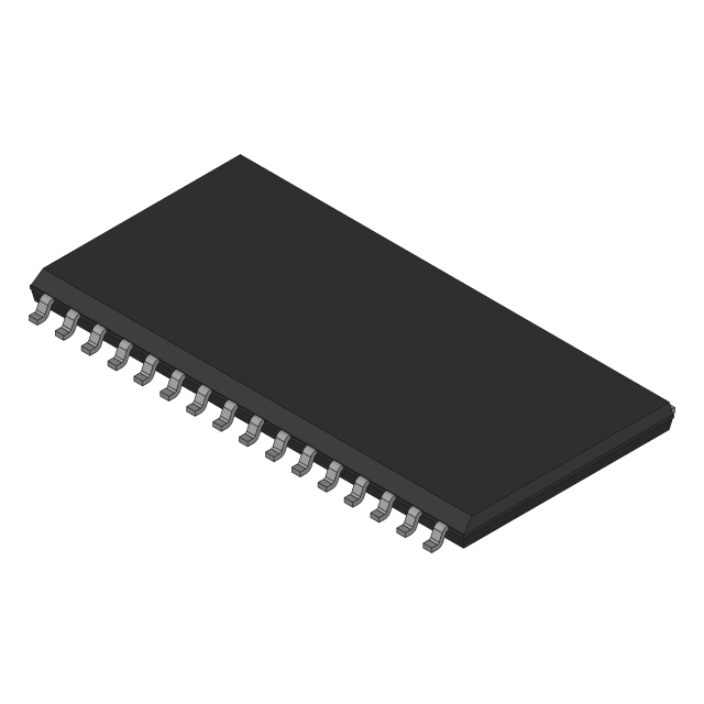
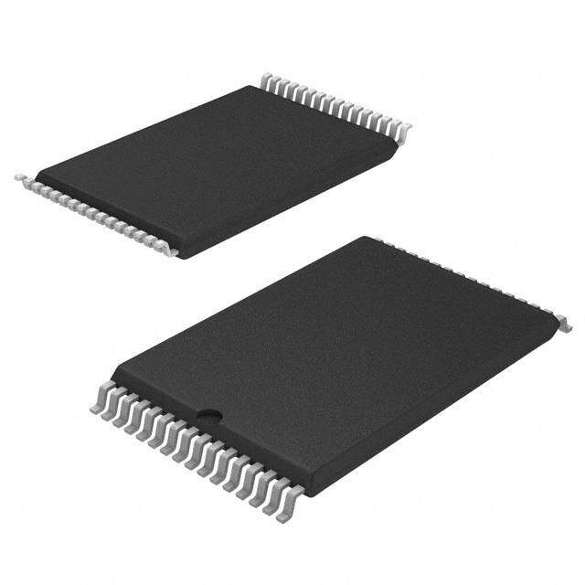
ICGOO电子元器件商城为您提供71V124SA10PHG由Integrated Device Technology设计生产,在icgoo商城现货销售,并且可以通过原厂、代理商等渠道进行代购。 71V124SA10PHG价格参考¥20.29-¥20.29。Integrated Device Technology71V124SA10PHG封装/规格:存储器, SRAM - 异步 存储器 IC 1Mb (128K x 8) 并联 10ns 32-TSOP II。您可以下载71V124SA10PHG参考资料、Datasheet数据手册功能说明书,资料中有71V124SA10PHG 详细功能的应用电路图电压和使用方法及教程。
IDT(Integrated Device Technology Inc.)生产的71V124SA10PHG是一款高速CMOS静态随机存取存储器(SRAM),属于异步SRAM产品系列。该型号为16位宽、容量为512K × 16(即总容量约8Mb)的低功耗高性能SRAM,采用先进的制造工艺,工作电压通常为3.3V,具备快速访问时间(典型为10纳秒),适用于对数据读写速度要求较高的场合。

71V124SA10PHG广泛应用于需要高速缓存和实时数据处理的电子系统中。典型应用场景包括通信设备(如路由器、交换机、基站中的缓冲存储)、工业控制设备(如PLC、数控系统)、网络基础设施设备、测试与测量仪器以及嵌入式系统等。由于其高可靠性和稳定性,也常用于航空航天、医疗设备等对元器件性能要求严苛的领域。

该器件采用标准的44引脚TSOP II或SOP封装(具体以数据手册为准),兼容行业通用接口设计,便于在多种电路板上集成。此外,其低功耗特性使其在注重能效的系统中具有优势。

综上所述,71V124SA10PHG凭借其高速、稳定和可靠的性能,主要应用于高端工业、通信及嵌入式系统中,作为临时数据存储或高速缓存使用,是许多实时处理系统中不可或缺的关键存储元件。
| 参数 | 数值 |
| 品牌 | IDT |
| 产品目录 | 半导体 |
| 描述 | 静态随机存取存储器 128Kx8 ASYNCHRONOUS 3.3V STATIC RAM |
| 产品分类 | 集成电路 - IC |
| 产品手册 | http://www.idt.com/document/dst/71v124sa-datasheet |
| 产品图片 |
|
| rohs | 符合RoHS |
| 产品系列 | 内存,静态随机存取存储器,IDT 71V124SA10PHG |
| 产品型号 | 71V124SA10PHG |
| 产品种类 | 静态随机存取存储器 |
| 商标 | IDT |
| 存储容量 | 1 Mbit |
| 存储类型 | SDR |
| 安装风格 | SMD/SMT |
| 封装 | Tube |
| 封装/箱体 | TSOP-32 |
| 工厂包装数量 | 23 |
| 接口 | Parallel |
| 最大工作温度 | + 70 C |
| 最大工作电流 | 145 mA |
| 最小工作温度 | 0 C |
| 电源电压-最大 | 3.6 V |
| 电源电压-最小 | 3.15 V |
| 类型 | Asynchronous |
| 系列 | 71V124 |
| 组织 | 128 k x 8 |
| 访问时间 | 10 ns |
| 零件号别名 | 71V124 IDT71V124SA10PHG |


- 商务部:美国ITC正式对集成电路等产品启动337调查
- 曝三星4nm工艺存在良率问题 高通将骁龙8 Gen1或转产台积电
- 太阳诱电将投资9.5亿元在常州建新厂生产MLCC 预计2023年完工
- 英特尔发布欧洲新工厂建设计划 深化IDM 2.0 战略
- 台积电先进制程称霸业界 有大客户加持明年业绩稳了
- 达到5530亿美元!SIA预计今年全球半导体销售额将创下新高
- 英特尔拟将自动驾驶子公司Mobileye上市 估值或超500亿美元
- 三星加码芯片和SET,合并消费电子和移动部门,撤换高东真等 CEO
- 三星电子宣布重大人事变动 还合并消费电子和移动部门
- 海关总署:前11个月进口集成电路产品价值2.52万亿元 增长14.8%


PDF Datasheet 数据手册内容提取
3.3V CMOS Static RAM 71V124SA 1 Meg (128K x 8-Bit) Center Power & Ground Pinout Features Description ◆◆◆◆◆ 128K x 8 advanced high-speed CMOS static RAM The IDT71V124 is a 1,048,576-bit high-speed static RAM organized ◆◆◆◆◆ JEDEC revolutionary pinout (center power/GND) for as 128K x 8. It is fabricated using high-performance, high-reliability CMOS reduced noise technology. This state-of-the-art technology, combined with innovative ◆◆◆◆◆ Equal access and cycle times circuit design techniques, provides a cost-effective solution for high-speed – Commercial: 10/12/15ns memory needs. The JEDEC center power/GND pinout reduces noise – Industrial: 10/12/15ns generation and improves system performance. ◆◆◆◆◆ One Chip Select plus one Output Enable pin The IDT71V124 has an output enable pin which operates as fast as ◆◆◆◆◆ Inputs and outputs are LVTTL-compatible 5ns, with address access times as fast as 10ns available. All bidirectional ◆◆◆◆◆ Single 3.3V supply inputs and outputs of the IDT71V124 are LVTTL-compatible and operation ◆◆◆◆◆ Low power consumption via chip deselect is from a single 3.3V supply. Fully static asynchronous circuitry is used; ◆◆◆◆◆ Available in a 32-pin 300- and 400-mil Plastic SOJ, and no clocks or refreshes are required for operation. 32-pin Type II TSOP packages ◆◆◆◆◆ Industrial temperature range (–40°C to +85°C) is available for selected speeds ◆◆◆◆◆ Green parts available, see ordering information Functional Block Diagram A0 • (cid:129) (cid:129) (cid:129) 1,048,576-BIT ADDRESS MEMORYARRAY (cid:129) (cid:129) DECODER A16 8 8 I/O0-I/O7 I/OCONTROL . 8 WE CONTROL OE LOGIC CS 3873drw01 1 Jun.30.20
71V124SA, 3.3V CMOS Static RAM 1 Meg (128K x 8-Bit) Center Power & Ground Pinout Commercial and Industrial Temperature Ranges Pin Configurations(1) Absolute Maximum Ratings(1) Symbol Rating Value Unit A0 1 32 A16 VDD Supply Voltage Relative -0.5 to +4.6 V A1 2 31 A15 to GND A2 3 30 A14 A3 4 29 A13 VIN, VOUT Terminal Voltage Relative -0.5 to VDD+0.5 V to GND CS 5 71V124 28 OE I/O0 6 PJG32 27 I/O7 Commercial I/O1 7 PBG32 26 I/O6 Operating Temperature -0 to +70 VDD 8 PHG32 25 GND TA oC GND 9 24 VDD Industrial I/O2 10 23 I/O5 Operating Temperature -40 to +85 I/O3 11 22 I/O4 WE 12 21 A12 TBIAS Temperature Under Bias -55 to +125 oC A4 13 20 A11 A5 14 19 A10 TSTG Storage Temperature -55 to +125 oC A6 15 18 A9 A7 16 17 A8 PT Power Dissipation 1.25 W 3873 drw 02 IOUT DC Output Current 50 mA SOJ and TSOP NOTE: 3873 tbl 02 1. Stresses greater than those listed under ABSOLUTE MAXIMUM RATINGS may cause Top View permanent damage to the device. This is a stress rating only and functional operation NOTE: of the device at these or any other conditions above those indicated in the operational 1. This text does not indicate oriebtation of actual part-marking. sections of this specification is not implied. Exposure to absolute maximum rating conditions for extended periods may affect reliability. Truth Table(1) Recommended Operating Temperature and Supply Voltage CS OE WE I/O Function Grade Temperature GND VDD L L H DATAOUT Read Data Commercial 0°C to +70°C 0V See Below L X L DATAIN Write Data Industrial -40°C to +85°C 0V See Below L H H High-Z Output Disabled 3873 tbl 02a H X X High-Z Deselected – Standby Recommended DC Operating 3873 tbl 01 NOTE: Conditions 1. H = VIH, L = VIL, X = Don't care. Symbol Parameter Min. Typ. Max. Unit VDD(1) Supply Voltage 3.15 3.3 3.6 V Capacitance VDD(2) Supply Voltage 3.0 3.3 3.6 V (TA = +25°C, f = 1.0MHz, SOJ package) Symbol Parameter(1) Conditions Max. Unit VSS Ground 0 0 0 V VIH Input High Voltage 2.0 ____ VDD+0.3(3) V CIN Input Capacitance VIN = 3dV 6 pF VIL Input Low Voltage –0.5(1) ____ 0.8 V CI/O I/O Capacitance VOUT = 3dV 7 pF NOTES: 3873 tbl 04 3873 tbl 03 NOTE: 1. For 71V124SA10 only. 1. This parameter is guaranteed by device characterization, but is not production tested. 2. For all speed grades except 71V124SA10. 3. VIH (max.) = VDD+2V for pulse width less than 5ns, once per cycle. 4. VIL (min.) = –2V for pulse width less than 5ns, once per cycle. DC Electrical Characteristics (VDD = Min. to Max., Commercial and Industrial Temperature Ranges) Symbol Parameter Test Conditions Min. Max. Unit |ILI| Input Leakage Current VDD = Max., VIN = GND to VDD ___ 5 µA |ILO| Output Leakage Current VDD = Max.,CS = VIH, VOUT = GND to VDD ___ 5 µA VOL Output Low Voltage IOL = 8mA, VDD = Min. ___ 0.4 V VOH Output High Voltage IOH = –4mA, VDD = Min. 2.4 ___ V 3873 tbl 05 2 Jun.30.20
71V124SA, 3.3V CMOS Static RAM 1 Meg (128K x 8-Bit) Center Power & Ground Pinout Commercial and Industrial Temperature Ranges DC Electrical Characteristics(1, 2) (VDD = Min. to Max., VLC = 0.2V, VHC = VDD – 0.2V) 71V124SA10 71V124SA12 71V124SA15 Symbol Parameter Commercial Com'l Ind Com'l Ind Unit ICC Dynamic Operating Current 145 130 140 100 120 mA CS < VLC, Outputs Open, VDD = Max., f = fMAX(3) ISB Dynamic Standby Power Supply Current 45 40 40 35 40 mA CS > VHC, Outputs Open, VDD = Max., f = fMAX(3) ISB1 Full Standby Power Supply Current (static) 10 10 10 10 10 mA CS > VHC, Outputs Open, VDD = Max., f = 0(3) NOTES: 3873 tbl 06 1. All values are maximum guaranteed values. 2. All inputs switch between 0.2V (Low) and VDD–0.2V (High). 3. fMAX = 1/tRC (all address inputs are cycling at fMAX); f = 0 means no address input lines are changing. AC Test Conditions Input Pulse Levels GND to 3.0V Input Rise/Fall Times 3ns Input Timing Reference Levels 1.5V Output Reference Levels 1.5V AC Test Load See Figure 1 and 2 3873 tbl 07 3.3V 320Ω +1.5V DATAOUT 50Ω I/O Z0=50Ω 5pF* 350Ω 30pF . 3873drw03 3873drw04 Figure 1. AC Test Load *Including jig and scope capacitance. Figure 2. AC Test Load (for tCLZ, tOLZ, tCHZ, tOHZ, tOW, and tWHZ) 6.432 Jun.30.20
71V124SA, 3.3V CMOS Static RAM 1 Meg (128K x 8-Bit) Center Power & Ground Pinout Commercial and Industrial Temperature Ranges AC Electrical Characteristics (VDD = Min. to Max., Commercial and Industrial Temperature Ranges) 71V124SA10 71V124SA12 71V124SA15 Symbol Parameter Min. Max. Min. Max. Min. Max. Unit READ CYCLE tRC Read Cycle Time 10 ____ 12 ____ 15 ____ ns tAA Address Access Time ____ 10 ____ 12 ____ 15 ns tACS Chip Select Access Time ____ 10 ____ 12 ____ 15 ns tCLZ(1) Chip Select to Output in Low-Z 4 ____ 4 ____ 4 ____ ns tCHZ(1) Chip Deselect to Output in High-Z 0 5 0 6 0 7 ns tOE Output Enable to Output Valid ____ 5 ____ 6 ____ 7 ns tOLZ(1) Output Enable to Output in Low-Z 0 ____ 0 ____ 0 ____ ns tOHZ(1) Output Disable to Output in High-Z 0 5 0 5 0 5 ns tOH Output Hold from Address Change 4 ____ 4 ____ 4 ____ ns WRITE CYCLE tWC Write Cycle Time 10 ____ 12 ____ 15 ____ ns tAW Address Valid to End-of-Write 7 ____ 8 ____ 10 ____ ns tCW Chip Select to End-of-Write 7 ____ 8 ____ 10 ____ ns tAS Address Set-up Time 0 ____ 0 ____ 0 ____ ns tWP Write Pulse Width 7 ____ 8 ____ 10 ____ ns tWR Write Recovery Time 0 ____ 0 ____ 0 ____ ns tDW Data Valid to End-of-Write 5 ____ 6 ____ 7 ____ ns tDH Data Hold Time 0 ____ 0 ____ 0 ____ ns tOW(2) Output Active from End-of-Write 3 ____ 3 ____ 3 ____ ns tWHZ(2) Write Enable to Output in High-Z 0 5 0 5 0 5 ns 3873 tbl 08 NOTES: 1. This parameter guaranteed with the AC load (Figure 2) by device characterization, but is not production tested. 4 Jun.30.20
71V124SA, 3.3V CMOS Static RAM 1 Meg (128K x 8-Bit) Center Power & Ground Pinout Commercial and Industrial Temperature Ranges Timing Waveform of Read Cycle No. 1(1) tRC ADDRESS tAA OE tOE CS tOLZ(5) tACS(3) tCLZ(5) tOHZ(5) tCHZ(5) HIGHIMPEDANCE . DATAOUT DATAOUTVALID 3873drw05 Timing Waveform of Read Cycle No. 2(1, 2, 4) tRC ADDRESS tAA tOH tOH DATAOUT PREVIOUSDATAOUTVALID DATAOUTVALID . 3873drw06 NOTES: 1. WE is HIGH for Read Cycle. 2. Device is continuously selected, CS is LOW. 3. Address must be valid prior to or coincident with the later of CS transition LOW; otherwise tAA is the limiting parameter. 4. OE is LOW. 5. Transition is measured ±200mV from steady state. 6.452 Jun.30.20
71V124SA, 3.3V CMOS Static RAM 1 Meg (128K x 8-Bit) Center Power & Ground Pinout Commercial and Industrial Temperature Ranges Timing Waveform of Write Cycle No. 1 (WE Controlled Timing)(1,2,4) tWC ADDRESS tAW CS tAS tWP(2) tWR WE tWHZ(5) tOW(5) tCHZ(5) HIGHIMPEDANCE DATAOUT (3) (3) tDW tDH . DATAIN DATAINVALID 3873drw07 Timing Waveform of Write Cycle No. 2 (CS Controlled Timing)(1, 4) tWC ADDRESS tAW CS tAS tCW tWR(3) WE tDW tDH DATAIN DATAINVALID . 3873drw08 NOTES: 1. A write occurs during the overlap of a LOW CS and a LOW WE. 2. OE is continuously HIGH. During a WE controlled write cycle with OE LOW, tWP must be greater than or equal to tWHZ + tDW to allow the I/O drivers to turn off and data to be placed on the bus for the required tDW. If OE is HIGH during a WE controlled write cycle, this requirement does not apply and the minimum write pulse is the specified tWP. 3. During this period, I/O pins are in the output state, and input signals must not be applied. 4. If the CS LOW transition occurs simultaneously with or after the WE LOW transition, the outputs remain in a high impedance state. CS must be active during the tCW write period. 5. Transition is measured ±200mV from steady state. 6 Jun.30.20
71V124SA, 3.3V CMOS Static RAM 1 Meg (128K x 8-Bit) Center Power & Ground Pinout Commercial and Industrial Temperature Ranges Ordering Information 71V124 SA XX X X X X Device Power Speed Package Process/ Type Temperature Range Blank Tube 8 Tape and Reel Blank Commercial (0°C to +70°C) I(1) Industrial (-40°C to +85°C) G Green TY 300-mil SOJ (PJG32) Y 400-mil SOJ (PBG32) PH TSOP Type II (PHG32) 10 12 Speed in nanoseconds 15 3873 drw 09 NOTE: 1. Contact your local sales office for industrial temp. range for other speeds, packages and powers. Orderable Part Information Speed Pkg. Pkg. Temp. Speed Pkg. Pkg. Temp. Orderable Part ID Orderable Part ID (ns) Code Type Grade (ns) Code Type Grade 10 71V124SA10PHG PHG32 TSOP C 15 71V124SA15PHG PHG32 TSOP C 71V124SA10PHG8 PHG32 TSOP C 71V124SA15PHG8 PHG32 TSOP C 71V124SA10PHGI PHG32 TSOP I 71V124SA15PHGI PHG32 TSOP I 71V124SA10PHGI8 PHG32 TSOP I 71V124SA15PHGI8 PHG32 TSOP I 71V124SA10TYG PJG32 SOJ C 71V124SA15TYG PJG32 SOJ C 71V124SA10TYG8 PJG32 SOJ C 71V124SA15TYG8 PJG32 SOJ C 71V124SA10YG PBG32 SOJ C 71V124SA15TYGI PJG32 SOJ I 71V124SA10YG8 PBG32 SOJ C 71V124SA15TYGI8 PJG32 SOJ I 12 71V124SA12PHG PHG32 TSOP C 71V124SA15YG PBG32 SOJ C 71V124SA12PHG8 PHG32 TSOP C 71V124SA15YG8 PBG32 SOJ C 71V124SA12PHGI PHG32 TSOP I 71V124SA15YGI PBG32 SOJ I 71V124SA12PHGI8 PHG32 TSOP I 71V124SA15YGI8 PBG32 SOJ I 71V124SA12TYG PJG32 SOJ C 71V124SA12TYG8 PJG32 SOJ C 71V124SA12TYGI PJG32 SOJ I 71V124SA12TYGI8 PJG32 SOJ I 71V124SA12YG PBG32 SOJ C 71V124SA12YG8 PBG32 SOJ C 71V124SA12YGI PBG32 SOJ I 71V124SA12YGI8 PBG32 SOJ I 6.472 Jun.30.20
IDT71V124SA, 3.3V CMOS Static RAM 1 Meg (128K x 8-Bit), Center Power & Ground Pinout Commercial and Industrial Temperature Ranges Datasheet Document History 11/22/99 Updated to new format Pg. 1–4, 7 Added Industrial Temperature range offerings Pg. 2 Added Recommended Operating Temperature and Supply Voltage table Pg. 6 Revised footnotes on Write Cycle No. 1 diagram Pg. 8 Added Datasheet Document History 08/30/00 Pg. 3 Tighten ICC and ISB Pg. 4 Tighten AC Characteristics tOHZ, tOW and tWHZ 08/22/01 Pg. 7 Removed footnote "400-mil SOJ package only offered in 10ns and 12ns speed grade" 11/30/03 Pg. 1,3,7 Added Industrial temperature offering 10ns speed grade 01/30/04 Pg. 7 Added "Restricted hazardous substance device" to ordering information 2/14/07 Pg. 7 Added H generation die step to data sheet ordering information 10/13/08 Pg. 7 Removed "IDT" from the orderable part number 11/15/10 Pg. 1,3,4,7 Removed 20ns commercial, 10ns & 20ns industrial and also removed HSA offering 03/29/12 Pg. 7 Removed die step indicator from the ordering information Added tape and reel and green to the ordering information 02/19/13 Pg. 1 Removed IDT reference to fabrication and changed fastest access address time from 9ns to 10ns 03/10/17 Pg. 2 Updated pin configurations with correct package codes and with new IDT logo 06/30/20 Pg. 1 - 9 Rebranded as Renesas datasheet Pg. 2 & 7 Updated package codes Pg. 1 & 7 Updated Industrial temp range and green availability Pg. 7 Added Orderable Part Information table 8 Jun.30.20
IMPORTANT NOTICE AND DISCLAIMER RENESAS ELECTRONICS CORPORATION AND ITS SUBSIDIARIES (“RENESAS”) PROVIDES TECHNICAL SPECIFICATIONS AND RELIABILITY DATA (INCLUDING DATASHEETS), DESIGN RESOURCES (INCLUDING REFERENCE DESIGNS), APPLICATION OR OTHER DESIGN ADVICE, WEB TOOLS, SAFETY INFORMATION, AND OTHER RESOURCES “AS IS” AND WITH ALL FAULTS, AND DISCLAIMS ALL WARRANTIES, EXPRESS OR IMPLIED, INCLUDING, WITHOUT LIMITATION, ANY IMPLIED WARRANTIES OF MERCHANTABILITY, FITNESS FOR A PARTICULAR PURPOSE, OR NON-INFRINGEMENT OF THIRD PARTY INTELLECTUAL PROPERTY RIGHTS. These resources are intended for developers skilled in the art designing with Renesas products. You are solely responsible for (1) selecting the appropriate products for your application, (2) designing, validating, and testing your application, and (3) ensuring your application meets applicable standards, and any other safety, security, or other requirements. These resources are subject to change without notice. Renesas grants you permission to use these resources only for development of an application that uses Renesas products. Other reproduction or use of these resources is strictly prohibited. No license is granted to any other Renesas intellectual property or to any third party intellectual property. Renesas disclaims responsibility for, and you will fully indemnify Renesas and its representatives against, any claims, damages, costs, losses, or liabilities arising out of your use of these resources. Renesas' products are provided only subject to Renesas' Terms and Conditions of Sale or other applicable terms agreed to in writing. No use of any Renesas resources expands or otherwise alters any applicable warranties or warranty disclaimers for these products. (Rev.1.0 Mar 2020) Corporate Headquarters Contact Information TOYOSU FORESIA, 3-2-24 Toyosu, For further information on a product, technology, the most Koto-ku, Tokyo 135-0061, Japan up-to-date version of a document, or your nearest sales www.renesas.com office, please visit: www.renesas.com/contact/ Trademarks Renesas and the Renesas logo are trademarks of Renesas Electronics Corporation. All trademarks and registered trademarks are the property of their respective owners. © 2020 Renesas Electronics Corporation. All rights reserved.