/AT27C040-70JU.jpg)
 Datasheet下载
- 型号: AT27C040-70JU
- 制造商: Atmel
- 库位|库存: xxxx|xxxx
- 要求:
| 数量阶梯 | 香港交货 | 国内含税 |
| +xxxx | $xxxx | ¥xxxx |
查看当月历史价格
查看今年历史价格
AT27C040-70JU产品简介:
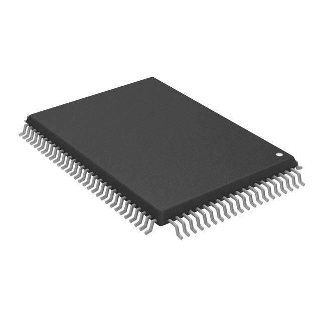
ICGOO电子元器件商城为您提供AT27C040-70JU由Atmel设计生产,在icgoo商城现货销售,并且可以通过原厂、代理商等渠道进行代购。 AT27C040-70JU价格参考。AtmelAT27C040-70JU封装/规格:存储器, EPROM - OTP 存储器 IC 4Mb (512K x 8) 并联 70ns 32-PLCC。您可以下载AT27C040-70JU参考资料、Datasheet数据手册功能说明书,资料中有AT27C040-70JU 详细功能的应用电路图电压和使用方法及教程。
Microchip Technology的AT27C040-70JU是一款EPROM(可擦除可编程只读存储器),其主要应用场景包括但不限于以下几种:

1. 嵌入式系统:AT27C040-70JU广泛应用于各种嵌入式控制系统中,如工业自动化设备、智能家居控制器和消费电子产品。它用于存储系统的启动代码、固件和关键配置数据,确保设备在上电后能够正确初始化并运行。

2. 通信设备:在通信领域,该芯片可用于存储网络设备的引导程序和配置参数。例如,在路由器、交换机等设备中,它可以保存设备启动所需的初始化指令和网络设置,确保设备能够快速恢复到正常工作状态。

3. 医疗设备:在医疗仪器中,AT27C040-70JU可以用来存储设备的校准数据和操作程序。由于其非易失性和可靠性,这款EPROM特别适合需要长时间稳定运行且对数据完整性要求较高的医疗应用,如监护仪、诊断设备等。

4. 汽车电子:在汽车行业中,该芯片常用于存储车辆控制单元(ECU)的固件和配置信息。它帮助汽车实现从冷启动到正常行驶过程中的各种功能控制,如发动机管理、安全气囊控制等。

5. 家电产品:在家电领域,AT27C040-70JU可用于存储洗衣机、空调等设备的操作程序和用户界面逻辑。通过预先写入的程序,这些家电可以在开机时自动加载正确的操作模式,提升用户体验。

总之,AT27C040-70JU凭借其高可靠性和稳定性,适用于多种需要非易失性存储的应用场景,尤其在需要长期保存关键数据和程序代码的情况下表现出色。
| 参数 | 数值 |
| 产品目录 | 集成电路 (IC)半导体 |
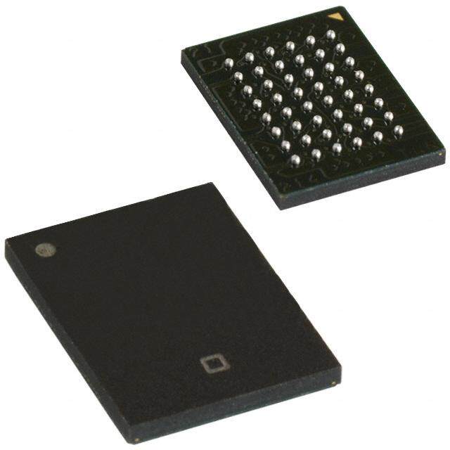
| 描述 | IC OTP 4MBIT 70NS 32PLCC可擦除可编程ROM 4Mb (512Kx8) OTP 5V 70ns |
| 产品分类 | |
| 品牌 | Atmel |
| 产品手册 | |
| 产品图片 |
|
| rohs | 符合RoHS无铅 / 符合限制有害物质指令(RoHS)规范要求 |
| 产品系列 | 内存,可擦除可编程ROM,Atmel AT27C040-70JU- |
| 数据手册 | |
| 产品型号 | AT27C040-70JU |
| 产品种类 | 可擦除可编程ROM |
| 供应商器件封装 | 32-PLCC |
| 其它名称 | AT27C04070JU |
| 包装 | 管件 |
| 商标 | Atmel |
| 存储器类型 | EPROM OTP |
| 存储容量 | 4 Mbit |
| 安装风格 | SMD/SMT |
| 封装/外壳 | 32-LCC(J 形引线) |
| 封装/箱体 | PLCC-32 |
| 工作温度 | -40°C ~ 85°C |
| 工作电流 | 100 uA |
| 工作电源电压 | 5 V |
| 工厂包装数量 | 32 |
| 接口 | 并联 |
| 接口类型 | Parallel |
| 最大工作温度 | + 85 C |
| 最小工作温度 | - 40 C |
| 标准包装 | 32 |
| 格式-存储器 | EPROMs |
| 电压-电源 | 4.5 V ~ 5.5 V |
| 电源电压-最大 | 5.5 V |
| 电源电压-最小 | 4.5 V |
| 类型 | OTP |
| 组织 | 512 k x 8 |
| 编程电压 | 13 V |
| 访问时间 | 70 ns |
| 输出启用访问时间 | 30 ns |
| 速度 | 70ns |


_renders/IS42S32800D-6BLI.jpg)

_renders/MR4A16BCYS35.jpg)

- 商务部:美国ITC正式对集成电路等产品启动337调查
- 曝三星4nm工艺存在良率问题 高通将骁龙8 Gen1或转产台积电
- 太阳诱电将投资9.5亿元在常州建新厂生产MLCC 预计2023年完工
- 英特尔发布欧洲新工厂建设计划 深化IDM 2.0 战略
- 台积电先进制程称霸业界 有大客户加持明年业绩稳了
- 达到5530亿美元!SIA预计今年全球半导体销售额将创下新高
- 英特尔拟将自动驾驶子公司Mobileye上市 估值或超500亿美元
- 三星加码芯片和SET,合并消费电子和移动部门,撤换高东真等 CEO
- 三星电子宣布重大人事变动 还合并消费电子和移动部门
- 海关总署:前11个月进口集成电路产品价值2.52万亿元 增长14.8%


PDF Datasheet 数据手册内容提取
Atmel AT27C040 4Mb (512K x 8) OTP, EPROM DATASHEET Features Fast read access time – 70ns Low-power CMOS operation 100μA max standby 30mA max active at 5MHz JEDEC standard packages 32-lead PDIP 32-lead PLCC 5V 10% supply High-reliability CMOS technology 2000V ESD protection 200mA latchup immunity Rapid programming algorithm – 100μs/byte (typical) CMOS- and TTL-compatible inputs and outputs Industrial temperature range Green (Pb/halide-free) packaging option 1. Description The Atmel® AT27C040 is a low-power, high-performance, 4,194,304-bit, One-Time Programmable, Read-Only Memory (OTP EPROM) organized as 512K by 8 bits. The AT27C040 requires only one 5V power supply in normal Read mode operation. Any byte can be accessed in less than 70ns, eliminating the need for speed reducing wait states on high-performance microprocessor systems. The Atmel scaled CMOS technology provides low active power consumption and fast programming. Power consumption is typically 8mA in active mode and less than 10μA in standby mode. The AT27C040 is available in a choice of industry standard, JEDEC-approved, PDIP and PLCC packages. The device features two-line control (CE, OE) to eliminate bus contention in high-speed systems. The AT27C040 has additional features to ensure high quality and efficient production use. The rapid programming algorithm reduces the time required to program the part and guarantees reliable programming. Programming time is typically only 100μs/byte. The integrated product identification code electronically identifies the device and manufacturer. This feature is used by industry standard programming equipment to select the proper programming algorithms and voltages. 0189J–EPROM–10/2012
2. Pin Configurations and Pinouts 32-lead PLCC 32-lead PDIP Pin Top view Top view Name Function VPP Peak to Peak Voltage 12 15 16 PP CC 18 17 A A A V V A A VPP 1 32 VCC A - A Address Inputs 0 18 A16 2 31 A18 4 3 2 1 2 1 0 O0 - O7 Outputs A7 5 3 3 329 A14 A15 3 30 A17 GND Ground A6 6 28 A13 A12 4 29 A14 A5 7 27 A8 A7 5 28 A13 CE Chip Enable A4 8 26 A9 A6 6 27 A8 OE Output Enable A3 9 25 A11 A5 7 26 A9 V Device Power Supply A2 10 24 OE A4 8 25 A11 CC A1 11 23 A10 A3 9 24 OE A0 12 22 CE A2 10 23 A10 O0 13 21 O7 A1 11 22 CE 14 15 16 17 18 19 20 A0 12 21 O7 O0 13 20 O6 1 2 D 3 4 5 6 O O N O O O O O1 14 19 O5 G O2 15 18 O4 GND 16 17 O3 3. Switching Considerations Switching between active and standby conditions via the Chip Enable (CE) pin may produce transient voltage excursions. Unless accommodated by the system design, these transients may exceed datasheet limits, resulting in device nonconformance. At a minimum, a 0.1μF, high-frequency, low inherent inductance, ceramic capacitor should be utilized for each device. This capacitor should be connected between the V and ground terminals of the device — as CC close to the device as possible. Additionally, to stabilize the supply voltage level on printed circuit boards with large EPROM arrays, a 4.7μF bulk electrolytic capacitor should be utilized, again connected between the V and ground CC terminals. This capacitor should be positioned as close as possible to the point where the power supply is connected to the array. 4. Block Diagram V Data Outputs CC GND O0 – O7 V PP OE OE, CE, and Output CE Program Logic Buffers Y Decoder Y-Gating A – A 0 18 Address Cell Matrix Inputs X Decoder Identification Atmel AT27C040 [DATASHEET] 2 0189J–EPROM–10/2012
5. Absolute maximum ratings* Temperature under bias-55°C to +125°C *Notice: Stresses beyond those listed under “Absolute Storage temperature . . . . . . . . . . . . .-65°C to +150°C maximum ratings” may cause permanent damage to the device. This is a stress rating only, and Voltage on any pin with functional operation of the device at these or any respect to ground. . . . . . . . . . . . . . . . . .-2.0V to +7.0V other conditions beyond those indicated in the operational sections of this specification is not Voltage on A with 9 implied. Exposure to absolute maximum rating respect to ground . . . . . . . . . . . . . . . .-2.0V to +14.0V conditions for extended periods may affect device V supply voltage with reliability. PP respect to ground. . . . . . . . . . . . . . . . .-2.0V to +14.0V 6. Elelectrical Characteristics 6.1 DC and AC characteristics Table 6-1. Operating modes Mode/Pin CE OE Ai V Outputs PP Read V V Ai X(1) D IL IL OUT Output Disable X V X X High Z IH Standby V X X X High Z IH Rapid Program(2) V V Ai V D IL IH PP IN PGM Verify X V Ai V D IL PP OUT PGM Inhibit V V X V High Z IH IH PP A = V (3) 9 H Product Identification(4) V V A = V or V X Identification Code IL IL 0 IH IL A – A = V 1 18 IL Notes: 1. X can be V or V . IL IH 2. Refer to programming characteristics. 3. V = 12.0 ± 0.5V. H 4. Two identifier bytes may be selected. All Ai inputs are held low (V ), except A , which is set to V , and A , IL 9 H 0 which is toggled low (V ) to select the manufacturer’s identification byte and high (V ) to select the device IL IH code byte. Atmel AT27C040 [DATASHEET] 3 0189J–EPROM–10/2012
6.2 DC and AC Operating Conditions for Read Operation Atmel AT27C040-70 Atmel AT27C040-90 Industrial Operating Temperature (Case) -40°C to 85°C -40°C to 85°C V Power Supply 5V 10% 5V 10% CC 6.3 DC and Operating Characteristics for Read Operation Symbol Parameter Condition Min Max Units I Input Load Current V = 0V to V 1 μA LI IN CC I Output Leakage Current V = 0V to V 5 μA LO OUT CC I (2) V (1) Read/Standby Current V = V 10 μA PP1 PP PP CC I (CMOS), CE = V 0.3V 100 μA SB1 CC I V (1) Standby Current SB CC1 I (TTL), CE = 2.0 to V + 0.5V 1 mA SB2 CC I V Active Current f = 5MHz, I = 0mA, CE = V 30 mA CC CC OUT IL V Input Low Voltage -0.6 0.8 V IL V Input High Voltage 2.0 V + 0.5 V IH CC V Output Low Voltage I = 2.1mA 0.4 V OL OL V Output High Voltage I = -400μA 2.4 V OH OH Notes: 1. V must be applied simultaneously with or before V , and removed simultaneously with or after V . CC PP PP 2. V may be connected directly to V , except during programming. The supply current would then be the PP CC sum of I and I . CC PP 6.4 AC Characteristics for Read Operation Atmel AT27C040 -70 -90 Symbol Parameter Condition Min Max Min Max Units CE = OE t (1) Address to Output Delay 70 90 ns ACC = V IL t (1) CE to Output Delay OE = V 70 90 ns CE IL t (1) OE to Output Delay CE = V 30 35 ns OE IL t (1) OE or CE High to Output Float; whichever occurred first. 20 20 ns DF Output Hold from Address, CE or OE; whichever occurred t 0 0 ns OH first. Note: 1. See AC waveforms for read operation. Atmel AT27C040 [DATASHEET] 4 0189J–EPROM–10/2012
Figure 6-1. AC Waveforms for Read Operation(1) Address Address Valid CE tCE tOE OE tDF tACC tOH High Z Output Output Valid Notes: 1. Timing measurement references are 0.8V and 2.0V. Input AC drive levels are 0.45V and 2.4V, unless otherwise specified. 2. OE may be delayed up to t – t after the falling edge of CE without impact on t . CE OE CE 3. OE may be delayed up to t – t after the address is valid without impact on t . ACC OE ACC 4. This parameter is only sampled, and is not 100% tested. 5. Output float is defined as the point when data is no longer driven. Figure 6-2. Input Test Waveforms and Measurement Levels 2.40V 2.00 AC AC Driving Measurement Levels Level 0.80 0.45V Figure 6-3. Output Test Load 1.3V (1N914) 3.3K OUTPUT PIN CL Table 6-2. Pin Capacitance f = 1MHz, T = 25°C (1) Symbol Typ Max Units Conditions C 4 8 pF V = 0V IN IN C 8 12 pF V = 0V OUT OUT Note: 1. Typical values for nominal supply voltage. This parameter is only sampled and is not 100% tested. Atmel AT27C040 [DATASHEET] 5 0189J–EPROM–10/2012
Figure 6-4. Programming Waveforms(1) Read Program (Verify) Address VIH Address Stable VIL tAS tOE tAH Data VIH Data Out Data In VIL Valid tDS tDH tDFP 13.0V V PP 5.0V tPRT tVPS 6.5V V CC 5.0V tVCS VIH CE VIL tPW tOES OE VIH VIL Notes: 1. The input timing reference is 0.8V for V and 2.0V for V . IL IH 2. t and t are characteristics of the device, but must be accommodated by the programmer. OE DFP 3. When programming the AT27C040, a 0.1μF capacitor is required across V and ground to suppress PP spurious voltage transients. Table 6-3. DC Programming Characteristics T = 25 ± 5°C, V = 6.5 ± 0.25V, V = 13.0 ± 0.25V. A CC PP Limits Symbol Parameter Test Conditions Min Max Units I Input Load Current V = V , V 10 μA LI IN IL IH V Input Low Level -0.6 0.8 V IL V Input High Level 2.0 V + 0.7 V IH CC V Output Low Voltage I = 2.1mA 0.4 V OL OL V Output High Voltage I = -400μA 2.4 V OH OH I V Supply Current (Program And Verify) 40 mA CC2 CC I V Supply Current CE = V 20 mA PP2 PP IL V A Product Identification Voltage 11.5 12.5 V ID 9 Atmel AT27C040 [DATASHEET] 6 0189J–EPROM–10/2012
Table 6-4. AC Programming Characteristics T = 25 5°C, V = 6.5 0.25V, V = 13.0 0.25V A CC PP Limits Symbol Parameter Test Conditions(1) Min Max Units t Address Setup Time 2 μs AS t OE Setup Time 2 μs OES Input rise and fall times: t Data Setup Time 2 μs DS (10% to 90%) 20ns t Address Hold Time 0 μs AH Input pulse levels: t Data Hold Time 2 μs DH 0.45V to 2.4V t OE High to Output Float Delay(2) 0 130 ns DFP t V Setup Time Input timing reference level: 2 μs VPS pp 0.8V to 2.0V t V Setup Time 2 μs VCS cc t CE Program Pulse Width(3) 95 105 μs PW Output timing reference level: t Data Valid from OE(2) 0.8V to 2.0V 150 ns OE V Pulse Rise Time During t PP 50 ns PRT Programming Notes: 1. V must be applied simultaneously with or before V and removed simultaneously with or after V . CC PP PP 2. This parameter is only sampled, and is not 100% tested. Output float is defined as the point where data is no longer driven. See timing diagram. 3. Program pulse width tolerance is 100μs 5%. Table 6-5. Atmel AT27C040 Integrated Product Identification Code Pins Codes A O O O O O O O O Hex Data 0 7 6 5 4 3 2 1 0 Manufacturer 0 0 0 0 1 1 1 1 0 1E Device Type 1 0 0 0 0 1 0 1 1 0B Atmel AT27C040 [DATASHEET] 7 0189J–EPROM–10/2012
7. Rapid programming algorithm A 100μs CE pulse width is used to program. The address is set to the first location. V is raised to 6.5V and V is CC PP raised to 13.0V. Each address is first programmed with one 100μs CE pulse without verification. Then a verification/reprogramming loop is executed for each address. In the event a byte fails to pass verification, up to ten successive 100μs pulses are applied with a verification after each pulse. If the byte fails to verify after ten pulses have been applied, the part is considered failed. After the byte verifies properly, the next address is selected until all have been checked. V is then lowered to 5.0V and V to 5.0V. All bytes are read again and compared with the original data to PP CC determine if the device passes or fails. Figure 7-1. Rapid Programming Algorithm Start ADDR = First Location V = 6.5V CC V = 13.0V PP Program One 100μs Pulse Increment No Last Address ADDR? Yes ADDR = First Location Increment X = 0 Address No Last Pass Fail Verify Increment ADDR? Byte Yes No Program One 100μs Pulse X = 10? Yes V = 6.5V CC V = 13.0V PP Compare Fail Device All Bytes Failed to Original Data Pass Device Passed Atmel AT27C040 [DATASHEET] 8 0189J–EPROM–10/2012
8. Ordering Information Green Package Option (Pb/Halide-free) I (mA) CC Atmel Ordering Code Package t (ns) Active Standby Lead Finish Operation Range ACC AT27C040-70JU 32J Industrial 70 30 0.1 Matte Tin (-40C to 85C) AT27C040-70PU 32P6 AT27C040-90JU 32J Industrial 90 30 0.1 Matte Tin (-40C to 85C) AT27C040-90PU 32P6 Package Type 32J 32-lead, plastic, J-leaded Chip Carrier (PLCC) 32P6 32-lead, 0.600" wide, plastic, Dual Inline (PDIP) Atmel AT27C040 [DATASHEET] 9 0189J–EPROM–10/2012
9. Package information 9.1 32J — 32-lead PLCC 1.14(0.045) X 45° PIN NO. 1 1.14(0.045) X 45° IDENTIFIER 0.318(0.0125) 0.191(0.0075) E1 E B1 E2 B e A2 D1 A1 D A 0.51(0.020)MAX 45° MAX (3X) COMMON DIMENSIONS (Unit of measure = mm) SYMBOL MIN NOM MAX NOTE D2 A 3.175 – 3.556 A1 1.524 – 2.413 A2 0.381 – – D 12.319 – 12.573 D1 11.354 – 11.506 Note 2 D2 9.906 – 10.922 Notes: 1. This package conforms to JEDEC reference MS-016, Variation AE. E 14.859 – 15.113 2. Dimensions D1 and E1 do not include mold protrusion. Allowable protrusion is .010"(0.254mm) per side. Dimension D1 E1 13.894 – 14.046 Note 2 and E1 include mold mismatch and are measured at the extreme E2 12.471 – 13.487 material condition at the upper or lower parting line. 3. Lead coplanarity is 0.004" (0.10mm) maximum. B 0.660 – 0.813 B1 0.330 – 0.533 e 1.270 TYP 10/04/01 TITLE DRAWING NO. REV. Package Drawing Contact: 32J, 32-lead, Plastic J-leaded Chip Carrier (PLCC) packagedrawings@atmel.com 32J B Atmel AT27C040 [DATASHEET] 10 0189J–EPROM–10/2012
9.2 32P6 — 32-lead PDIP 32 17 E1 1 16 D e A BASE PLANE -C- SEATING PLANE A1 b2 L .015 E b j 0.10m C GAGE PLANE See Z Z Lead Detail COMMON DIMENSIONS (UNIT OF MEASURE=MM) Symbol Min. Nom. Max. Note C A - - 4.826 L A1 0.381 - - eA b 0.356 - 0.558 eC c b2 1.041 - 1.651 Lead Detail eB c 0.203 - 0.381 D 41.783 - 42.291 Note 1 E 15.240 - 15.875 E1 13.462 - 13.970 Note 1 Notes: L 3.048 - 3.556 1. Dimensions D and E1 do not include mold Flash or e 2.54 BSC Protrusion. Mold Flash or Protrusion shall not exceed eA 15.24 BSC 0.25 mm (0.010"). eB - - 17.78 eC 0.000 - 1.524 11/28/11 TITLE GPC DRAWING NO. REV. 32P6, 32-lead, 0.600”/15.24 mm Wide Plastic Dual Inline Package (PDIP) PLU 32P6 C Package Drawing Contact: packagedrawings@atmel.com Atmel AT27C040 [DATASHEET] 11 0189J–EPROM–10/2012
10. Revision History Doc. Rev. Date Comments Update 32P6 package outline drawing. 0189J 10/2012 Update template and Atmel logo. Remove TSOP package. 0189I 04/2011 Add lead finish to ordering information. 0189H 12/2007 Datasheet revision. Atmel AT27C040 [DATASHEET] 12 0189J–EPROM–10/2012
Atmel Corporation Atmel Asia Limited Atmel Munich GmbH Atmel Japan G.K. 1600 Technology Drive Unit 01-5 & 16, 19F Business Campus 16F Shin-Osaki Kangyo Bldg San Jose, CA 95110 BEA Tower, Millennium City 5 Parkring 4 1-6-4 Osaki, Shinagawa-ku USA 418 Kwun Tong Roa D-85748 Garching b. Munich Tokyo 141-0032 Tel: (+1) (408) 441-0311 Kwun Tong, Kowloon GERMANY JAPAN Fax: (+1) (408) 487-2600 HONG KONG Tel: (+49) 89-31970-0 Tel: (+81) (3) 6417-0300 www.atmel.com Tel: (+852) 2245-6100 Fax: (+49) 89-3194621 Fax: (+81) (3) 6417-0370 Fax: (+852) 2722-1369 © 2012 Atmel Corporation. All rights reserved. / Rev.: 0189J–EPROM–10/2012 Atmel®, logo and combinations thereof, and others are registered trademarks or trademarks of Atmel Corporation or its subsidiaries. Other terms and product names may be trademarks of others. Disclaimer: The information in this document is provided in connection with Atmel products. No license, express or implied, by estoppel or otherwise, to any intellectual property right is granted by this document or in connection with the sale of Atmel products. EXCEPT AS SET FORTH IN THE ATMEL TERMS AND CONDITIONS OF SALES LOCATED ON THE ATMEL WEBSITE, ATMEL ASSUMES NO LIABILITY WHATSOEVER AND DISCLAIMS ANY EXPRESS, IMPLIED OR STATUTORY WARRANTY RELATING TO ITS PRODUCTS INCLUDING, BUT NOT LIMITED TO, THE IMPLIED WARRANTY OF MERCHANTABILITY, FITNESS FOR A PARTICULAR PURPOSE, OR NON-INFRINGEMENT. IN NO EVENT SHALL ATMEL BE LIABLE FOR ANY DIRECT, INDIRECT, CONSEQUENTIAL, PUNITIVE, SPECIAL OR INCIDENTAL DAMAGES (INCLUDING, WITHOUT LIMITATION, DAMAGES FOR LOSS AND PROFITS, BUSINESS INTERRUPTION, OR LOSS OF INFORMATION) ARISING OUT OF THE USE OR INABILITY TO USE THIS DOCUMENT, EVEN IF ATMEL HAS BEEN ADVISED OF THE POSSIBILITY OF SUCH DAMAGES. Atmel makes no representations or warranties with respect to the accuracy or completeness of the contents of this document and reserves the right to make changes to specifications and products descriptions at any time without notice. Atmel does not make any commitment to update the information contained herein. Unless specifically provided otherwise, Atmel products are not suitable for, and shall not be used in, automotive applications. Atmel products are not intended, authorized, or warranted for use as components in applications intended to support or sustain life.
Mouser Electronics Authorized Distributor Click to View Pricing, Inventory, Delivery & Lifecycle Information: M icrochip: AT27C040-70TC AT27C040-15RC AT27C040-15JC AT27C040-15PC AT27C040-15PI AT27C040-15TC AT27C040-12JC AT27C040-90PC AT27C040-90JI AT27C040-70JC AT27C040-70PI AT27C040-90PI AT27C040- 70PU AT27C040-90PU AT27C040-70JI AT27C040-70JU AT27C040-90JU AT27C040-70TI AT27C040-90TI AT27C040-70TU AT27C040-90TU AT27C040-12PC AT27C040-90JU-T AT27C040-70JU-T