 Datasheet下载
- 型号: 7005L55PF
- 制造商: Integrated Device Technology
- 库位|库存: xxxx|xxxx
- 要求:
| 数量阶梯 | 香港交货 | 国内含税 |
| +xxxx | $xxxx | ¥xxxx |
查看当月历史价格
查看今年历史价格
7005L55PF产品简介:
ICGOO电子元器件商城为您提供7005L55PF由Integrated Device Technology设计生产,在icgoo商城现货销售,并且可以通过原厂、代理商等渠道进行代购。 7005L55PF价格参考。Integrated Device Technology7005L55PF封装/规格:存储器, SRAM - 双端口,异步 存储器 IC 64Kb (8K x 8) 并联 55ns 64-TQFP(14x14)。您可以下载7005L55PF参考资料、Datasheet数据手册功能说明书,资料中有7005L55PF 详细功能的应用电路图电压和使用方法及教程。
IDT(Integrated Device Technology Inc.)的7005L55PF是一款属于存储器类别中的先进先出存储器(FIFO),主要用于需要高速数据缓冲和时序管理的场景。其典型应用场景包括:

1. 通信设备:在路由器、交换机等网络设备中,用于缓存数据包,平衡不同速率的数据流,确保数据传输的稳定性和高效性。

2. 工业控制系统:用于工业自动化系统中,处理来自传感器或执行器的数据流,实现高速数据采集与传输的缓冲管理。

3. 测试与测量设备:在示波器、逻辑分析仪等测试仪器中,用于暂存采集到的数据,以便后续处理与分析。

4. 图像处理系统:用于图像采集与处理模块中,缓存图像数据流,确保图像传输过程中不丢失数据。

5. 嵌入式系统:在需要高速数据缓冲的嵌入式系统中,作为临时存储单元,协调不同模块间的数据传输。

该芯片具有高速访问能力、低功耗设计,适用于需要高可靠性和高性能数据缓冲的场合。
| 参数 | 数值 |
| 品牌 | IDT |
| 产品目录 | 半导体 |
| 描述 | 静态随机存取存储器 8K x 8 Dual-Port RAM |
| 产品分类 | 集成电路 - IC |
| 产品手册 | http://www.idt.com/document/dst/7005-data-sheet |
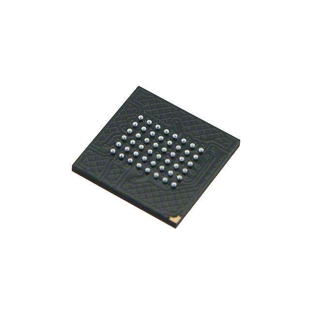
| 产品图片 |
|
| rohs | 否 |
| 产品系列 | 内存,静态随机存取存储器,IDT 7005L55PF |
| 产品型号 | 7005L55PF |
| 产品种类 | 静态随机存取存储器 |
| 商标 | IDT |
| 存储容量 | 64 kbit |
| 存储类型 | SDR |
| 安装风格 | SMD/SMT |
| 封装 | Tube |
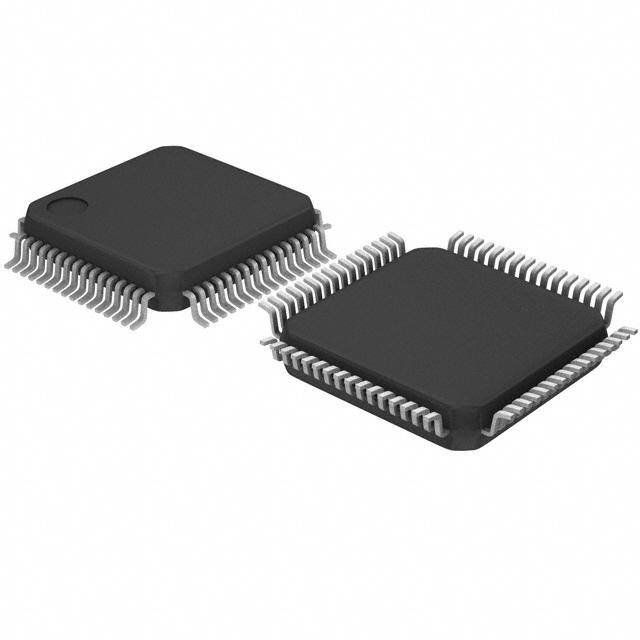
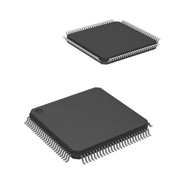
| 封装/箱体 | TQFP-64 |
| 工厂包装数量 | 45 |
| 接口 | Parallel |
| 最大工作温度 | + 70 C |
| 最大工作电流 | 210 mA |
| 最小工作温度 | 0 C |
| 电源电压-最大 | 5.5 V |
| 电源电压-最小 | 4.5 V |
| 类型 | Asynchronous |
| 系列 | 7005 |
| 组织 | 8 k x 8 |
| 访问时间 | 55 ns |
| 零件号别名 | 7005 IDT7005L55PF |


- 商务部:美国ITC正式对集成电路等产品启动337调查
- 曝三星4nm工艺存在良率问题 高通将骁龙8 Gen1或转产台积电
- 太阳诱电将投资9.5亿元在常州建新厂生产MLCC 预计2023年完工
- 英特尔发布欧洲新工厂建设计划 深化IDM 2.0 战略
- 台积电先进制程称霸业界 有大客户加持明年业绩稳了
- 达到5530亿美元!SIA预计今年全球半导体销售额将创下新高
- 英特尔拟将自动驾驶子公司Mobileye上市 估值或超500亿美元
- 三星加码芯片和SET,合并消费电子和移动部门,撤换高东真等 CEO
- 三星电子宣布重大人事变动 还合并消费电子和移动部门
- 海关总署:前11个月进口集成电路产品价值2.52万亿元 增长14.8%
/IS61LPS102418B-200B3LI.jpg)
_renders/IS42S32800D-6BLI.jpg)


PDF Datasheet 数据手册内容提取
HIGH-SPEED IDT7005S/L 8K x 8 DUAL-PORT STATIC RAM LEAD FINISH (SnPb) ARE IN EOL PROCESS - LAST TIME BUY EXPIRES JUNE 15, 2018 Features ◆ True Dual-Ported memory cells which allow simultaneous ◆ M/S = H for BUSY output flag on Master, reads of the same memory location M/S = L for BUSY input on Slave ◆ High-speed access ◆ Interrupt Flag – Military: 20/25/35/55/70ns (max.) ◆ On-chip port arbitration logic – Industrial: 20/35/55ns (max.) ◆ Full on-chip hardware support of semaphore signaling – Commercial:15/17/20/25/35/55ns (max.) between ports ◆ Low-power operation ◆ Fully asynchronous operation from either port – IDT7005S ◆ Devices are capable of withstanding greater than 2001V Active: 750mW (typ.) electrostatic discharge Standby: 5mW (typ.) ◆ Battery backup operation—2V data retention – IDT7005L ◆ TTL-compatible, single 5V (±10%) power supply Active: 700mW (typ.) ◆ Available in 68-pin PGA, PLCC and a 64-pin thin quad Standby: 1mW (typ.) flatpack ◆ IDT7005 easily expands data bus width to 16 bits or more ◆ Industrial temperature range (-40°C to +85°C) is available for using the Master/Slave select when cascading more than selected speeds one device ◆ Green parts available, see ordering information Functional Block Diagram OEL OER CEL CER R/WL R/WR I/O0L-I/O7L I/O0R-I/O7R I/O I/O Control Control BUSYL(1,2) BUSYR(1,2) A12L Address MEMORY Address A12R A0L Decoder ARRAY Decoder A0R 13 13 ARBITRATION CEL INTERRUPT CER OEL SEMAPHORE OER R/WL LOGIC R/WR SEML M/S SEMR INTL(2) INTR(2) 2738drw01 NOTES: 1. (MASTER): BUSY is output; (SLAVE): BUSY is input. 2. BUSY outputs and INT outputs are non-tri-stated push-pull. MARCH 2018 1 ©2018 Integrated Device Technology, Inc. DSC 2738/19
IDT7005S/L High-Speed 8K x 8 Dual-Port Static RAM Military, Industrial and Commercial Temperature Ranges Description The IDT7005 is a high-speed 8K x 8 Dual-Port Static RAM. The IDT7005 is designed to be used as a stand-alone 64K-bit Dual-Port RAM Fabricated using CMOS high-performance technology, these de- or as a combination MASTER/SLAVE Dual-Port RAM for 16-bit-or- vices typically operate on only 750mW of power. Low-power (L) versions more word systems. Using the IDT MASTER/SLAVE Dual-Port RAM offer battery backup data retention capability with typical power consump- approach in 16-bit or wider memory system applications results in full- tion of 500µW from a 2V battery. speed, error-free operation without the need for additional discrete logic. The IDT7005 is packaged in a ceramic 68-pin PGA, 68-pin PLCC This device provides two independent ports with separate control, and a 64-pin thin quad flatpack, (TQFP). Military grade product is address, and I/O pins that permit independent, asynchronous access for manufactured in compliance with MIL-PRF-38535 QML making it ideally reads or writes to any location in memory. An automatic power down suited to military temperature applications demanding the highest level of feature controlled by CE permits the on-chip circuitry of each port to enter performance and reliability. a very low standby power mode. Pin Configurations(1,2,3) I/O6RI/O5RI/O4RI/O3RVCC I/O2RI/O1RI/O0RGND VCC I/O7L I/O6L GND I/O5L I/O4L I/O3L I/O2L I/O7R 272625 2423 2221 2019 1817 1615 141312 11109 I/O1L N/C 28 8 I/O0L OER 29 7 N/C R/WR 30 6 OEL SEMR 31 5 R/WL CER 32 4 SEML N/C 33 3 CEL N/C 34 7005J 2 N/C GND 35 J68(4) 1 N/C A12R 36 68 VCC A11R 37 67 A12L A10R 38 66 A11L A9R 39 65 A10L A8R 40 64 A9L A7R 41 63 A8L A6R 42 62 A7L A5R 43 61 A6L 4445 4647 4849 5051 5253 5455 565758 5960 R R R R R R R S D L L L L L L L L 2738 drw 02 A4A3A2A1A0INTBUSYM/GNBUSYINTA0A1A2A3A4A5 A4L A3L A2L A1L A0L INTL BUSYL GND M/ S BUSYR INTR A0R A1R A2R A3R A4R 4847 464544 43 424140 39 383736353433 A5L 49 32 A5R A6L 50 31 A6R A7L 51 30 A7R A8L 52 29 A8R A9L 53 28 A9R A10L 54 27 A10R A11L 55 26 A11R A12L 56 7005 25 A12R VCC 57 PN64(4) 24 GND N/C 58 23 N/C CEL 59 22 CER SEML 60 21 SEMR R/WL 61 20 R/WR NOTES: OEL 62 19 OER 1. All VCC pins must be connected to power supply. I/O0L 63 18 I/O7R 2. All GND pins must be connected to ground supply. I/O1L 64 17 I/O6R 1 2 3 4 5 6 7 8 9 101112 131415 16 3. J68 package body is approximately .95 in x .95 in x .12 in. PN64 package body is approximately 14mm x 14mm x 1.4mm. 2738 drw 03 4. This package code is used to reference the package diagram. I/O2L I/O3L I/O4L I/O5L GND I/O6L I/O7L VCC GND I/O0R I/O1R I/O2R VCC I/O3R I/O4R I/O5R 6.242
IDT7005S/L High-Speed 8K x 8 Dual-Port Static RAM Military, Industrial and Commercial Temperature Ranges Pin Configurations(1,2,3) (con't.) 51 50 48 46 44 42 40 38 36 11 A5L A4L A2L A0L BUSYL M/S INTR A1R A3R 53 52 49 47 45 43 41 39 37 35 34 10 A7L A6L A3L A1L INTL GND BUSYR A0R A2R A4R A5R 55 54 32 33 09 A9L A8L A7R A6R 57 56 30 31 08 A11L A10L A9R A8R 59 58 28 29 07 VCC A12L A11R A10R 7005G 61 60 G68(4,5) 26 27 06 N/C N/C GND A12R 63 62 24 25 05 SEML CEL N/C N/C 65 64 22 23 04 OEL R/WL SEMR CER 67 66 20 21 03 I/O0L N/C OER R/WR 68 1 3 5 7 9 11 13 15 18 19 02 I/O1L I/O2L I/O4L GND I/O7L GND I/O1R VCC I/O4R I/O7R N/C 2 4 6 8 10 12 14 16 17 01 I/O3L I/O5L I/O6L VCC I/O0R I/O2R I/O3R I/O5R I/O6R A B C D E F G H J K L INDEX 2738 drw04 NOTES: 1. All VCC pins must be connected to power supply. Pin Names 2. All GND pins must be connected to ground supply. 3. Package body is approximately 1.18in x 1.18in x .16in. Left Port Right Port Names 4. This package code is used to reference the package diagram. 5. This text does not indicate oriention of the actual part-marking CEL CER Chip Enable R/WL R/WR Read/Write Enable OEL OER Output Enable A0L - A12L A0R - A12R Address I/O0L - I/O7L I/O0R - I/O7R Data Input/Output SEML SEMR Semaphore Enable INTL INTR Interrupt Flag BUSYL BUSYR Busy Flag M/S Master or Slave Select VCC Power GND Ground 2738 tbl 01 6.342
IDT7005S/L High-Speed 8K x 8 Dual-Port Static RAM Military, Industrial and Commercial Temperature Ranges Truth Table I: Non-Contention Read/Write Control Inputs(1) Outputs CE R/W OE SEM I/O0-7 Mode H X X H High-Z Deselected: Power-Down L L X H DATAIN Write to Memory L H L H DATAOUT Read Memory X X H X High-Z Outputs Disabled NOTE: 2738 tbl 02 1. A0L – A12L is not equal to A0R – A12R Truth Table II: Semaphore Read/Write Control(1) Inputs(1) Outputs CE R/W OE SEM I/O0-7 Mode H H L L DATAOUT Read in Semaphore Flag Data Out H ↑ X L DATAIN Write I/Oo into Semaphore Flag L X X L ____ Not Allowed NOTE: 2738 tbl 03 1. There are eight semaphore flags written to via I/O0 and read from I/O0 - I/O7. These eight semaphores are addressed by A0 - A2. Absolute Maximum Ratings(1) Maximum Operating Temperature Commercial and Supply Voltage(1,2) Symbol Rating & Industrial Military Unit Ambient VTERM(2) Terminal Voltage -0.5 to +7.0 -0.5 to +7.0 V Grade Temperature GND Vcc with Respect to GND Military -55OC to+125OC 0V 5.0V + 10% TBIAS Temperature Under -55 to +125 -65 to +135 oC Commercial 0OC to +70OC 0V 5.0V + 10% Bias Industrial -40OC to +85OC OV 5.0V + 10% TSTG Storage -65 to +150 -65 to +150 oC Temperature NOTES: 2738 tbl 05 IOUT DC Output Current 50 50 mA 12. TInhdisu sitsr iathl ete pmapraemraetuterer : TfAo.r Tshpies ciisfi ct hsep e"iendssta, npt aocnk"a gceass ea tnedm ppoewraetursre .contact your sales office. 2738 tbl 04 NOTES: 1. Stresses greater than those listed under ABSOLUTE MAXIMUM RATINGS may cause permanent damage to the device. This is a stress rating only and functional Recommended DC Operating operation of the device at these or any other conditions above those indicated in the operational sections of this specification is not implied. Exposure to Conditions absolute maximum rating conditions for extended periods may affect reliability. Symbol Parameter Min. Typ. Max. Unit 2. VTERM must not exceed Vcc + 10% for more than 25% of the cycle time or 10% maximum, and is limited to < 20mA for the period of VTERM > Vcc + 10%. VCC Supply Voltage 4.5 5.0 5.5 V GND Ground 0 0 0 V Capacitance(1) (TA = +25°C, f = 1.0MHz) VIH Input High Voltage 2.2 ____ 6.0(2) V Symbol Parameter Conditions(2) Max. Unit VIL Input Low Voltage -0.5(1) ____ 0.8 V CIN Input Capacitance VIN = 3dV 9 pF 2738 tbl 06 NOTES: COUT Output Capacitance VOUT = 3dV 10 pF 1. VIL > -1.5V for pulse width less than 10ns. 2. VTERM must not exceed Vcc + 10%. 2738 tbl 07 NOTES: 1. These parameters are determined by device characterization but are not production tested (TQFP Package only). 2. 3dV references the interpolated capacitance when the input and output signals switch from 0V to 3V or from 3V to 0V. 6.442
IDT7005S/L High-Speed 8K x 8 Dual-Port Static RAM Military, Industrial and Commercial Temperature Ranges DC Electrical Characteristics Over the 0perating Temperature and Supply Voltage Range (VCC = 5.0V ± 10%) 7005S 7005L Symbol Parameter Test Conditions Min. Max. Min. Max. Unit |ILI| Input Leakage Current(1) VCC = 5.5V, VIN = 0V to VCC ___ 10 ___ 5 µA |ILO| Output Leakage Current CE = VIH, VOUT = 0V to VCC ___ 10 ___ 5 µA VOL Output Low Voltage IOL = +4mA ___ 0.4 ___ 0.4 V VOH Output High Voltage IOH = -4mA 2.4 ___ 2.4 ___ V 2738 tbl 08 NOTE: 1. At Vcc < 2.0V input leakages are undefined. Data Retention Characteristics Over All Temperature Ranges (L Version Only) (VLC = 0.2V, VHC = VCC - 0.2V) Symbol Parameter Test Condition Min. Typ.(1) Max. Unit VDR VCC for Data Retention VCC = 2V 2.0 ___ ___ V ICCDR Data Retention Current CE > VHC Mil. & Ind. ___ 100 4000 µA VIN > VHC or < VLC Com'l. ___ 100 1500 tCDR(3) Chip Deselect to Data Retention Time SEM > VHC 0 ___ ___ ns tR(3) Operation Recovery Time tRC(2) ___ ___ ns NOTES: 2738 tbl 09 1. TA = +25°C, VCC = 2V, and are not production tested. 2. tRC = Read Cycle Time 3. This parameter is guaranteed by characterization, but is not production tested. Data Retention Waveform DATARETENTIONMODE VCC 4.5V VDR> 2V 4.5V tCDR tR VDR CE VIH VIH 2738drw05 6.542
IDT7005S/L High-Speed 8K x 8 Dual-Port Static RAM Military, Industrial and Commercial Temperature Ranges DC Electrical Characteristics Over the Operating Temperature and Supply Voltage Range(1) (VCC = 5.0V ± 10%) 7005X15 7005X17 7005X20 7005X25 Com'l Only Com'l Only Com'l, Ind Com'l & & Military Military Symbol Parameter Test Condition Version Typ.(2) Max. Typ.(2) Max. Typ.(2) Max. Typ.(2) Max. Unit ICC Dynamic Operating Current CE = VIL, Outputs Disabled COM'L S 170 310 170 310 160 290 155 265 mA (Both Ports Active) SEM = VIH L 160 260 160 260 150 240 145 220 f = fMAX(3) MIL & S ____ ____ ____ ____ 160 370 155 340 IND L ____ ____ ____ ____ 150 320 145 280 ISB1 Standby Current CEL = CER = VIH COM'L S 20 60 20 60 20 60 16 60 mA (Both Ports - TTL SEMR = SEML = VIH L 10 60 10 50 10 50 10 50 Level Inputs) f = fMAX(3) MIL & S ____ ____ ____ ____ 20 90 16 80 IND L ____ ____ ____ ____ 10 70 10 65 ISB2 Standby Current CE"A" = VIL and CE"B" = VIH(5) COM'L S 105 190 105 190 95 180 90 170 mA (One Port - TTL Active Port Outputs Disabled L 95 160 95 160 85 150 80 140 Level Inputs) f=fMAX(3) SEMR = SEML = VIH MIL & S ____ ____ ____ ____ 95 240 90 215 IND L ____ ____ ____ ____ 85 210 80 180 ISB3 Full Standby Current (Both Both Ports CEL and COM'L S 1.0 15 1.0 15 1.0 15 1.0 15 mA Ports - All CMOS Level CER > VCC - 0.2V L 0.2 5 0.2 5 0.2 5 0.2 5 Inputs) VIN > VCC - 0.2V or VIN < 0.2V, f = 0(4) MIL & S ____ ____ ____ ____ 1.0 30 1.0 30 SEMR = SEML > VCC - 0.2V IND L ____ ____ ____ ____ 0.2 10 0.2 10 ISB4 Full Standby Current CE"A" < 0.2V and COM'L S 100 170 100 170 90 155 85 145 mA (One Port - All CE"B" > VCC - 0.2V(5) L 90 140 90 140 80 130 75 120 CMOS Level Inputs) SEMR = SEML > VCC - 0.2V VIN > VCC - 0.2V or VIN < 0.2V MIL & S ____ ____ ____ ____ 90 225 85 200 Active Port Outputs Disabled IND L ____ ____ ____ ____ 80 200 75 170 f = fMAX(3) 2738 tbl 10 7005X35 7005X55 7005X70 Com'l, Ind Com'l, Ind Military & Military & Military Only Symbol Parameter Test Condition Version Typ.(2) Max. Typ.(2) Max. Typ.(2) Max. Unit ICC Dynamic Operating CE = VIL, Outputs Disabled COM'L S 150 250 150 250 ____ ____ mA Current SEM = VIH L 140 210 140 210 ____ ____ (Both Ports Active) f = fMAX(3) MIL & S 150 300 150 300 140 300 IND L 140 250 140 250 130 250 ISB1 Standby Current CEL = CER = VIH COM'L S 13 60 13 60 ____ ____ mA (Both Ports - TTL SEMR = SEML = VIH L 10 50 10 50 ____ ____ Level Inputs) f = fMAX(3) MIL & S 13 80 13 80 10 80 IND L 10 65 10 65 8 65 ISB2 Standby Current CE"A" = VIL and CE"B" = VIH(5) COM'L S 85 155 85 155 ____ ____ mA (One Port - TTL Active Port Outputs Disabled L 75 130 75 130 ____ ____ Level Inputs) f=fMAX(3) SEMR = SEML = VIH MIL & S 85 190 85 190 80 190 IND L 75 160 75 160 70 160 ISB3 Full Standby Current Both Ports CEL and COM'L S 1.0 15 1.0 15 ____ ____ mA (Both Ports - All CER > VCC - 0.2V L 0.2 5 0.2 5 ____ ____ CMOS Level Inputs) VIN > VCC - 0.2V or VIN < 0.2V, f = 0(4) MIL & S 1.0 30 1.0 30 1.0 30 SEMR = SEML > VCC - 0.2V IND L 0.2 10 0.2 10 0.2 10 ISB4 Full Standby Current CE"A" < 0.2V and COM'L S 80 135 80 135 ____ ____ mA (One Port - All CE"B" > VCC - 0.2V(5) L 70 110 70 110 ____ ____ CMOS Level Inputs) SEMR = SEML > VCC - 0.2V VIN > VCC - 0.2V or VIN < 0.2V MIL & S 80 175 80 175 75 175 Active Port Outputs Disabled IND L 70 150 70 150 65 150 f = fMAX(3) 2738 tbl 11 NOTES: 1. 'X' in part number indicates power rating (S or L) 2. VCC = 5V, TA = +25°C and are not production tested. ICC DC = 120mA (typ) 3. At f = fMAX, address and I/O'S are cycling at the maximum frequency read cycle of 1/tRC, and using “AC Test Conditions” of input levels of GND to 3V. 4. f = 0 means no address or control lines change. 5. Port "A" may be either left or right port. Port "B" is the port opposite port "A". 6.642
IDT7005S/L High-Speed 8K x 8 Dual-Port Static RAM Military, Industrial and Commercial Temperature Ranges AC Test Conditions 5V 5V Input Pulse Levels GND to 3.0V 1250Ω 1250Ω Input Rise/Fall Times 5ns Max. DATAOUT Input Timing Reference Levels 1.5V BUSY DATAOUT Output Reference Levels 1.5V INT 775Ω 30pF 775Ω 5pF* Output Load Figures 1 and 2 2738 tbl 12 2738drw06 Figure 1. AC Output Test Load Figure 2. Output Test Load (For tLZ, tHZ, tWZ, tOW) *Including scope and jig AC Electrical Characteristics Over the Operating Temperature and Supply Voltage Range(4) 7005X15 7005X17 7005X20 7005X25 Com'l Only Com'l Only Com'l, Ind Com'l & & Military Military Symbol Parameter Min. Max. Min. Max. Min. Max. Min. Max. Unit READ CYCLE tRC Read Cycle Time 15 ____ 17 ____ 20 ____ 25 ____ ns tAA Address Access Time ____ 15 ____ 17 ____ 20 ____ 25 ns tACE Chip Enable Access Time(3) ____ 15 ____ 17 ____ 20 ____ 25 ns tAOE Output Enable Access Time ____ 10 ____ 10 ____ 12 ____ 13 ns tOH Output Hold from Address Change 3 ____ 3 ____ 3 ____ 3 ____ ns tLZ Output Low-Z Time(1,2) 3 ____ 3 ____ 3 ____ 3 ____ ns tHZ Output High-Z Time(1,2) ____ 10 ____ 10 ____ 12 ____ 15 ns tPU Chip Enable to Power Up Time(2,5) 0 ____ 0 ____ 0 ____ 0 ____ ns tPD Chip Disable to Power Down Time(2,5) ____ 15 ____ 17 ____ 20 ____ 25 ns tSOP Semaphore Flag Update Pulse (OE or SEM) 10 ____ 10 ____ 10 ____ 10 ____ ns tSAA Semaphore Address Access Time ____ 15 ____ 17 ____ 20 ____ 25 ns 2738 tbl 13a 7005X35 7005X55 IDT7005X70 Com'l, Ind Com'l, Ind Military & Military & Military Only Symbol Parameter Min. Max. Min. Max. Min. Max. Unit READ CYCLE tRC Read Cycle Time 35 ____ 55 ____ 70 ____ ns tAA Address Access Time ____ 35 ____ 55 ____ 70 ns tACE Chip Enable Access Time(3) ____ 35 ____ 55 ____ 70 ns tAOE Output Enable Access Time ____ 20 ____ 30 ____ 35 ns tOH Output Hold from Address Change 3 ____ 3 ____ 3 ____ ns tLZ Output Low-Z Time(1,2) 3 ____ 3 ____ 3 ____ ns tHZ Output High-Z Time(1,2) ____ 15 ____ 25 ____ 30 ns tPU Chip Enable to Power Up Time(2,5) 0 ____ 0 ____ 0 ____ ns tPD Chip Disable to Power Down Time(2,5) ____ 35 ____ 50 ____ 50 ns tSOP Semaphore Flag Update Pulse (OE or SEM) 15 ____ 15 ____ 15 ____ ns tSAA Semaphore Address Access Time ____ 35 ____ 55 ____ 70 ns NOTES: 2738 tbl 13b 1. Transition is measured 0mV from Low or High impedance voltage with load (Figures 1 and 2). 2. This parameter is guaranteed but not production tested. 3. To access RAM, CE = VIL and SEM = VIH. To access semaphore, CE = VIH and SEM = VIL. 4. 'X' in part number indicates power rating (S or L). 6.742
IDT7005S/L High-Speed 8K x 8 Dual-Port Static RAM Military, Industrial and Commercial Temperature Ranges Waveform of Read Cycles(5) tRC ADDR tAA(4) tACE(4) CE tAOE(4) OE R/W tLZ(1) tOH DATAOUT VALIDDATA(4) tHZ(2) BUSYOUT tBDD(3,4) 2738drw07 NOTES: 1. Timing depends on which signal is asserted last, OE or CE. 2. Timing depends on which signal is de-asserted first CE or OE. 3. tBDD delay is required only in cases where the opposite port is completing a write operation to the same address location. For simultaneous read operations BUSY has no relation to valid output data. 4. Start of valid data depends on which timing becomes effective last tAOE, tACE, tAA or tBDD. 5. SEM = VIH. Timing of Power-Up Power-Down CE tPU tPD ICC ISB , 2738drw08 6.842
IDT7005S/L High-Speed 8K x 8 Dual-Port Static RAM Military, Industrial and Commercial Temperature Ranges AC Electrical Characteristics Over the Operating Temperature and Supply Voltage(5) 7005X15 7005X17 7005X20 7005X25 Com'l Only Com'l Only Com'l, Ind Com'l & & Military Military Symbol Parameter Min. Max. Min. Max. Min. Max. Min. Max. Unit WRITE CYCLE tWC Write Cycle Time 15 ____ 17 ____ 20 ____ 25 ____ ns tEW Chip Enable to End-of-Write(3) 12 ____ 12 ____ 15 ____ 20 ____ ns tAW Address Valid to End-of-Write 12 ____ 12 ____ 15 ____ 20 ____ ns tAS Address Set-up Time(3) 0 ____ 0 ____ 0 ____ 0 ____ ns tWP Write Pulse Width 12 ____ 12 ____ 15 ____ 20 ____ ns tWR Write Recovery Time 0 ____ 0 ____ 0 ____ 0 ____ ns tDW Data Valid to End-of-Write 10 ____ 10 ____ 15 ____ 15 ____ ns tHZ Output High-Z Time(1,2) ____ 10 ____ 10 ____ 12 ____ 15 ns tDH Data Hold Time(4) 0 ____ 0 ____ 0 ____ 0 ____ ns tWZ Write Enable to Output in High-Z(1,2) ____ 10 ____ 10 ____ 12 ____ 15 ns tOW Output Active from End-of-Write(1,2,4) 0 ____ 0 ____ 0 ____ 0 ____ ns tSWRD SEM Flag Write to Read Time 5 ____ 5 ____ 5 ____ 5 ____ ns tSPS SEM Flag Contention Window 5 ____ 5 ____ 5 ____ 5 ____ ns 2738 tbl 14a 7005X35 7005X55 7005X70 Com'l, Ind Com'l, Ind Military Only & Military & Military Symbol Parameter Min. Max. Min. Max. Min. Max. Unit WRITE CYCLE tWC Write Cycle Time 35 ____ 55 ____ 70 ____ ns tEW Chip Enable to End-of-Write(3) 30 ____ 45 ____ 50 ____ ns tAW Address Valid to End-of-Write 30 ____ 45 ____ 50 ____ ns tAS Address Set-up Time(3) 0 ____ 0 ____ 0 ____ ns tWP Write Pulse Width 25 ____ 40 ____ 50 ____ ns tWR Write Recovery Time 0 ____ 0 ____ 0 ____ ns tDW Data Valid to End-of-Write 15 ____ 30 ____ 40 ____ ns tHZ Output High-Z Time(1,2) ____ 15 ____ 25 ____ 30 ns tDH Data Hold Time(4) 0 ____ 0 ____ 0 ____ ns tWZ Write Enable to Output in High-Z(1,2) ____ 15 ____ 25 ____ 30 ns tOW Output Active from End-of-Write(1,2,4) 0 ____ 0 ____ 0 ____ ns tSWRD SEM Flag Write to Read Time 5 ____ 5 ____ 5 ____ ns tSPS SEM Flag Contention Window 5 ____ 5 ____ 5 ____ ns 2738 tbl 14b NOTES: 1. Transition is measured 0mV from Low or High-impedance voltage with load (Figure 2). 2. This parameter is guaranteed by device characterization but is not production tested. 3. To access RAM, CE = VIL, SEM = VIH. To access semaphore, CE = VIH and SEM = VIL. Either condition must be valid for the entire tEW time. 4. The specification for tDH must be met by the device supplying write data to the RAM under all operating conditions. Although tDH and tOW values will vary over voltage and temperature, the actual tDH will always be smaller than the actual tOW. 5. 'X' in part number indicates power rating (S or L). 6.942
IDT7005S/L High-Speed 8K x 8 Dual-Port Static RAM Military, Industrial and Commercial Temperature Ranges Timing Waveform of Write Cycle No. 1, R/W Controlled Timing(1,5,8) tWC ADDRESS tHZ(7) OE tAW CEorSEM(9) tAS(6) tWP(2) tWR(3) R/W tWZ(7) tOW DATAOUT (4) (4) tDW tDH DATAIN 2738drw09 Timing Waveform of Write Cycle No. 2, CE Controlled Timing(1,5) tWC ADDRESS tAW CEorSEM(9) tAS(6) tEW(2) tWR(3) R/W tDW tDH DATAIN 2738drw10 NOTES: 1. R/W or CE must be HIGH during all address transitions. 2. A write occurs during the overlap (tEW or tWP) of a LOW CE and a LOW R/W for memory array writing cycle. 3. tWR is measured from the earlier of CE or R/W (or SEM or R/W) going HIGH to the end of write cycle. 4. During this period, the I/O pins are in the output state and input signals must not be applied. 5. If the CE or SEM LOW transition occurs simultaneously with or after the R/W LOW transition, the outputs remain in the High-impedance state. 6. Timing depends on which enable signal is asserted last, CE or R/W. 7. This parameter is guaranteed by device characterization, but is not production tested. Transition is measured 0mV from steady state with the Output Test Load (Figure 2). 8. If OE is LOW during R/W controlled write cycle, the write pulse width must be the larger of tWP or (tWZ + tDW) to allow the I/O drivers to turn off and data to be placed on the bus for the required tDW. If OE is HIGH during an R/W controlled write cycle, this requirement does not apply and the write pulse can be as short as the specified tWP. 9. To access RAM, CE = VIL and SEM = VIH. To access semaphore, CE = VIH and SEM = VIL. tEW must be met for either condition. 61.402
IDT7005S/L High-Speed 8K x 8 Dual-Port Static RAM Military, Industrial and Commercial Temperature Ranges Timing Waveform of Semaphore Read after Write Timing, Either Side(1) tSAA tOH A0-A2 VALIDADDRESS VALIDADDRESS tAW tWR tACE tEW SEM tDW tSOP DATA0 DATAINVALID DVAATLAIDOUT tAS tWP tDH R/W tSWRD tAOE OE tSOP WriteCycle ReadCycle 2738drw11 NOTE: 1. CE = VIH for the duration of the above timing (both write and read cycle). Timing Waveform of Semaphore Write Contention(1,3,4) A0"A"-A2"A" MATCH (2) SIDE “A” R/W"A" SEM"A" tSPS A0"B"-A2"B" MATCH (2) SIDE “B” R/W"B" SEM"B" 2738drw12 NOTES: 1. DOR = DOL = VIL, CER = CEL = VIH. Semaphore flag is released from both sides (reads as ones from both sides) at cycle start. 2. All timing is the same for left and right ports. Port “A” may be either left or right port. “B” is the opposite from port “A”. 3. This parameter is measured from R/W“A” or SEM“A” going HIGH to R/W“B” or SEM“B” going HIGH. 4. If tSPS is not satisfied, the semaphore will fall positively to one side or the other, but there is no guarantee which side will obtain the flag. 61.412
IDT7005S/L High-Speed 8K x 8 Dual-Port Static RAM Military, Industrial and Commercial Temperature Ranges AC Electrical Characteristics Over the Operating Temperature and Supply Voltage Range(6) 7005X15 7005X17 7005X20 7005X25 Com'l Only Com'l Only Com'l, Ind Com'l & & Military Military Symbol Parameter Min. Max. Min. Max. Min. Max. Min. Max. Unit BUSY TIMING (M/S=VIH) tBAA BUSY Access Time from Address Match ____ 15 ____ 17 ____ 20 ____ 20 ns tBDA BUSY Disable Time from Address Not Matched ____ 15 ____ 17 ____ 20 ____ 20 ns tBAC BUSY Access Time from Chip Enable Low ____ 15 ____ 17 ____ 20 ____ 20 ns tBDC BUSY Access Time from Chip Enable High ____ 15 ____ 17 ____ 17 ____ 17 ns tAPS Arbitration Priority Set-up Time(2) 5 ____ 5 ____ 5 ____ 5 ____ ns tBDD BUSY Disable to Valid Data(3) ____ 18 ____ 18 ____ 30 ____ 30 ns tWH Write Hold After BUSY(5) 12 ____ 13 ____ 15 ____ 17 ____ ns BUSY TIMING (M/S=VIL) tWB BUSY Input to Write(4) 0 ____ 0 ____ 0 ____ 0 ____ ns tWH Write Hold After BUSY(5) 12 ____ 13 ____ 15 ____ 17 ____ ns PORT-TO-PORT DELAY TIMING tWDD Write Pulse to Data Delay(1) ____ 30 ____ 30 ____ 45 ____ 50 ns tDDD Write Data Valid to Read Data Delay(1) ____ 25 ____ 25 ____ 35 ____ 35 ns 2738 tbl 15a 7005X35 7005X55 7005X70 Com'l, Ind Com'l, Ind & Military & Military Military Only Symbol Parameter Min. Max. Min. Max. Min. Max. Unit BUSY TIMING (M/S=VIH) tBAA BUSY Access Time from Address Match ____ 20 ____ 45 ____ 45 ns tBDA BUSY Disable Time from Address Not Matched ____ 20 ____ 40 ____ 40 ns tBAC BUSY Access Time from Chip Enable Low ____ 20 ____ 40 ____ 40 ns tBDC BUSY Access Time from Chip Enable High ____ 20 ____ 35 ____ 35 ns tAPS Arbitration Priority Set-up Time(2) 5 ____ 5 ____ 5 ____ ns tBDD BUSY Disable to Valid Date(3) ____ 35 ____ 40 ____ 45 ns tWH Write Hold After BUSY(5) 25 ____ 25 ____ 25 ____ ns BUSY TIMING (M/S=VIL) tWB BUSY Input to Write(4) 0 ____ 0 ____ 0 ____ ns tWH Write Hold After BUSY(5) 25 ____ 25 ____ 25 ____ ns PORT-TO-PORT DELAY TIMING tWDD Write Pulse to Data Delay(1) ____ 60 ____ 80 ____ 95 ns tDDD Write Data Valid to Read Data Delay(1) ____ 45 ____ 65 ____ 80 ns 2738 tbl 15b NOTES: 1. Port-to-port delay through RAM cells from writing port to reading port, refer to "Timing Waveform of Write with Port-to-Port Read and BUSY". 2. To ensure that the earlier of the two ports wins. 3. tBDD is a calculated parameter and is the greater of 0, tWDD – tWP (actual) or tDDD – tDW (actual). 4. To ensure that the write cycle is inhibited on port "B" during contention with port "A". 5. To ensure that a write cycle is completed on port "B" after contention on port "A". 6. 'X' in part number indicates power rating (S or L). 61.422
IDT7005S/L High-Speed 8K x 8 Dual-Port Static RAM Military, Industrial and Commercial Temperature Ranges Timing Waveform of Write with Port-to-Port Read with BUSY(2,5) (M/S = VIH)(4) tWC ADDR"A" MATCH tWP R/W"A" tDW tDH DATAIN"A" VALID tAPS(1) ADDR"B" MATCH tBDA tBDD BUSY"B" tWDD DATAOUT"B" VALID tDDD(3) 2738drw13 NOTES: 1. To ensure that the earlier of the two ports wins. tAPS is ignored for for M/S = VIL (slave). 2. CEL = CER = VIL 3. OE = VIL for the reading port. 4. If M/S = VIL (slave), then BUSY is an input (BUSY"A" =VIH), and BUSY"B" = "don't care", for this example. 5. All timing is the same for left and right ports. Port "A" may be either the left or right port. Port "B" is the port opposite port "A". Timing Waveform of Write with BUSY tWP R/W"A" tWB(3) BUSY"B" (1) tWH R/W"B" (2) 2738drw14 NOTES: 1. tWH must be met for both BUSY input (slave) and output (master). 2. BUSY is asserted on Port "B", blocking R/W"B", until BUSY"B" goes HIGH 3. tWB is only for the 'Slave' Version.. 61.432
IDT7005S/L High-Speed 8K x 8 Dual-Port Static RAM Military, Industrial and Commercial Temperature Ranges Waveform of BUSY Arbitration Controlled by CE Timing(1) (M/S = VIH) ADDR"A" ADDRESSESMATCH and"B" CE"A" tAPS(2) CE"B" tBAC tBDC BUSY"B" 2738drw15 Waveform of BUSY Arbitration Cycle Controlled by Address Match Timing(1) (M/S = VIH) ADDR"A" ADDRESS"N" tAPS(2) ADDR"B" MATCHINGADDRESS"N" tBAA tBDA BUSY"B" 2738drw16 NOTES: 1. All timing is the same for left and right ports. Port “A” may be either the left or right port. Port “B” is the port opposite from port “A”. 2. If tAPS is not satisfied, the BUSY signal will be asserted on one side or another but there is no guarantee on which side BUSY will be asserted. AC Electrical Characteristics Over the Operating Temperature and Supply Voltage Range(1) 7005X15 7005X17 7005X20 7005X25 Com'l Only Com'l Only Com'l, Ind Com'l & & Military Military Symbol Parameter Min. Max. Min. Max. Min. Max. Min. Max. Unit INTERRUPT TIMING tAS Address Set-up Time 0 ____ 0 ____ 0 ____ 0 ____ ns tWR Write Recovery Time 0 ____ 0 ____ 0 ____ 0 ____ ns tINS Interrupt Set Time ____ 15 ____ 15 ____ 20 ____ 20 ns tINR Interrupt Reset Time ____ 15 ____ 15 ____ 20 ____ 20 ns 2738 tbl 16a 7005X35 7005X55 7005X70 Com'l, Ind Com'l, Ind Military & Military & Military Only Symbol Parameter Min. Max. Min. Max. Min. Max. Unit INTERRUPT TIMING tAS Address Set-up Time 0 ____ 0 ____ 0 ____ ns tWR Write Recovery Time 0 ____ 0 ____ 0 ____ ns tINS Interrupt Set Time ____ 25 ____ 40 ____ 50 ns tINR Interrupt Reset Time ____ 25 ____ 40 ____ 50 ns NOTE: 2738 tbl 16b 1. 'X' in part number indicates power rating (S or L). 61.442
IDT7005S/L High-Speed 8K x 8 Dual-Port Static RAM Military, Industrial and Commercial Temperature Ranges Waveform of Interrupt Timing(1) tWC ADDR"A" INTERRUPTSETADDRESS(2) tAS(3) tWR(4) CE"A" R/W"A" tINS(3) INT"B" 2738drw17 tRC ADDR"B" INTERRUPTCLEARADDRESS(2) tAS(3) CE"B" OE"B" tINR(3) INT"B" 2738drw18 NOTES: 1. All timing is the same for left and right ports. Port “A” may be either the left or right port. Port “B” is the port opposite from port “A”. 2. See Interrupt Truth Table III. 3. Timing depends on which enable signal (CE or R/W) asserted last. 4. Timing depends on which enable signal (CE or R/W) is de-asserted first. Truth Table III — Interrupt Flag(1,4) Left Port Right Port R/WL CEL OEL A12L-A0L INTL R/WR CER OER A12R-A0R INTR Function L L X 1FFF X X X X X L(2) Set Right INTR Flag X X X X X X L L 1FFF H(3) Reset Right INTR Flag X X X X L(3) L L X 1FFE X Set Left INTL Flag X L L 1FFE H(2) X X X X X Reset Left INTL Flag 2738 tbl 17 NOTES: 1. Assumes BUSYL = BUSYR = VIH. 2. If BUSYL = VIL, then no change. 3. If BUSYR = VIL, then no change. 4. INTR and INTL must be initialized at power-up. 61.452
IDT7005S/L High-Speed 8K x 8 Dual-Port Static RAM Military, Industrial and Commercial Temperature Ranges Truth Table IV — Address BUSY Arbitration Inputs Outputs AOL-A12L CEL CER AOR-A12R BUSYL(1) BUSYR(1) Function X X NO MATCH H H Normal H X MATCH H H Normal X H MATCH H H Normal L L MATCH (2) (2) Write Inhibit(3) 2738 tbl 18 NOTES: 1. Pins BUSYL and BUSYR are both outputs when the part is configured as a master. Both are inputs when configured as a slave. BUSYX outputs on the IDT7005 are push-pull, not open drain outputs. On slaves the BUSYX input internally inhibits writes. 2. 'L' if the inputs to the opposite port were stable prior to the address and enable inputs of this port. 'H' if the inputs to the opposite port became stable after the address and enable inputs of this port. If tAPS is not met, either BUSYL or BUSYR = LOW will result. BUSYL and BUSYR outputs can not be LOW simultaneously. 3. Writes to the left port are internally ignored when BUSYL outputs are driving LOW regardless of actual logic level on the pin. Writes to the right port are internally ignored when BUSYR outputs are driving LOW regardless of actual logic level on the pin. Truth Table V — Example of Semaphore Procurement Sequence(1,2,3) Functions D0 - D7 Left D0 - D7 Right Status No Action 1 1 Semaphore free Left Port Writes "0" to Semaphore 0 1 Left port has semaphore token Right Port Writes "0" to Semaphore 0 1 No change. Right side has no write access to semaphore Left Port Writes "1" to Semaphore 1 0 Right port obtains semaphore token Left Port Writes "0" to Semaphore 1 0 No change. Left port has no write access to semaphore Right Port Writes "1" to Semaphore 0 1 Left port obtains semaphore token Left Port Writes "1" to Semaphore 1 1 Semaphore free Right Port Writes "0" to Semaphore 1 0 Right port has semaphore token Right Port Writes "1" to Semaphore 1 1 Semaphore free Left Port Writes "0" to Semaphore 0 1 Left port has semaphore token Left Port Writes "1" to Semaphore 1 1 Semaphore free 2738 tbl 19 NOTES: 1. This table denotes a sequence of events for only one of the eight semaphores on the IDT7005. 2. There are eight semaphore flags written to via I/O0 and read from all I/O's. These eight semaphores are addressed by A0 - A2. 3. CE=VIH, SEM=VIL to access the semaphores. Refer to the semaphore Read/Write Control Truth Table. Functional Description The IDT7005 provides two ports with separate control, address and (HEX), where a write is defined as CE = R/W= VIL per Truth Table III. I/O pins that permit independent access for reads or writes to any location The left port clears the interrupt through access of address location 1FFE in memory. The IDT7005 has an automatic power down feature controlled when CE = OE = VIL. For this example, R/W is a "don't care". Likewise, by CE. The CE controls on-chip power down circuitry that permits the the right port interrupt flag (INTR) is asserted when the left port writes to respective port to go into a standby mode when not selected (CE HIGH). memory location 1FFF (HEX) and to clear the interrupt flag (INTR), the When a port is enabled, access to the entire memory array is permitted. right port must read the memory location 1FFF. The message (8 bits) at 1FFE or 1FFF is user-defined, since it is an addressable SRAM location. If the interrupt function is not used, address locations 1FFE and 1FFF are Interrupts not used as mail boxes, but as part of the random access memory. Refer If the user chooses the interrupt function, a memory location (mail box to Truth Table III for the interrupt operation. or message center) is assigned to each port. The left port interrupt flag (INTL) is asserted when the right port writes to memory location 1FFE 61.462
IDT7005S/L High-Speed 8K x 8 Dual-Port Static RAM Military, Industrial and Commercial Temperature Ranges R E MASTER CE SLAVE CE D O DualPort DualPort C RAM RAM E D BUSY(L) BUSY(R) BUSY(L) BUSY(R) MASTER CE SLAVE CE DualPort DualPort RAM RAM BUSY(R) BUSY(L) BUSY(L) BUSY(R) BUSY(L) BUSY(R) , 2738drw19 Figure 3. Busy and chip enable routing for both width and depth expansion with IDT7005 RAMs. Busy Logic Busy Logic provides a hardware indication that both ports of the RAM address signals only. It ignores whether an access is a read or write. have accessed the same location at the same time. It also allows one of the In a master/slave array, both address and chip enable must be valid two accesses to proceed and signals the other side that the RAM is “busy”. long enough for a BUSY flag to be output from the master before the The BUSY pin can then be used to stall the access until the operation on actual write pulse can be initiated with the R/W signal. Failure to observe the other side is completed. If a write operation has been attempted from this timing can result in a glitched internal write inhibit signal and corrupted the side that receives a BUSY indication, the write signal is gated internally data in the slave. to prevent the write from proceeding. The use of BUSY logic is not required or desirable for all applications. Semaphores In some cases it may be useful to logically OR the BUSY outputs together The IDT7005 is an extremely fast Dual-Port 8K x 8 CMOS Static RAM and use any BUSY indication as an interrupt source to flag the event of with an additional 8 address locations dedicated to binary semaphore flags. an illegal or illogical operation. If the write inhibit function of BUSY logic is These flags allow either processor on the left or right side of the Dual-Port not desirable, the BUSY logic can be disabled by placing the part in slave RAM to claim a privilege over the other processor for functions defined by mode with the M/S pin. Once in slave mode the BUSY pin operates solely the system designer’s software. As an example, the semaphore can be as a write inhibit input pin. Normal operation can be programmed by tying used by one processor to inhibit the other from accessing a portion of the the BUSY pins HIGH. If desired, unintended write operations can be Dual-Port RAM or any other shared resource. prevented to a port by tying the BUSY pin for that port LOW. The Dual-Port RAM features a fast access time, and both ports are The BUSY outputs on the IDT 7005 RAM in master mode, are push- completely independent of each other. This means that the activity on the pull type outputs and do not require pull up resistors to operate. If these left port in no way slows the access time of the right port. Both ports are RAMs are being expanded in depth, then the BUSY indication for the identical in function to standard CMOS Static RAM and can be read from, resulting array requires the use of an external AND gate. or written to, at the same time with the only possible conflict arising from the simultaneous writing of, or a simultaneous READ/WRITE of, a non- Width Expansion with Busy Logic semaphore location. Semaphores are protected against such ambiguous Master/Slave Arrays situations and may be used by the system program to avoid any conflicts When expanding an IDT7005 RAM array in width while using BUSY in the non-semaphore portion of the Dual-Port RAM. These devices have logic, one master part is used to decide which side of the RAM array will an automatic power-down feature controlled by CE, the Dual-Port RAM receive a BUSY indication, and to output that indication. Any number of enable, and SEM, the semaphore enable. The CE and SEM pins control slaves to be addressed in the same address range as the master, use the on-chip power down circuitry that permits the respective port to go into BUSY signal as a write inhibit signal. Thus on the IDT7005 RAM the BUSY standby mode when not selected. This is the condition which is shown in pin is an output if the part is used as a master (M/S pin = VIH), and the BUSY Truth Table I where CE and SEM are both HIGH. pin is an input if the part used as a slave (M/S pin = VIL) as shown in Systems which can best use the IDT7005 contain multiple processors Figure 3. or controllers and are typically very high-speed systems which are If two or more master parts were used when expanding in width, a split software controlled or software intensive. These systems can benefit from decision could result with one master indicating BUSY on one side of the a performance increase offered by the IDT7005's hardware semaphores, array and another master indicating BUSY on one other side of the array. which provide a lockout mechanism without requiring complex program- This would inhibit the write operations from one port for part of a word and ming. inhibit the write operations from the other port for the other part of the word. Software handshaking between processors offers the maximum in The BUSY arbitration on a master is based on the chip enable and system flexibility by permitting shared resources to be allocated in varying 61.472
IDT7005S/L High-Speed 8K x 8 Dual-Port Static RAM Military, Industrial and Commercial Temperature Ranges configurations. The IDT7005 does not use its semaphore flags to control cause either signal (SEM or OE) to go inactive or the output will any resources through hardware, thus allowing the system designer total never change. flexibility in system architecture. A sequence WRITE/READ must be used by the semaphore in order An advantage of using semaphores rather than the more common to guarantee that no system level contention will occur. A processor methods of hardware arbitration is that wait states are never incurred in requests access to shared resources by attempting to write a zero into a either processor. This can prove to be a major advantage in very semaphore location. If the semaphore is already in use, the semaphore high-speed systems. request latch will contain a zero, yet the semaphore flag will appear as one, a fact which the processor will verify by the subsequent read (see Truth How the Semaphore Flags Work Table V). As an example, assume a processor writes a zero to the left port The semaphore logic is a set of eight latches which are independent at a free semaphore location. On a subsequent read, the processor will of the Dual-Port RAM. These latches can be used to pass a flag, or token, verify that it has written successfully to that location and will assume control from one port to the other to indicate that a shared resource is in use. The over the resource in question. Meanwhile, if a processor on the right side semaphores provide a hardware assist for a use assignment method attempts to write a zero to the same semaphore flag it will fail, as will be called “Token Passing Allocation.” In this method, the state of a semaphore verified by the fact that a one will be read from that semaphore on the right latch is used as a token indicating that shared resource is in use. If the left side during subsequent read. Had a sequence of READ/WRITE been processor wants to use this resource, it requests the token by setting the used instead, system contention problems could have occurred during the latch. This processor then verifies its success in setting the latch by reading gap between the read and write cycles. it. If it was successful, it proceeds to assume control over the shared It is important to note that a failed semaphore request must be followed resource. If it was not successful in setting the latch, it determines that the by either repeated reads or by writing a one into the same location. The right side processor has set the latch first, has the token and is using the reason for this is easily understood by looking at the simple logic diagram shared resource. The left processor can then either repeatedly request of the semaphore flag in Figure 4. Two semaphore request latches feed that semaphore’s status or remove its request for that semaphore to perform into a semaphore flag. Whichever latch is first to present a zero to the another task and occasionally attempt again to gain control of the token via semaphore flag will force its side of the semaphore flag LOW and the other the set and test sequence. Once the right side has relinquished the token, side HIGH. This condition will continue until a one is written to the same the left side should succeed in gaining control. semaphore request latch. Should the other side’s semaphore request latch The semaphore flags are active LOW. A token is requested by writing have been written to a zero in the meantime, the semaphore flag will flip a zero into a semaphore latch and is released when the same side writes over to the other side as soon as a one is written into the first side’s request a one to that latch. latch. The second side’s flag will now stay LOW until its semaphore request The eight semaphore flags reside within the IDT7005 in a separate latch is written to a one. From this it is easy to understand that, if a semaphore memory space from the Dual-Port RAM. This address space is accessed is requested and the processor which requested it no longer needs the by placing a LOW input on the SEM pin (which acts as a chip select for the resource, the entire system can hang up until a one is written into that semaphore flags) and using the other control pins (Address, OE, and semaphore request latch. R/W) as they would be used in accessing a standard static RAM. Each The critical case of semaphore timing is when both sides request a of the flags has a unique address which can be accessed by either side single token by attempting to write a zero into it at the same time. The through address pins A0 – A2. When accessing the semaphores, none of semaphore logic is specially designed to resolve this problem. If simulta- the other address pins has any effect. neous requests are made, the logic guarantees that only one side receives When writing to a semaphore, only data pin D0 is used. If a LOW level the token. If one side is earlier than the other in making the request, the is written into an unused semaphore location,that flag will be set to a zero first side to make the request will receive the token. If both requests arrive on that side and a one on the other side (see Truth Table V). That at the same time, the assignment will be arbitrarily made to one port or semaphore can now only be modified by the side showing the zero. When the other. a one is written into the same location from the same side, the flag will be One caution that should be noted when using semaphores is that set to a one for both sides (unless a semaphore request from the other side semaphores alone do not guarantee that access to a resource is secure. is pending) and then can be written to by both sides. The fact that the side As with any powerful programming technique, if semaphores are misused which is able to write a zero into a semaphore subsequently locks out writes or misinterpreted, a software error can easily happen. from the other side is what makes semaphore flags useful in interprocessor Initialization of the semaphores is not automatic and must be handled communications. (A thorough discussion on the use of this feature follows via the initialization program at power-up. Since any semaphore request shortly.) A zero written into the same location from the other side will be flag which contains a zero must be reset to a one, all semaphores on both stored in the semaphore request latch for that side until the semaphore is sides should have a one written into them at initialization from both sides freed by the first side. to assure that they will be free when needed. When a semaphore flag is read, its value is spread into all data bits so that a flag that is a one reads as a one in all data bits and a flag containing Using Semaphores—Some Examples a zero reads as all zeros. The read value is latched into one side’s output Perhaps the simplest application of semaphores is their application as register when that side's semaphore select (SEM) and output enable (OE) resource markers for the IDT7005’s Dual-Port RAM. Say the 8K x 8 RAM signals go active. This serves to disallow the semaphore from changing was to be divided into two 4K x 8 blocks which were to be dedicated at any state in the middle of a read cycle due to a write cycle from the other side. one time to servicing either the left or right port. Semaphore 0 could be used Because of this latch, a repeated read of a semaphore in a test loop must to indicate the side which would control the lower section of memory, and 61.482
IDT7005S/L High-Speed 8K x 8 Dual-Port Static RAM Military, Industrial and Commercial Temperature Ranges Semaphore 1 could be defined as the indicator for the upper section of even be assigned different meanings on different sides rather than being memory. given a common meaning as was shown in the example above. To take a resource, in this example the lower 4K of Dual-Port RAM, Semaphores are a useful form of arbitration in systems like disk the processor on the left port could write and then read a zero in to interfaces where the CPU must be locked out of a section of memory during Semaphore 0. If this task were successfully completed (a zero was read a transfer and the I/O device cannot tolerate any wait states. With the use back rather than a one), the left processor would assume control of the of semaphores, once the two devices has determined which memory area lower 4K. Meanwhile the right processor was attempting to gain control of was “off-limits” to the CPU, both the CPU and the I/O devices could access the resource after the left processor, it would read back a one in response their assigned portions of memory continuously without any wait states. to the zero it had attempted to write into Semaphore 0. At this point, the Semaphores are also useful in applications where no memory “WAIT” software could choose to try and gain control of the second 4K section by state is available on one or both sides. Once a semaphore handshake has writing, then reading a zero into Semaphore 1. If it succeeded in gaining been performed, both processors can access their assigned RAM control, it would lock out the left side. segments at full speed. Once the left side was finished with its task, it would write a one to Another application is in the area of complex data structures. In this Semaphore 0 and may then try to gain access to Semaphore 1. If case, block arbitration is very important. For this application one processor Semaphore 1 was still occupied by the right side, the left side could undo may be responsible for building and updating a data structure. The other its semaphore request and perform other tasks until it was able to write, then processor then reads and interprets that data structure. If the interpreting read a zero into Semaphore 1. If the right processor performs a similar task processor reads an incomplete data structure, a major error condition may with Semaphore 0, this protocol would allow the two processors to swap exist. Therefore, some sort of arbitration must be used between the two 4K blocks of Dual-Port RAM with each other. different processors. The building processor arbitrates for the block, locks The blocks do not have to be any particular size and can even be it and then is able to go in and update the data structure. When the update variable, depending upon the complexity of the software using the is completed, the data structure block is released. This allows the semaphore flags. All eight semaphores could be used to divide the Dual- interpreting processor to come back and read the complete data structure, Port RAM or other shared resources into eight parts. Semaphores can thereby guaranteeing a consistent data structure. LPORT RPORT SEMAPHORE SEMAPHORE REQUESTFLIPFLOP REQUESTFLIPFLOP D0 D Q Q D D0 WRITE WRITE SEMAPHORE SEMAPHORE , READ READ 2738drw20 Figure 4. IDT7005 Semaphore Logic 61.492
IDT7005S/L High-Speed 8K x 8 Dual-Port Static RAM Military, Industrial and Commercial Temperature Ranges Ordering Information XXXXX A 999 A A A A Device Power Speed Package Process/ Type Temperature Blank Tube or Tray Range 8 Tape and Reel Blank Commercial (0°C to +70°C) I(1) Industrial (-40°C to +85°C) B Military (-55°C to +125°C) Compliant to MIL-PRF-38538 QML G(2) Green PF 64-pin TQFP (PN64) G 68-pin PGA (G68) J 68-pin PLCC (J68) 15 Commercial Only 17 Commercial Only 20 Commercial, Industrial & Military 25 Commercial & Military Speed in nanoseconds 35 Commercial, Industrial & Military 55 Commercial, Industrial & Military 70 Military Only S Standard Power L Low Power 7005 64K (8K x 8) Dual-Port RAM 2738 drw 21a NOTES: 1. Industrial temperature range is available on selected TQFP packages in standard power. For other speeds, packages and powers contact your sales office. 2. Green parts available. For specific speeds, packages and powers contact your local sales office LEAD FINISH (SnPb) parts are in EOL process. Product Discontinuation Notice - PDN# SP-17-02 Datasheet Document History 12/21/98: Initiated datasheet document history Converted to new format Cosmetic and typographical corrections Pages 2 & 3 Added additional notes to pin configurations 06/03/99: Changed drawing format 11/10/99: Replaced IDT logos 08/07/00: Page 1 Added copyright info Fixed overbar errors Page 4 Increased storage temperature parameter Clarified TA Parameter Page 6 DC Electrical parameters–changed wording from "open" to "disabled" Changed ±500mV to 0mV in notes 09/18/01: Page 2 & 3 Added date revision for pin configurations Page 14 Replaced one copy of table 13b with 13a for 15, 17,20 & 25ns speeds for AC Electrical Characteristics INTERRUPT TIMING 62.402
IDT7005S/L High-Speed 8K x 8 Dual-Port Static RAM Military, Industrial and Commercial Temperature Ranges Datasheet Document History (continued) 01/31/06: Page 1 Added green availability to features Page 20 Added green indicator to ordering information 10/21/08: Page 20 Removed "IDT" from orderable part number 09/17/12: Pages 6,7,9,12,& 14 In all of the DC & AC Electrical tables the 7005X20 speed grade changed from 7005X20 Com'l & Military to include Ind making it Com'l, Ind & Military Page 20 Added T& R indicator to ordering information 06/10/16: Pages 2 & 3 Changed diagram for the PN64 pin configuration by rotating package pin labels and pin numbers 90 degrees counter clockwise to reflect pin 1 orientation & added pin 1 dot at pin 1 PN64 pin configuration: removed the PN64 chamfer, the arrow and the index indicator Added the IDT logo to all pin configurations and changed the text to be in alignment with new diagram marking specs Removed the date revision indicator from all pin configurations Updated footnote references for PN64 pin configuration Pages 2 & 20 The package codes PN64-1, G68-1 & J68-1 changed to PN64, G68 & J68 respectively to match standard package codes 03/20/18: Product Discontinuation Notice - PDN# SP-17-02 Last time buy expires June 15, 2018 CORPORATE HEADQUARTERS for SALES: for Tech Support: 6024 Silver Creek Valley Road 800-345-7015 or 408-284-8200 408-284-2794 San Jose, CA 95138 fax: 408-284-2775 DualPortHelp@idt.com www.idt.com The IDT logo is a registered trademark of Integrated Device Technology, Inc. 62.412