
 Datasheet下载
- 型号: 11LC010T-I/MNY
- 制造商: Microchip
- 库位|库存: xxxx|xxxx
- 要求:
| 数量阶梯 | 香港交货 | 国内含税 |
| +xxxx | $xxxx | ¥xxxx |
查看当月历史价格
查看今年历史价格
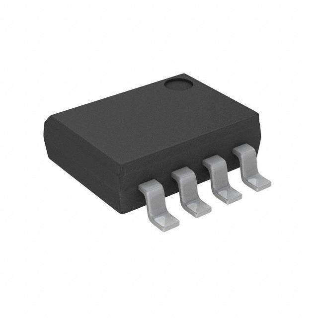
11LC010T-I/MNY产品简介:
ICGOO电子元器件商城为您提供11LC010T-I/MNY由Microchip设计生产,在icgoo商城现货销售,并且可以通过原厂、代理商等渠道进行代购。 11LC010T-I/MNY价格参考。Microchip11LC010T-I/MNY封装/规格:存储器, EEPROM 存储器 IC 1Kb (128 x 8) 单线 100kHz 8-TDFN(2x3)。您可以下载11LC010T-I/MNY参考资料、Datasheet数据手册功能说明书,资料中有11LC010T-I/MNY 详细功能的应用电路图电压和使用方法及教程。
Microchip Technology的11LC010T-I/MNY是一款1K x 8位(即1Kbit)的串行EEPROM存储器,采用I²C通信接口,工作电压范围为1.8V至5.5V,封装形式为SOT-23-6,具有体积小、功耗低、可靠性高的特点。

该器件广泛应用于对空间和功耗要求较高的嵌入式系统中。典型应用场景包括:消费类电子产品(如智能手机、平板电脑、可穿戴设备)中用于存储配置参数或校准数据;工业控制设备中保存运行设置、设备标识或故障日志;通信模块中存储MAC地址、序列号等唯一识别信息;医疗设备中记录使用数据或校准信息以确保精度;汽车电子中的传感器模块或车载附件,用于保存配置和状态信息。

由于其宽电压工作范围和高抗干扰能力,11LC010T-I/MNY也适用于电池供电或环境复杂的场合。此外,支持I²C总线多设备挂接,便于系统扩展。其高耐久性(通常支持100万次擦写)和长达200年的数据保持能力,确保了长期稳定运行,适合需要频繁写入或长期数据存储的应用场景。
| 参数 | 数值 |
| 产品目录 | 集成电路 (IC)半导体 |
| 描述 | IC EEPROM 1KBIT 100KHZ 8TDFN电可擦除可编程只读存储器 1K 128 X 8 2.5V SERIAL EE IND |
| 产品分类 | |
| 品牌 | Microchip Technology |
| 产品手册 | |
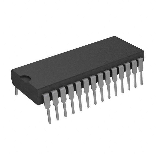
| 产品图片 |
|
| rohs | 符合RoHS无铅 / 符合限制有害物质指令(RoHS)规范要求 |
| 产品系列 | 内存,电可擦除可编程只读存储器,Microchip Technology 11LC010T-I/MNY- |
| 数据手册 | http://www.microchip.com/mymicrochip/filehandler.aspx?ddocname=en535318点击此处下载产品Datasheethttp://www.microchip.com/mymicrochip/filehandler.aspx?ddocname=en535315 |
| 产品型号 | 11LC010T-I/MNY |
| 产品目录页面 | |
| 产品种类 | 电可擦除可编程只读存储器 |
| 供应商器件封装 | 8-TDFN(2x3) |
| 其它名称 | 11LC010T-I/MNYCT |
| 包装 | 剪切带 (CT) |
| 商标 | Microchip Technology |
| 存储器类型 | EEPROM |
| 存储容量 | 1K (128 x 8) |
| 安装风格 | SMD/SMT |
| 封装 | Reel |
| 封装/外壳 | 8-WFDFN 裸露焊盘 |
| 封装/箱体 | TDFN-8 |
| 工作温度 | -40°C ~ 85°C |
| 工作电流 | 5 mA |
| 工作电源电压 | 3.3 V, 5 V |
| 工厂包装数量 | 3300 |
| 接口 | UNI/O™(单线) |
| 接口类型 | Serial |
| 数据保留 | 200 yr |
| 最大工作温度 | + 85 C |
| 最大工作电流 | 50 uA |
| 最大时钟频率 | 100 kHz |
| 最小工作温度 | - 40 C |
| 标准包装 | 1 |
| 格式-存储器 | EEPROMs - 串行 |
| 电压-电源 | 2.5 V ~ 5.5 V |
| 电源电压-最大 | 5.5 V |
| 电源电压-最小 | 2.5 V |
| 组织 | 128 x 8 |
| 速度 | 100kHz |


_renders/IS66WVE4M16EBLL-70BLI.jpg)

PDF Datasheet 数据手册内容提取
11AA010/11LC010 11AA080/11LC080 11AA020/11LC020 11AA160/11LC160 11AA040/11LC040 11AA161/11LC161 1K-16K UNI/O® Serial EEPROM Family Data Sheet Features: Description: • Single I/O, UNI/O® Serial Interface Bus The Microchip Technology Inc. 11AAXXX/11LCXXX • Low-Power CMOS Technology: (11XX*) devices are a family of 1 Kbit through 16 Kbit Serial Electrically Erasable PROMs. The devices are - 1mA active current, typical organized in blocks of x8-bit memory and support the - 1µA standby current (max.) (I-temp) patented** single I/O UNI/O® serial bus. By using • 128 x 8 through 2,048 x 8 Bit Organizations Manchester encoding techniques, the clock and data • Schmitt Trigger Inputs for Noise Suppression are combined into a single, serial bit stream (SCIO), • Output Slope Control to Eliminate Ground Bounce where the clock signal is extracted by the receiver to • 100 kbps Max. Bit Rate – Equivalent to 100 kHz correctly decode the timing and value of each bit. Clock Frequency Low-voltage design permits operation down to 1.8V (for • Self-Timed Write Cycle (including Auto-Erase) 11AAXXX devices), with standby and active currents of • Page-Write Buffer for up to 16 Bytes only 1 uA and 1 mA, respectively. • STATUS Register for Added Control: The 11XX family is available in standard packages - Write enable latch bit including 8-lead PDIP and SOIC, and advanced pack- aging including 3-lead SOT-23, 3-lead TO-92, 4-lead - Write-In-Progress bit Chip Scale, 8-lead TDFN, and 8-lead MSOP. • Block Write Protection: - Protect none, 1/4, 1/2 or all of array Package Types (not to scale) • Built-in Write Protection: - Power-on/off data protection circuitry MSOP PDIP/SOIC (MS) (P, SN) - Write enable latch • High Reliability: NC 1 8 VCC NC 1 8 VCC - Endurance: 1,000,000 erase/write cycles NC 2 7 NC NC 2 7 NC NC 3 6 NC - Data retention: > 200 years VSS 4 5 SCIO NC 3 6 NC Vss 4 5 SCIO - ESD protection: > 4,000V • 3-lead SOT-23 and TO-92 Packages TDFN SOT23 • 4-lead Chip Scale Package (MN) (TT) • 8-lead PDIP, SOIC, MSOP, TDFN Packages NC 1 8 VCC 2 VCC • Pb-Free and RoHS Compliant NC 2 7 NC VSS 3 • Available Temperature Ranges: NC 3 6 NC 1 SCIO - Industrial (I): -40°C to +85°C VSS 4 5 SCIO - Automotive (E): -40°C to +125°C CS (Chip Scale)(1) Pin Function Table TO-92 (TO) VCC 1 2 VSS Name Function SCIO Serial Clock, Data Input/Output SCIO 3 4 NC VSS Ground Vss (Top down view, VCC Supply Voltage Vcc SCIO balls not visible) Note 1: Available in I-temp, “AA” only. * 11XX is used in this document as a generic part number for the 11 series devices. ** Microchip’s UNI/O® Bus products are covered by some or all of the following patents issued in the U.S.A.: 7,376,020 & 7,788,430. 2011 Microchip Technology Inc. DS22067J-page 1
11XX DEVICE SELECTION TABLE Density Page Size Temp. Device Part Number Organization VCC Range Packages (bits) (Bytes) Ranges Address 11LC010 1K 128 x 8 2.5-5.5V 16 I,E 0xA0 P, SN, MS, MN, TO, TT 11AA010 1K 128 x 8 1.8-5.5V 16 I 0xA0 P, SN, MS, MN, TO, TT, CS 11LC020 2K 256 x 8 2.5-5.5V 16 I,E 0xA0 P, SN, MS, MN, TO, TT 11AA020 2K 256 x 8 1.8-5.5V 16 I 0xA0 P, SN, MS, MN, TO, TT, CS 11LC040 4K 512 x 8 2.5-5.5V 16 I,E 0xA0 P, SN, MS, MN, TO, TT 11AA040 4K 512 x 8 1.8-5.5V 16 I 0xA0 P, SN, MS, MN, TO, TT, CS 11LC080 8K 1,024 x 8 2.5-5.5V 16 I,E 0xA0 P, SN, MS, MN, TO, TT 11AA080 8K 1,024 x 8 1.8-5.5V 16 I 0xA0 P, SN, MS, MN, TO, TT, CS 11LC160 16K 2,048 x 8 2.5-5.5V 16 I,E 0xA0 P, SN, MS, MN, TO, TT 11AA160 16K 2,048 x 8 1.8-5.5V 16 I 0xA0 P, SN, MS, MN, TO, TT,CS 11LC161 16K 2,048 x 8 2.5-5.5V 16 I, E 0xA1 P, SN, MS, MN, TO, TT 11AA161 16K 2,048 x 8 1.8-5.5V 16 I 0xA1 P, SN, MS, MN, TO, TT, CS DS22067J-page 2 2011 Microchip Technology Inc.
11XX 1.0 ELECTRICAL CHARACTERISTICS Absolute Maximum Ratings (†) VCC.............................................................................................................................................................................6.5V SCIO w.r.t. VSS.....................................................................................................................................-0.6V to VCC+1.0V Storage temperature.................................................................................................................................-65°C to 150°C Ambient temperature under bias...............................................................................................................-40°C to 125°C ESD protection on all pins..........................................................................................................................................4kV † NOTICE: Stresses above those listed under ‘Absolute Maximum Ratings’ may cause permanent damage to the device. This is a stress rating only and functional operation of the device at those or any other conditions above those indicated in the operational listings of this specification is not implied. Exposure to maximum rating conditions for an extended period of time may affect device reliability. TABLE 1-1: DC CHARACTERISTICS Electrical Characteristics: Industrial (I): VCC = 2.5V to 5.5V TA = -40°C to +85°C DC CHARACTERISTICS VCC = 1.8V to 2.5V TA = -20°C to +85°C Automotive (E): VCC = 2.5V to 5.5V TA = -40°C to +125°C Param. Sym. Characteristic Min. Max. Units Test Conditions No. D1 VIH High-level input 0.7*VCC VCC+1 V voltage D2 VIL Low-level input -0.3 0.3*VCC V VCC2.5V voltage -0.3 0.2*VCC V VCC < 2.5V D3 VHYS Hysteresis of Schmitt 0.05*Vcc — V VCC2.5V (Note1) Trigger inputs (SCIO) D4 VOH High-level output VCC -0.5 — V IOH = -300 A, VCC = 5.5V voltage VCC -0.5 — V IOH = -200 A, Vcc = 2.5V D5 VOL Low-level output — 0.4 V IOI = 300 A, VCC = 5.5V voltage — 0.4 V IOI = 200 A, Vcc = 2.5V D6 IO Output current limit — ±4 mA VCC = 5.5V (Note 1) (Note 2) — ±3 mA Vcc = 2.5V (Note 1) D7 ILI Input leakage current — ±1 A VIN = VSS or VCC (SCIO) D8 CINT Internal Capacitance — 7 pF TA = 25°C, FCLK = 1MHz, (all inputs and VCC = 5.0V (Note1) outputs) D9 ICC Read Read Operating — 3 mA VCC=5.5V; FBUS=100kHz, CB=100 pF Current — 1 mA VCC=2.5V; FBUS=100kHz, CB=100 pF D10 ICC Write Write Operating — 5 mA VCC = 5.5V Current — 3 mA VCC = 2.5V D11 Iccs Standby Current — 5 A VCC = 5.5V TA = 125°C — 1 A VCC = 5.5V TA = 85°C D12 ICCI Idle Mode Current — 50 A VCC = 5.5V Note 1: This parameter is periodically sampled and not 100% tested. 2: The SCIO output driver impedance will vary to ensure IO is not exceeded. 2011 Microchip Technology Inc. DS22067J-page 3
11XX TABLE 1-2: AC CHARACTERISTICS Electrical Characteristics: Industrial (I): VCC = 2.5V to 5.5V TA = -40°C to +85°C AC CHARACTERISTICS VCC = 1.8V to 2.5V TA = -20°C to +85°C Automotive (E): VCC = 2.5V to 5.5V TA = -40°C to +125°C Param. Sym. Characteristic Min. Max. Units Test Conditions No. 1 FBUS Serial bus frequency 10 100 kHz — 2 TE Bit period 10 100 µs — 3 TIJIT Input edge jitter tolerance — ±0.06 UI (Note 3) 4 FDRIFT Serial bus frequency drift — ±0.50 % per byte — rate tolerance 5 FDEV Serial bus frequency drift — ±5 % per — limit command 6 TOJIT Output edge jitter — ±0.25 UI (Note 3) 7 TR SCIO input rise time — 100 ns — (Note1) 8 TF SCIO input fall time — 100 ns — (Note1) 9 TSTBY Standby pulse time 600 — µs — 10 TSS Start header setup time 10 — µs — 11 THDR Start header low pulse 5 — µs — time 12 TSP Input filter spike — 50 ns (Note1) suppression (SCIO) 13 TWC Write cycle time — 5 ms Write, WRSR commands (byte or page) — 10 ms ERAL, SETAL commands 14 — Endurance (per page) 1M — cycles 25°C, VCC = 5.5V (Note2) Note 1: This parameter is periodically sampled and not 100% tested. 2: This parameter is not tested but ensured by characterization. For endurance estimates in a specific application, please consult the Total Endurance™ Model which can be obtained on Microchip’s web site: www.microchip.com. 3: A Unit Interval (UI) is equal to 1-bit period (TE) at the current bus frequency. TABLE 1-3: AC TEST CONDITIONS AC Waveform: VLO = 0.2V VHI = VCC - 0.2V CL = 100 pF Timing Measurement Reference Level Input 0.5 VCC Output 0.5 VCC DS22067J-page 4 2011 Microchip Technology Inc.
11XX FIGURE 1-1: BUS TIMING – START HEADER 10 11 2 SCIO Data ‘0’ Data ‘1’ Data ‘0’ Data ‘1’ Data ‘0’ Data ‘1’ Data ‘0’ Data ‘1’ MAK bit NoSAK bit FIGURE 1-2: BUS TIMING – DATA 2 7 8 12 SCIO Data ‘0’ Data ‘1’ Data ‘1’ Data ‘0’ FIGURE 1-3: BUS TIMING – STANDBY PULSE 9 SCIO Standby Mode FIGURE 1-4: BUS TIMING – JITTER 2 2 3 3 6 6 6 6 Ideal Edge Ideal Edge Ideal Edge Ideal Edge from Master from Master from Slave from Slave 2011 Microchip Technology Inc. DS22067J-page 5
11XX 2.0 FUNCTIONAL DESCRIPTION 2.1 Principles of Operation The 11XX family of serial EEPROMs support the UNI/O® protocol. They can be interfaced with microcontrollers, including Microchip’s PIC® microcon- trollers, ASICs, or any other device with an available discrete I/O line that can be configured properly to match the UNI/O protocol. The 11XX devices contain an 8-bit instruction register. The devices are accessed via the SCIO pin. Table4-1 contains a list of the possible instruction bytes and format for device operation. All instructions, addresses, and data are transferred MSb first, LSb last. Data is embedded into the I/O stream through Manchester encoding. The bus is controlled by a master device which determines the clock period, con- trols the bus access and initiates all operations, while the 11XX works as slave. Both master and slave can operate as transmitter or receiver, but the master device determines which mode is active. FIGURE 2-1: BLOCK DIAGRAM STATUS HV Generator Register EEPROM I/O Control Memory X Control Array Logic Logic Dec Page Latches Current- Limited Slope Control Y Decoder SCIO Sense Amp. Vcc R/W Control Vss DS22067J-page 6 2011 Microchip Technology Inc.
11XX 3.0 BUS CHARACTERISTICS If a command is terminated in any manner other than a NoMAK/SAK combination, then the master must per- 3.1 Standby Pulse form a standby pulse before beginning a new com- mand, regardless of which device is to be selected. When the master has control of SCIO, a standby pulse can be generated by holding SCIO high for TSTBY. At Note: After a POR/BOR event occurs, a low- this time, the 11XX will reset and return to Standby to-high transition on SCIO must be gen- mode. Subsequently, a high-to-low transition on SCIO erated before proceeding with commu- (the first low pulse of the header) will return the device nication, including a standby pulse. to the active state. An example of two consecutive commands is shown in Once a command is terminated satisfactorily (i.e., via Figure3-1. Note that the device address is the same a NoMAK/SAK combination during the Acknowledge for both commands, indicating that the same device is being selected both times. sequence), performing a standby pulse is not required to begin a new command as long as the device to be A standby pulse cannot be generated while the slave selected is the same device selected during the previ- has control of SCIO. In this situation, the master must ous command. However, a period of TSS must be wait for the slave to finish transmitting and to release observed after the end of the command and before the SCIO before the pulse can be generated. beginning of the start header. After TSS, the start If, at any point during a command, an error is detected header (including THDR low pulse) can be transmitted by the master, a standby pulse should be generated in order to begin the new command. and the command should be performed again. FIGURE 3-1: CONSECUTIVE COMMANDS EXAMPLE K A Standby Pulse(1) Start Header AK oS Device Address AK AK M N M S SCIO 0 1 0 1 0 1 0 1 1 0 1 0 0 0 0 0 K A K NoM SAK TSS Start Header MAK NoSA Device Address MAK SAK SCIO 0 1 0 1 0 1 0 1 1 0 1 0 0 0 0 0 Note1: After a POR/BOR event, a low-to-high transition on SCIO is required to occur before the first standby pulse. 3.2 Start Data Transfer When a standby pulse is not required (i.e., between successive commands to the same device), a period of All operations must be preceded by a start header. The TSS must be observed after the end of the command start header consists of holding SCIO low for a period and before the beginning of the start header. of THDR, followed by transmitting an 8-bit ‘01010101’ Figure3-2 shows the waveform for the start header, code. This code is used to synchronize the slave’s including the required Acknowledge sequence at the internal clock period with the master’s clock period, so end of the byte. accurate timing is very important. FIGURE 3-2: START HEADER SCIO TSS THDR Data ‘0’ Data ‘1’ Data ‘0’ Data ‘1’ Data ‘0’ Data ‘1’ Data ‘0’ Data ‘1’ MAK NoSAK 2011 Microchip Technology Inc. DS22067J-page 7
11XX 3.3 Acknowledge FIGURE 3-4: ACKNOWLEDGE BITS An Acknowledge routine occurs after each byte is MAK (‘1’) SAK (‘1’) transmitted, including the start header. This routine consists of two bits. The first bit is transmitted by the master, and the second bit is transmitted by the slave. Note: A MAK must always be transmitted NoMAK (‘0’) NoSAK(1) following the start header. The Master Acknowledge, or MAK, is signified by trans- mitting a ‘1’, and informs the slave that the current operation is to be continued. Conversely, a Not Acknowledge, or NoMAK, is signified by transmitting a Note 1: A NoSAK is defined as any sequence that is not a ‘0’, and is used to end the current operation (and initiate valid SAK. the write cycle for write operations). 3.4 Device Addressing Note: When a NoMAK is used to end a A device address byte is the first byte received from the WRITE or WRSR instruction, the write master device following the start header. The device cycle is not initiated if no bytes of data address byte consists of a four-bit family code, for the have been received. 11XX this is set as ‘1010’. The last four bits of the The slave Acknowledge, or SAK, is also signified by device address byte are the device code, which is transmitting a ‘1’, and confirms proper communication. hardwired to ‘0000’ on the 11XXXX0 devices. However, unlike the NoMAK, the NoSAK is signified by The device code on 11XXXX1 devices is hardwired to the lack of a middle edge during the bit period. ‘0001’. This allows both 11XXXX0 and 11XXXX1 Note: In order to guard against bus conten- devices to be used on the same bus without address tion, a NoSAK will occur after the start conflicts. header. A NoSAK will occur for the following events: FIGURE 3-5: DEVICE ADDRESS BYTE ALLOCATION • Following the start header • Following the device address, if no slave on the SLAVE ADDRESS MAKSAK bus matches the transmitted address • Following the command byte, if the command is invalid, including Read, CRRD, Write, WRSR, SETAL, and ERAL during a write cycle. 1 0 1 0 0 0 0 0(1) • If the slave becomes out of sync with the master • If a command is terminated prematurely by using Note 1: This bit is a ‘1’ on the 11XXXX1. a NoMAK, with the exception of immediately after the device address. 3.5 Bus Conflict Protection See Figure3.3 and Figure3-4 for details. To help guard against high current conditions arising If a NoSAK is received from the slave after any byte from bus conflicts, the 11XX features a current-limited (except the start header), an error has occurred. The output driver. The IOL and IOH specifications describe master should then perform a standby pulse and begin the maximum current that can be sunk or sourced, the desired command again. respectively, by the SCIO pin. The 11XX will vary the output driver impedance to ensure that the maximum FIGURE 3-3: ACKNOWLEDGE current level is not exceeded. ROUTINE Master Slave MAK SAK DS22067J-page 8 2011 Microchip Technology Inc.
11XX 3.6 Device Standby 3.8.1 FREQUENCY DRIFT The 11XX features a low-power Standby mode during Within a system, there is a possibility that frequencies which the device is waiting to begin a new command. can drift due to changes in voltage, temperature, etc. A high-to-low transition on SCIO will exit low-power The re-synchronization circuitry provides some toler- mode and prepare the device for receiving the start ance for such frequency drift. The tolerance range is header. specified by two parameters, FDRIFT and FDEV. FDRIFT specifies the maximum tolerable change in bus fre- Standby mode will be entered upon the following quency per byte. FDEV specifies the overall limit in fre- conditions: quency deviation within an operation (i.e., from the end • A NoMAK followed by a SAK (i.e., valid termina- of the start header until communication is terminated tion of a command) for that operation). The start header at the beginning of • Reception of a standby pulse the next operation will reset the re-synchronization cir- cuitry and allow for another FDEV amount of frequency Note: In the case of the WRITE, WRSR, SETAL, drift. or ERAL commands, the write cycle is initi- ated upon receipt of the NoMAK, assuming 3.8.2 EDGE JITTER all other write requirements have been met. Ensuring that edge transitions from the master always occur exactly in the middle or end of the bit period is not 3.7 Device Idle always possible. Therefore, the re-synchronization cir- The 11XX features an Idle mode during which all serial cuitry is designed to provide some tolerance for edge data is ignored until a standby pulse occurs. Idle mode jitter. will be entered upon the following conditions: The 11XX adjusts its phase every MAK bit, so TIJIT • Invalid device address specifies the maximum allowable peak-to-peak jitter relative to the previous MAK bit. Since the position of • Invalid command byte, including Read, CRRD, Write, WRSR, SETAL and ERAL during a write the previous MAK bit would be difficult to measure by the master, the minimum and maximum jitter values for cycle. a system should be considered the worst-case. These • Missed edge transition values will be based on the execution time for different • Reception of a MAK following a WREN, WRDI, branch paths in software, jitter due to thermal noise, SETAL, or ERAL command byte etc. • Reception of a MAK following the data byte of a The difference between the minimum and maximum WRSR command values, as a percentage of the bit period, should be cal- An invalid start header will indirectly cause the device culated and then compared against TIJIT to determine to enter Idle mode. Whether or not the start header is jitter compliance. invalid cannot be detected by the slave, but will prevent the slave from synchronizing properly with the master. If the slave is not synchronized with the Note: Because the 11XX only re-synchronizes master, an edge transition will be missed, thus causing during the MAK bit, the overall ability to the device to enter Idle mode. remain synchronized depends on a combi- nation of frequency drift and edge jitter (i.e., 3.8 Synchronization if the MAK bit edge is experiencing the max- imum allowable edge jitter, then there is no At the beginning of every command, the 11XX utilizes room for frequency drift). Conversely, if the the start header to determine the master’s bus clock frequency has drifted to the maximum period. This period is then used as a reference for all amount tolerable within a byte, then no subsequent communication within that command. edge jitter can be present. The 11XX features re-synchronization circuitry which will monitor the position of the middle data edge during each MAK bit and subsequently adjust the internal time reference in order to remain synchronized with the master. There are two variables which can cause the 11XX to lose synchronization. The first is frequency drift, defined as a change in the bit period, TE. The second is edge jitter, which is a single occurrence change in the position of an edge within a bit period, while the bit period itself remains constant. 2011 Microchip Technology Inc. DS22067J-page 9
11XX 4.0 DEVICE COMMANDS After the device address byte, a command byte must be sent by the master to indicate the type of operation to be performed. The code for each instruction is listed in Table4-1. TABLE 4-1: INSTRUCTION SET Instruction Name Instruction Code Hex Code Description READ 0000 0011 0x03 Read data from memory array beginning at specified address CRRD 0000 0110 0x06 Read data from current location in memory array WRITE 0110 1100 0x6C Write data to memory array beginning at specified address WREN 1001 0110 0x96 Set the write enable latch (enable write operations) WRDI 1001 0001 0x91 Reset the write enable latch (disable write operations) RDSR 0000 0101 0x05 Read STATUS register WRSR 0110 1110 0x6E Write STATUS register ERAL 0110 1101 0x6D Write ‘0x00’ to entire array SETAL 0110 0111 0x67 Write ‘0xFF’ to entire array 4.1 Read Instruction that the slave should output the next data byte. This continues until the master sends a NoMAK, which ends The Read command allows the master to access any the operation. memory location in a random manner. After the READ To provide sequential reads in this manner, the 11XX instruction has been sent to the slave, the two bytes of contains an internal Address Pointer which is incre- the Word Address are transmitted, with an Acknowl- mented by one after the transmission of each byte. This edge sequence being performed after each byte. Then, Address Pointer allows the entire memory contents to the slave sends the first data byte to the master. If more be serially read during one operation. When the highest data is to be read, the master sends a MAK, indicating address is reached, the Address Pointer rolls over to address ‘0x000’ if the master chooses to continue the operation by providing a MAK. FIGURE 4-1: READ COMMAND SEQUENCE K A K S K K Standby Pulse Start Header A o Device Address A A M N M S SCIO 0 1 0 1 0 1 0 1 1 0 1 0 0 0 0 0(1) K K K K K K Command A A Word Address MSB A A Word Address LSB A A M S M S M S SCIO 1514131211 10 9 8 7 6 5 4 3 2 1 0 0 0 0 0 0 0 1 1 K A K K K K M K Data Byte 1 A A Data Byte 2 A A Data Byte n o A M S M S N S SCIO 7 6 5 4 3 2 1 0 7 6 5 4 3 2 1 0 7 6 5 4 3 2 1 0 Note1: For the 11XXXX1, this bit must be a ‘1’. DS22067J-page 10 2011 Microchip Technology Inc.
11XX 4.2 Current Address Read (CRRD) TABLE 4-2: INTERNAL ADDRESS Instruction COUNTER The internal address counter featured on the 11XX Command Event Action maintains the address of the last memory array loca- — Power-on Reset Counter is undefined tion accessed. The CRRD instruction allows the mas- READ or MAK edge fol- Counter is updated ter to read data back beginning from this current WRITE lowing each with newly received location. Consequently, no word address is provided Address byte value upon issuing this command. READ, MAK/NoMAK Counter is incre- Note that, except for the initial word address, the WRITE, or edge following mented by 1 READ and CRRD instructions are identical, including CRRD each data byte the ability to continue requesting data through the use of MAKs in order to sequentially read from the array. Note: If, following each data byte in a READ, As with the READ instruction, the CRRD instruction is WRITE, or CRRD instruction, neither a terminated by transmitting a NoMAK. MAK nor a NoMAK edge is received Table4-2 lists the events upon which the internal (i.e., if a standby pulse occurs instead), address counter is modified. the internal address counter will not be incremented. Note: During a Write command, once the last data byte for a page has been loaded, the internal Address Pointer will rollover to the beginning of the selected page. FIGURE 4-2: CRRD COMMAND SEQUENCE K A K S K K Standby Pulse Start Header A o Device Address A A M N M S SCIO 0 1 0 1 0 1 0 1 1 0 1 0 0 0 0 0(1) K K K K K K Command A A Data Byte 1 A A Data Byte 2 A A M S M S M S SCIO 7 6 5 4 3 2 1 0 7 6 5 4 3 2 1 0 0 0 0 0 0 1 1 0 K A M K Data Byte n o A N S SCIO 7 6 5 4 3 2 1 0 Note1: For the 11XXXX1, this bit must be a ‘1’. 2011 Microchip Technology Inc. DS22067J-page 11
11XX 4.3 Write Instruction Upon receipt of each word, the four lower-order Address Pointer bits are internally incremented by one. Prior to any attempt to write data to the 11XX, the write The higher-order bits of the word address remain con- enable latch must be set by issuing the WREN stant. If the master should transmit data past the end of instruction (see Section4.4 “Write Enable (WREN) the page, the address counter will roll over to the begin- and Write Disable (WRDI) Instructions”). ning of the page, where further received data will be Once the write enable latch is set, the user may pro- written. ceed with issuing a WRITE instruction (including the Note: Page write operations are limited to writ- header and device address bytes) followed by the MSB ing bytes within a single physical page, and LSB of the Word Address. Once the last Acknowl- regardless of the number of bytes actu- edge sequence has been performed, the master ally being written. Physical page bound- transmits the data byte to be written. aries start at addresses that are integer The 11XX features a 16-byte page buffer, meaning that multiples of the page size (16 bytes) and up to 16 bytes can be written at one time. To utilize this end at addresses that are integer multi- feature, the master can transmit up to 16 data bytes to ples of the page size minus 1. As an the 11XX, which are temporarily stored in the page buf- example, the page that begins at fer. After each data byte, the master sends a MAK, indi- address 0x30 ends at address 0x3F. If a cating whether or not another data byte is to follow. A page Write command attempts to write NoMAK indicates that no more data is to follow, and as across a physical page boundary, the such will initiate the internal write cycle. result is that the data wraps around to the beginning of the current page (over- Note: If a NoMAK is generated before any writing data previously stored there), data has been provided, or if a standby instead of being written to the next page pulse occurs before the NoMAK is gen- as might be expected. It is therefore erated, the 11XX will be reset, and the necessary for the application software write cycle will not be initiated. to prevent page write operations that would attempt to cross a page bound- ary. FIGURE 4-3: WRITE COMMAND SEQUENCE K A K S K K Standby Pulse Start Header A o Device Address A A M N M S SCIO 0 1 0 1 0 1 0 1 1 0 1 0 0 0 0 0(1) K K K K K K Command A A Word Address MSB A A Word Address LSB A A M S M S M S SCIO 1514131211 10 9 8 7 6 5 4 3 2 1 0 0 1 1 0 1 1 0 0 K A M K K K K K Data Byte 1 A A Data Byte 2 A A Data Byte n o A M S M S N S SCIO 7 6 5 4 3 2 1 0 7 6 5 4 3 2 1 0 7 6 5 4 3 2 1 0 Twc Note1: For the 11XXXX1, this bit must be a ‘1’. DS22067J-page 12 2011 Microchip Technology Inc.
11XX 4.4 Write Enable (WREN) and Write The following is a list of conditions under which the Disable (WRDI) Instructions write enable latch will be reset: • Power-up The 11XX contains a write enable latch. See Table6-1 • WRDI instruction successfully executed for the Write-Protect Functionality Matrix. This latch must be set before any write operation will be com- • WRSR instruction successfully executed pleted internally. The WREN instruction will set the • WRITE instruction successfully executed latch, and the WRDI instruction will reset the latch. • ERAL instruction successfully executed Note: The WREN and WRDI instructions must • SETAL instruction successfully executed be terminated with a NoMAK following the command byte. If a NoMAK is not received at this point, the command will be considered invalid, and the device will go into Idle mode without respond- ing with a SAK or executing the com- mand. FIGURE 4-4: WRITE ENABLE COMMAND SEQUENCE K A K S K K Standby Pulse Start Header A o Device Address A A M N M S SCIO 0 1 0 1 0 1 0 1 1 0 1 0 0 0 0 0(1) K A M K Command o A N S SCIO 1 0 0 1 0 1 1 0 Note1: For the 11XXXX1, this bit must be a ‘1’. FIGURE 4-5: WRITE DISABLE COMMAND SEQUENCE K A K S K K Standby Pulse Start Header A o Device Address A A M N M S SCIO 0 1 0 1 0 1 0 1 1 0 1 0 0 0 0 0(1) K A M K Command o A N S SCIO 1 0 0 1 0 0 0 1 Note1: For the 11XXXX1, this bit must be a ‘1’. 2011 Microchip Technology Inc. DS22067J-page 13
11XX 4.5 Read Status Register (RDSR) The Block Protection (BP0 and BP1) bits indicate Instruction which blocks are currently write-protected. These bits are set by the user through the WRSR instruction. The RDSR instruction provides access to the STATUS These bits are nonvolatile. register. The STATUS register may be read at any time, Note: If Read Status Register command is even during a write cycle. The STATUS register is initiated while the 11XX is currently formatted as follows: executing an internal write cycle on the 7 6 5 4 3 2 1 0 STATUS register, the new Block X X X X BP1 BP0 WEL WIP Protection bit values will be read during Note: Bits 4-7 are don’t cares, and will read as ‘0’. the entire command. The Write-In-Process (WIP) bit indicates whether the The WIP and WEL bits will update dynamically (asyn- 11XX is busy with a write operation. When set to a ‘1’, chronous to issuing the RDSR instruction). Further- a write is in progress, when set to a ‘0’, no write is in more, after the STATUS register data is received, the progress. This bit is read-only. master can provide a MAK during the Acknowledge sequence to request that the data be transmitted again. The Write Enable Latch (WEL) bit indicates the status This allows the master to continuously monitor the WIP of the write enable latch. When set to a ‘1’, the latch and WEL bits without the need to issue another full allows writes to the array, when set to a ‘0’, the latch command. prohibits writes to the array. This bit is set and cleared using the WREN and WRDI instructions, respectively. Once the master is finished, it provides a NoMAK to This bit is read-only for any other instruction. end the operation. Note: The current drawn for a Read Status Register command during a write cycle is a combination of the ICC Read and ICC Write operating currents. FIGURE 4-6: READ STATUS REGISTER COMMAND SEQUENCE K A K S K K Standby Pulse Start Header A o Device Address A A M N M S SCIO 0 1 0 1 0 1 0 1 1 0 1 0 0 0 0 0(1) K A K K M K Command A A STATUS Register Data o A M S N S SCIO 3 2 1 0 0 0 0 0 0 1 0 1 0 0 0 0 Note1: For the 11XXXX1, this bit must be a ‘1’. Note 2:The STATUS register data can continuously be read, or polled, by transmitting a MAK in place of the NoMAK. DS22067J-page 14 2011 Microchip Technology Inc.
11XX 4.6 Write Status Register (WRSR) After transmitting the STATUS register data, the master Instruction must transmit a NoMAK during the Acknowledge sequence in order to initiate the internal write cycle. The WRSR instruction allows the user to select one of Note: The WRSR instruction must be termi- four levels of protection for the array by writing to the nated with a NoMAK following the data appropriate bits in the STATUS register. The array is byte. If a NoMAK is not received at this divided up into four segments. The user has the ability point, the command will be considered to write-protect none, one, two, or all four of the seg- invalid, and the device will go into Idle ments of the array. The partitioning is controlled as mode without responding with a SAK or illustrated in Table4-3. executing the command. TABLE 4-3: ARRAY PROTECTION BP1 BP0 Address Ranges Write-Protected Address Ranges Unprotected 0 0 None All 0 1 Upper 1/4 Lower 3/4 1 0 Upper 1/2 Lower 1/2 1 1 All None TABLE 4-4: PROTECTED ARRAY ADDRESS LOCATIONS Density Upper 1/4 Upper 1/2 All Sectors 1K 60h-7Fh 40h-7Fh 00h-7Fh 2K C0h-FFh 80h-FFh 00h-FFh 4K 180h-1FFh 100h-1FFh 000h-1FFh 8K 300h-3FFh 200h-3FFh 000h-3FFh 16K 600h-7FFh 400h-7FFh 000h-7FFh FIGURE 4-7: WRITE STATUS REGISTER COMMAND SEQUENCE K A K S K K Standby Pulse Start Header A o Device Address A A M N M S SCIO 0 1 0 1 0 1 0 1 1 0 1 0 0 0 0 0(1) K A K K M K Command A A Status Register Data o A M S N S SCIO 7 6 5 4 3 2 1 0 0 1 1 0 1 1 1 0 Twc Note1: For the 11XXXX1, this bit must be a ‘1’. 2011 Microchip Technology Inc. DS22067J-page 15
11XX 4.7 Erase All (ERAL) Instruction The ERAL instruction is ignored if either of the Block Protect bits (BP0, BP1) are not 0, meaning 1/4, 1/2, or The ERAL instruction allows the user to write ‘0x00’ to all of the array is protected. the entire memory array with one command. Note that the write enable latch (WEL) must first be set by issuing Note: The ERAL instruction must be termi- the WREN instruction. nated with a NoMAK following the com- mand byte. If a NoMAK is not received Once the write enable latch is set, the user may pro- at this point, the command will be con- ceed with issuing a ERAL instruction (including the sidered invalid, and the device will go header and device address bytes). Immediately after into Idle mode without responding with a the NoMAK bit has been transmitted by the master, the SAK or executing the command. internal write cycle is initiated, during which time all words of the memory array are written to ‘0x00’. FIGURE 4-8: ERASE ALL COMMAND SEQUENCE K A K S K K Standby Pulse Start Header A o Device Address A A M N M S SCIO 0 1 0 1 0 1 0 1 1 0 1 0 0 0 0 0(1) K A M K Command o A N S SCIO 0 1 1 0 1 1 0 1 Twc Note1: For the 11XXXX1, this bit must be a ‘1’. 4.8 Set All (SETAL) Instruction The SETAL instruction is ignored if either of the Block Protect bits (BP0, BP1) are not 0, meaning 1/4, 1/2, or The SETAL instruction allows the user to write ‘0xFF’ all of the array is protected. to the entire memory array with one command. Note that the write enable latch (WEL) must first be set by Note: The SETAL instruction must be termi- issuing the WREN instruction. nated with a NoMAK following the com- mand byte. If a NoMAK is not received Once the write enable latch is set, the user may pro- at this point, the command will be con- ceed with issuing a SETAL instruction (including the sidered invalid, and the device will go header and device address bytes). Immediately after into Idle mode without responding with a the NoMAK bit has been transmitted by the master, the SAK or executing the command. internal write cycle is initiated, during which time all words of the memory array are written to ‘0xFF’. FIGURE 4-9: SET ALL COMMAND SEQUENCE K A K S K K Standby Pulse Start Header A o Device Address A A M N M S SCIO 0 1 0 1 0 1 0 1 1 0 1 0 0 0 0 0(1) K A M K Command o A N S SCIO 0 1 1 0 0 1 1 1 Twc Note1: For the 11XXXX1, this bit must be a ‘1’. DS22067J-page 16 2011 Microchip Technology Inc.
11XX 5.0 DATA PROTECTION 6.0 POWER-ON STATE The following protection has been implemented to The 11XX powers on in the following state: prevent inadvertent writes to the array: • The device is in low-power Shutdown mode, • The Write Enable Latch (WEL) is reset on power- requiring a low-to-high transition on SCIO to enter up Idle mode • A Write Enable (WREN) instruction must be issued • The Write Enable Latch (WEL) is reset to set the write enable latch • The internal Address Pointer is undefined • After a write, ERAL, SETAL, or WRSR command, • A low-to-high transition, standby pulse and subse- the write enable latch is reset quent high-to-low transition on SCIO (the first low • Commands to access the array or write to the pulse of the header) are required to enter the status register are ignored during an internal write active state cycle and programming is not affected . TABLE 6-1: WRITE PROTECT FUNCTIONALITY MATRIX WEL Protected Blocks Unprotected Blocks Status Register 0 Protected Protected Protected 1 Protected Writable Writable 2011 Microchip Technology Inc. DS22067J-page 17
11XX 7.0 PIN DESCRIPTIONS The descriptions of the pins are listed in Table7-1. TABLE 7-1: PIN FUNCTION TABLE 8-pin PDIP/SOIC/ Name 3-pin SOT-23 3-pin TO-92 4-pin CS Description MSOP/TDFN SCIO 1 2 3 5 Serial Clock, Data Input/Output VCC 2 3 1 8 Supply Voltage VSS 3 1 2 4 Ground NC — — 4 1,2,3,6,7 No Internal Connection 7.1 Serial Clock, Data Input/Output (SCIO) SCIO is a bidirectional pin used to transfer commands and addresses into, as well as data into and out of, the device. The serial clock is embedded into the data stream through Manchester encoding. Each bit is represented by a signal transition at the middle of the bit period. DS22067J-page 18 2011 Microchip Technology Inc.
11XX 8.0 PACKAGING INFORMATION 8.1 Package Marking Information 8-Lead PDIP Example: XXXXXXXX 11AA160 T/XXXNNN I/P e 3 1L7 YYWW 0828 8-Lead PDIP Package Marking (Pb-Free) Device Line 1 Marking Device Line 1 Marking 11AA010 11AA010 11LC010 11LC010 11AA020 11AA020 11LC020 11LC020 11AA040 11AA040 11LC040 11LC040 11AA080 11AA080 11LC080 11LC080 11AA160 11AA160 11LC160 11LC160 11AA161 11AA161 11LC161 11LC161 Note: T = Temperature Grade (I, E) Legend: XX...X Customer-specific information Y Year code (last digit of calendar year) YY Year code (last 2 digits of calendar year) WW Week code (week of January 1 is week ‘01’) NNN Alphanumeric traceability code e3 Pb-free JEDEC designator for Matte Tin (Sn) * This package is Pb-free. The Pb-free JEDEC designator ( e 3 ) can be found on the outer packaging for this package. Note: In the event the full Microchip part number cannot be marked on one line, it will be carried over to the next line, thus limiting the number of available characters for customer-specific information. 2011 Microchip Technology Inc. DS22067J-page 19
11XX 8-Lead SOIC Example: XXXXXXXT 11AA160I XXXXYYWW SN e 3 0828 NNN 1L7 8-Lead SOIC Package Marking (Pb-Free) Device Line 1 Marking Device Line 1 Marking 11AA010 11AA010T 11LC010 11LC010T 11AA020 11AA020T 11LC020 11LC020T 11AA040 11AA040T 11LC040 11LC040T 11AA080 11AA080T 11LC080 11LC080T 11AA160 11AA160T 11LC160 11LC160T 11AA161 11AA161T 11LC161 11LC161T Note: T = Temperature Grade (I, E) Legend: XX...X Customer-specific information Y Year code (last digit of calendar year) YY Year code (last 2 digits of calendar year) WW Week code (week of January 1 is week ‘01’) NNN Alphanumeric traceability code e3 Pb-free JEDEC designator for Matte Tin (Sn) * This package is Pb-free. The Pb-free JEDEC designator ( e 3 ) can be found on the outer packaging for this package. Note: In the event the full Microchip part number cannot be marked on one line, it will be carried over to the next line, thus limiting the number of available characters for customer-specific information. DS22067J-page 20 2011 Microchip Technology Inc.
11XX 8-Lead MSOP (150 mil) Example: XXXXXXT 1e13A01I YWWNNN 8281L7 8-Lead MSOP Package Marking (Pb-Free) Device Line 1 Marking Device Line 1 Marking 11AA010 11A01T 11LC010 11L01T 11AA020 11A02T 11LC020 11L02T 11AA040 11A04T 11LC040 11L04T 11AA080 11A08T 11LC080 11L08T 11AA160 11AAT 11LC160 11LAT 11AA161 11AA1T 11LC161 11LA1T Note: T = Temperature Grade (I, E) Legend: XX...X Customer-specific information Y Year code (last digit of calendar year) YY Year code (last 2 digits of calendar year) WW Week code (week of January 1 is week ‘01’) NNN Alphanumeric traceability code e3 Pb-free JEDEC designator for Matte Tin (Sn) * This package is Pb-free. The Pb-free JEDEC designator ( e 3 ) can be found on the outer packaging for this package. Note: In the event the full Microchip part number cannot be marked on one line, it will be carried over to the next line, thus limiting the number of available characters for customer-specific information. 2011 Microchip Technology Inc. DS22067J-page 21
11XX 8-Lead 2x3 TDFN Example: XXX D51 YWW 828 NN 17 8-Lead 2x3 TDFN Package Marking (Pb-Free) Device I-Temp Marking Device I-Temp Marking E-Temp Marking 11AA010 D11 11LC010 D14 D15 11AA020 D21 11LC020 D24 D25 11AA040 D31 11LC040 D34 D35 11AA080 D41 11LC080 D44 D45 11AA160 D51 11LC160 D54 D55 11AA161 D5D 11LC161 D5G D5H Legend: XX...X Customer-specific information Y Year code (last digit of calendar year) YY Year code (last 2 digits of calendar year) WW Week code (week of January 1 is week ‘01’) NN Alphanumeric traceability code e3 Pb-free JEDEC designator for Matte Tin (Sn) * This package is Pb-free. The Pb-free JEDEC designator ( e 3 ) can be found on the outer packaging for this package. Note: In the event the full Microchip part number cannot be marked on one line, it will be carried over to the next line, thus limiting the number of available characters for customer-specific information. DS22067J-page 22 2011 Microchip Technology Inc.
11XX 3-Lead SOT-23 Example: XXNN B517 3-Lead SOT-23 Package Marking (Pb-Free) Device I-Temp Marking Device I-Temp Marking E-Temp Marking 11AA010 B1NN 11LC010 M1NN N1NN 11AA020 B2NN 11LC020 M2NN N2NN 11AA040 B3NN 11LC040 M3NN N3NN 11AA080 B4NN 11LC080 M4NN N4NN 11AA160 B5NN 11LC160 M5NN N5NN 11AA161 B0NN 11LC161 M0NN N0NN Legend: XX...X Customer-specific information Y Year code (last digit of calendar year) YY Year code (last 2 digits of calendar year) WW Week code (week of January 1 is week ‘01’) NNN Alphanumeric traceability code e3 Pb-free JEDEC designator for Matte Tin (Sn) * This package is Pb-free. The Pb-free JEDEC designator ( e 3 ) can be found on the outer packaging for this package. Note: In the event the full Microchip part number cannot be marked on one line, it will be carried over to the next line, thus limiting the number of available characters for customer-specific information. 2011 Microchip Technology Inc. DS22067J-page 23
11XX 3-Lead TO-92 Example: XXXXXX 11A160 T/XXXX I/TeO3 e3 YWW 928 NNN 1L7 3-Lead TO-92 Package Marking (Pb-Free) Device Line 1 Marking Device Line 1 Marking 11AA010 11A010 11LC010 11L010 11AA020 11A020 11LC020 11L020 11AA040 11A040 11LC040 11L040 11AA080 11A080 11LC080 11L080 11AA160 11A160 11LC160 11L160 11AA161 11A161 11LC161 11L161 Note: T = Temperature Grade (I, E) Legend: XX...X Customer-specific information Y Year code (last digit of calendar year) YY Year code (last 2 digits of calendar year) WW Week code (week of January 1 is week ‘01’) NNN Alphanumeric traceability code e3 Pb-free JEDEC designator for Matte Tin (Sn) * This package is Pb-free. The Pb-free JEDEC designator ( e 3 ) can be found on the outer packaging for this package. Note: In the event the full Microchip part number cannot be marked on one line, it will be carried over to the next line, thus limiting the number of available characters for customer-specific information. DS22067J-page 24 2011 Microchip Technology Inc.
11XX 4-Lead Chip Scale Example: XW E3 NN 17 4-Lead Chip Scale Package Marking (Pb-Free) Device Line 1 Marking 11AA010 AW 11AA020 BW 11AA040 CW 11AA080 DW 11AA160 EW 11AA161 HW Legend: XX...X Customer-specific information Y Year code (last digit of calendar year) YY Year code (last 2 digits of calendar year) WW Week code (week of January 1 is week ‘01’) NNN Alphanumeric traceability code e3 Pb-free JEDEC designator for Matte Tin (Sn) * This package is Pb-free. The Pb-free JEDEC designator ( e 3 ) can be found on the outer packaging for this package. Note: In the event the full Microchip part number cannot be marked on one line, it will be carried over to the next line, thus limiting the number of available characters for customer-specific information. 2011 Microchip Technology Inc. DS22067J-page 25
11XX (cid:2)(cid:3)(cid:4)(cid:5)(cid:6)(cid:7)(cid:8)(cid:9)(cid:10)(cid:6)(cid:11)(cid:12)(cid:13)(cid:14)(cid:8)(cid:15)(cid:16)(cid:6)(cid:10)(cid:8)(cid:17)(cid:18)(cid:3)(cid:4)(cid:13)(cid:18)(cid:5)(cid:8)(cid:19)(cid:9)(cid:20)(cid:8)(cid:21)(cid:8)(cid:22)(cid:23)(cid:23)(cid:8)(cid:24)(cid:13)(cid:10)(cid:8)(cid:25)(cid:26)(cid:7)(cid:27)(cid:8)(cid:28)(cid:9)(cid:15)(cid:17)(cid:9)(cid:29) (cid:30)(cid:26)(cid:12)(cid:5)(cid:31) 3(cid:10)(cid:9)(cid:2)&(cid:11)(cid:14)(cid:2)’(cid:10)!&(cid:2)(cid:8)"(cid:9)(cid:9)(cid:14)(cid:15)&(cid:2)(cid:12)(cid:28)(cid:8)4(cid:28)(cid:17)(cid:14)(cid:2)#(cid:9)(cid:28)*(cid:7)(cid:15)(cid:17)!((cid:2)(cid:12)(cid:16)(cid:14)(cid:28)!(cid:14)(cid:2)!(cid:14)(cid:14)(cid:2)&(cid:11)(cid:14)(cid:2)(cid:6)(cid:7)(cid:8)(cid:9)(cid:10)(cid:8)(cid:11)(cid:7)(cid:12)(cid:2)(cid:31)(cid:28)(cid:8)4(cid:28)(cid:17)(cid:7)(cid:15)(cid:17)(cid:2)(cid:22)(cid:12)(cid:14)(cid:8)(cid:7)%(cid:7)(cid:8)(cid:28)&(cid:7)(cid:10)(cid:15)(cid:2)(cid:16)(cid:10)(cid:8)(cid:28)&(cid:14)#(cid:2)(cid:28)&(cid:2) (cid:11)&&(cid:12)255***(cid:20)’(cid:7)(cid:8)(cid:9)(cid:10)(cid:8)(cid:11)(cid:7)(cid:12)(cid:20)(cid:8)(cid:10)’5(cid:12)(cid:28)(cid:8)4(cid:28)(cid:17)(cid:7)(cid:15)(cid:17) N NOTE1 E1 1 2 3 D E A A2 L A1 c e eB b1 b 6(cid:15)(cid:7)&! (cid:19)7,8.(cid:22) (cid:21)(cid:7)’(cid:14)(cid:15)!(cid:7)(cid:10)(cid:15)(cid:2)9(cid:7)’(cid:7)&! (cid:6)(cid:19)7 7:(cid:6) (cid:6)(cid:25); 7"’)(cid:14)(cid:9)(cid:2)(cid:10)%(cid:2)(cid:31)(cid:7)(cid:15)! 7 < (cid:31)(cid:7)&(cid:8)(cid:11) (cid:14) (cid:20)(cid:30)(cid:4)(cid:4)(cid:2)1(cid:22), (cid:13)(cid:10)(cid:12)(cid:2)&(cid:10)(cid:2)(cid:22)(cid:14)(cid:28)&(cid:7)(cid:15)(cid:17)(cid:2)(cid:31)(cid:16)(cid:28)(cid:15)(cid:14) (cid:25) = = (cid:20)(cid:3)(cid:30)(cid:4) (cid:6)(cid:10)(cid:16)#(cid:14)#(cid:2)(cid:31)(cid:28)(cid:8)4(cid:28)(cid:17)(cid:14)(cid:2)(cid:13)(cid:11)(cid:7)(cid:8)4(cid:15)(cid:14)!! (cid:25)(cid:3) (cid:20)(cid:30)(cid:30)(cid:29) (cid:20)(cid:30)-(cid:4) (cid:20)(cid:30)(cid:24)(cid:29) 1(cid:28)!(cid:14)(cid:2)&(cid:10)(cid:2)(cid:22)(cid:14)(cid:28)&(cid:7)(cid:15)(cid:17)(cid:2)(cid:31)(cid:16)(cid:28)(cid:15)(cid:14) (cid:25)(cid:30) (cid:20)(cid:4)(cid:30)(cid:29) = = (cid:22)(cid:11)(cid:10)"(cid:16)#(cid:14)(cid:9)(cid:2)&(cid:10)(cid:2)(cid:22)(cid:11)(cid:10)"(cid:16)#(cid:14)(cid:9)(cid:2)>(cid:7)#&(cid:11) . (cid:20)(cid:3)(cid:24)(cid:4) (cid:20)-(cid:30)(cid:4) (cid:20)-(cid:3)(cid:29) (cid:6)(cid:10)(cid:16)#(cid:14)#(cid:2)(cid:31)(cid:28)(cid:8)4(cid:28)(cid:17)(cid:14)(cid:2)>(cid:7)#&(cid:11) .(cid:30) (cid:20)(cid:3)(cid:23)(cid:4) (cid:20)(cid:3)(cid:29)(cid:4) (cid:20)(cid:3)<(cid:4) : (cid:14)(cid:9)(cid:28)(cid:16)(cid:16)(cid:2)9(cid:14)(cid:15)(cid:17)&(cid:11) (cid:21) (cid:20)-(cid:23)< (cid:20)-?(cid:29) (cid:20)(cid:23)(cid:4)(cid:4) (cid:13)(cid:7)(cid:12)(cid:2)&(cid:10)(cid:2)(cid:22)(cid:14)(cid:28)&(cid:7)(cid:15)(cid:17)(cid:2)(cid:31)(cid:16)(cid:28)(cid:15)(cid:14) 9 (cid:20)(cid:30)(cid:30)(cid:29) (cid:20)(cid:30)-(cid:4) (cid:20)(cid:30)(cid:29)(cid:4) 9(cid:14)(cid:28)#(cid:2)(cid:13)(cid:11)(cid:7)(cid:8)4(cid:15)(cid:14)!! (cid:8) (cid:20)(cid:4)(cid:4)< (cid:20)(cid:4)(cid:30)(cid:4) (cid:20)(cid:4)(cid:30)(cid:29) 6(cid:12)(cid:12)(cid:14)(cid:9)(cid:2)9(cid:14)(cid:28)#(cid:2)>(cid:7)#&(cid:11) )(cid:30) (cid:20)(cid:4)(cid:23)(cid:4) (cid:20)(cid:4)?(cid:4) (cid:20)(cid:4)(cid:5)(cid:4) 9(cid:10)*(cid:14)(cid:9)(cid:2)9(cid:14)(cid:28)#(cid:2)>(cid:7)#&(cid:11) ) (cid:20)(cid:4)(cid:30)(cid:23) (cid:20)(cid:4)(cid:30)< (cid:20)(cid:4)(cid:3)(cid:3) : (cid:14)(cid:9)(cid:28)(cid:16)(cid:16)(cid:2)(cid:26)(cid:10)*(cid:2)(cid:22)(cid:12)(cid:28)(cid:8)(cid:7)(cid:15)(cid:17)(cid:2)(cid:2)+ (cid:14)1 = = (cid:20)(cid:23)-(cid:4) (cid:30)(cid:26)(cid:12)(cid:5)(cid:11)(cid:31) (cid:30)(cid:20) (cid:31)(cid:7)(cid:15)(cid:2)(cid:30)(cid:2) (cid:7)!"(cid:28)(cid:16)(cid:2)(cid:7)(cid:15)#(cid:14)$(cid:2)%(cid:14)(cid:28)&"(cid:9)(cid:14)(cid:2)’(cid:28)(cid:18)(cid:2) (cid:28)(cid:9)(cid:18)((cid:2))"&(cid:2)’"!&(cid:2))(cid:14)(cid:2)(cid:16)(cid:10)(cid:8)(cid:28)&(cid:14)#(cid:2)*(cid:7)&(cid:11)(cid:2)&(cid:11)(cid:14)(cid:2)(cid:11)(cid:28)&(cid:8)(cid:11)(cid:14)#(cid:2)(cid:28)(cid:9)(cid:14)(cid:28)(cid:20) (cid:3)(cid:20) +(cid:2)(cid:22)(cid:7)(cid:17)(cid:15)(cid:7)%(cid:7)(cid:8)(cid:28)(cid:15)&(cid:2),(cid:11)(cid:28)(cid:9)(cid:28)(cid:8)&(cid:14)(cid:9)(cid:7)!&(cid:7)(cid:8)(cid:20) -(cid:20) (cid:21)(cid:7)’(cid:14)(cid:15)!(cid:7)(cid:10)(cid:15)!(cid:2)(cid:21)(cid:2)(cid:28)(cid:15)#(cid:2).(cid:30)(cid:2)#(cid:10)(cid:2)(cid:15)(cid:10)&(cid:2)(cid:7)(cid:15)(cid:8)(cid:16)"#(cid:14)(cid:2)’(cid:10)(cid:16)#(cid:2)%(cid:16)(cid:28)!(cid:11)(cid:2)(cid:10)(cid:9)(cid:2)(cid:12)(cid:9)(cid:10)&(cid:9)"!(cid:7)(cid:10)(cid:15)!(cid:20)(cid:2)(cid:6)(cid:10)(cid:16)#(cid:2)%(cid:16)(cid:28)!(cid:11)(cid:2)(cid:10)(cid:9)(cid:2)(cid:12)(cid:9)(cid:10)&(cid:9)"!(cid:7)(cid:10)(cid:15)!(cid:2)!(cid:11)(cid:28)(cid:16)(cid:16)(cid:2)(cid:15)(cid:10)&(cid:2)(cid:14)$(cid:8)(cid:14)(cid:14)#(cid:2)(cid:20)(cid:4)(cid:30)(cid:4)/(cid:2)(cid:12)(cid:14)(cid:9)(cid:2)!(cid:7)#(cid:14)(cid:20) (cid:23)(cid:20) (cid:21)(cid:7)’(cid:14)(cid:15)!(cid:7)(cid:10)(cid:15)(cid:7)(cid:15)(cid:17)(cid:2)(cid:28)(cid:15)#(cid:2)&(cid:10)(cid:16)(cid:14)(cid:9)(cid:28)(cid:15)(cid:8)(cid:7)(cid:15)(cid:17)(cid:2)(cid:12)(cid:14)(cid:9)(cid:2)(cid:25)(cid:22)(cid:6).(cid:2)0(cid:30)(cid:23)(cid:20)(cid:29)(cid:6)(cid:20) 1(cid:22),2(cid:2)1(cid:28)!(cid:7)(cid:8)(cid:2)(cid:21)(cid:7)’(cid:14)(cid:15)!(cid:7)(cid:10)(cid:15)(cid:20)(cid:2)(cid:13)(cid:11)(cid:14)(cid:10)(cid:9)(cid:14)&(cid:7)(cid:8)(cid:28)(cid:16)(cid:16)(cid:18)(cid:2)(cid:14)$(cid:28)(cid:8)&(cid:2) (cid:28)(cid:16)"(cid:14)(cid:2)!(cid:11)(cid:10)*(cid:15)(cid:2)*(cid:7)&(cid:11)(cid:10)"&(cid:2)&(cid:10)(cid:16)(cid:14)(cid:9)(cid:28)(cid:15)(cid:8)(cid:14)!(cid:20) (cid:6)(cid:7)(cid:8)(cid:9)(cid:10)(cid:8)(cid:11)(cid:7)(cid:12)(cid:13)(cid:14)(cid:8)(cid:11)(cid:15)(cid:10)(cid:16)(cid:10)(cid:17)(cid:18)(cid:21)(cid:9)(cid:28)*(cid:7)(cid:15)(cid:17),(cid:4)(cid:23)(cid:27)(cid:4)(cid:30)<1 DS22067J-page 26 2011 Microchip Technology Inc.
11XX Note: For the most current package drawings, please see the Microchip Packaging Specification located at http://www.microchip.com/packaging 2011 Microchip Technology Inc. DS22067J-page 27
11XX Note: For the most current package drawings, please see the Microchip Packaging Specification located at http://www.microchip.com/packaging DS22067J-page 28 2011 Microchip Technology Inc.
11XX (cid:2)(cid:3)(cid:4)(cid:5)(cid:6)(cid:7)(cid:8)(cid:9)(cid:10)(cid:6)(cid:11)(cid:12)(cid:13)(cid:14)(cid:8) (cid:24)(cid:6)(cid:10)(cid:10)(cid:8)!(cid:16)(cid:12)(cid:10)(cid:13)(cid:18)(cid:5)(cid:8)(cid:19) (cid:30)(cid:20)(cid:8)(cid:21)(cid:8)(cid:30)(cid:6)""(cid:26)#$(cid:8)(cid:22)%&(cid:23)(cid:8)(cid:24)(cid:24)(cid:8)(cid:25)(cid:26)(cid:7)(cid:27)(cid:8)(cid:28) !(cid:17)’(cid:29) (cid:30)(cid:26)(cid:12)(cid:5)(cid:31) 3(cid:10)(cid:9)(cid:2)&(cid:11)(cid:14)(cid:2)’(cid:10)!&(cid:2)(cid:8)"(cid:9)(cid:9)(cid:14)(cid:15)&(cid:2)(cid:12)(cid:28)(cid:8)4(cid:28)(cid:17)(cid:14)(cid:2)#(cid:9)(cid:28)*(cid:7)(cid:15)(cid:17)!((cid:2)(cid:12)(cid:16)(cid:14)(cid:28)!(cid:14)(cid:2)!(cid:14)(cid:14)(cid:2)&(cid:11)(cid:14)(cid:2)(cid:6)(cid:7)(cid:8)(cid:9)(cid:10)(cid:8)(cid:11)(cid:7)(cid:12)(cid:2)(cid:31)(cid:28)(cid:8)4(cid:28)(cid:17)(cid:7)(cid:15)(cid:17)(cid:2)(cid:22)(cid:12)(cid:14)(cid:8)(cid:7)%(cid:7)(cid:8)(cid:28)&(cid:7)(cid:10)(cid:15)(cid:2)(cid:16)(cid:10)(cid:8)(cid:28)&(cid:14)#(cid:2)(cid:28)&(cid:2) (cid:11)&&(cid:12)255***(cid:20)’(cid:7)(cid:8)(cid:9)(cid:10)(cid:8)(cid:11)(cid:7)(cid:12)(cid:20)(cid:8)(cid:10)’5(cid:12)(cid:28)(cid:8)4(cid:28)(cid:17)(cid:7)(cid:15)(cid:17) 2011 Microchip Technology Inc. DS22067J-page 29
11XX (cid:2)(cid:3)(cid:4)(cid:5)(cid:6)(cid:7)(cid:8)(cid:9)(cid:10)(cid:6)(cid:11)(cid:12)(cid:13)(cid:14)(cid:8)((cid:13)(cid:14)"(cid:26)(cid:8) (cid:24)(cid:6)(cid:10)(cid:10)(cid:8)!(cid:16)(cid:12)(cid:10)(cid:13)(cid:18)(cid:5)(cid:8)(cid:9)(cid:6)(cid:14))(cid:6)*(cid:5)(cid:8)(cid:19)( (cid:20)(cid:8)(cid:28)( !(cid:9)(cid:29) (cid:30)(cid:26)(cid:12)(cid:5)(cid:31) 3(cid:10)(cid:9)(cid:2)&(cid:11)(cid:14)(cid:2)’(cid:10)!&(cid:2)(cid:8)"(cid:9)(cid:9)(cid:14)(cid:15)&(cid:2)(cid:12)(cid:28)(cid:8)4(cid:28)(cid:17)(cid:14)(cid:2)#(cid:9)(cid:28)*(cid:7)(cid:15)(cid:17)!((cid:2)(cid:12)(cid:16)(cid:14)(cid:28)!(cid:14)(cid:2)!(cid:14)(cid:14)(cid:2)&(cid:11)(cid:14)(cid:2)(cid:6)(cid:7)(cid:8)(cid:9)(cid:10)(cid:8)(cid:11)(cid:7)(cid:12)(cid:2)(cid:31)(cid:28)(cid:8)4(cid:28)(cid:17)(cid:7)(cid:15)(cid:17)(cid:2)(cid:22)(cid:12)(cid:14)(cid:8)(cid:7)%(cid:7)(cid:8)(cid:28)&(cid:7)(cid:10)(cid:15)(cid:2)(cid:16)(cid:10)(cid:8)(cid:28)&(cid:14)#(cid:2)(cid:28)&(cid:2) (cid:11)&&(cid:12)255***(cid:20)’(cid:7)(cid:8)(cid:9)(cid:10)(cid:8)(cid:11)(cid:7)(cid:12)(cid:20)(cid:8)(cid:10)’5(cid:12)(cid:28)(cid:8)4(cid:28)(cid:17)(cid:7)(cid:15)(cid:17) D N E E1 NOTE1 1 2 e b c φ A A2 A1 L1 L 6(cid:15)(cid:7)&! (cid:6)(cid:19)99(cid:19)(cid:6).(cid:13).(cid:26)(cid:22) (cid:21)(cid:7)’(cid:14)(cid:15)!(cid:7)(cid:10)(cid:15)(cid:2)9(cid:7)’(cid:7)&! (cid:6)(cid:19)7 7:(cid:6) (cid:6)(cid:25); 7"’)(cid:14)(cid:9)(cid:2)(cid:10)%(cid:2)(cid:31)(cid:7)(cid:15)! 7 < (cid:31)(cid:7)&(cid:8)(cid:11) (cid:14) (cid:4)(cid:20)?(cid:29)(cid:2)1(cid:22), : (cid:14)(cid:9)(cid:28)(cid:16)(cid:16)(cid:2)8(cid:14)(cid:7)(cid:17)(cid:11)& (cid:25) = = (cid:30)(cid:20)(cid:30)(cid:4) (cid:6)(cid:10)(cid:16)#(cid:14)#(cid:2)(cid:31)(cid:28)(cid:8)4(cid:28)(cid:17)(cid:14)(cid:2)(cid:13)(cid:11)(cid:7)(cid:8)4(cid:15)(cid:14)!! (cid:25)(cid:3) (cid:4)(cid:20)(cid:5)(cid:29) (cid:4)(cid:20)<(cid:29) (cid:4)(cid:20)(cid:24)(cid:29) (cid:22)&(cid:28)(cid:15)#(cid:10)%%(cid:2) (cid:25)(cid:30) (cid:4)(cid:20)(cid:4)(cid:4) = (cid:4)(cid:20)(cid:30)(cid:29) : (cid:14)(cid:9)(cid:28)(cid:16)(cid:16)(cid:2)>(cid:7)#&(cid:11) . (cid:23)(cid:20)(cid:24)(cid:4)(cid:2)1(cid:22), (cid:6)(cid:10)(cid:16)#(cid:14)#(cid:2)(cid:31)(cid:28)(cid:8)4(cid:28)(cid:17)(cid:14)(cid:2)>(cid:7)#&(cid:11) .(cid:30) -(cid:20)(cid:4)(cid:4)(cid:2)1(cid:22), : (cid:14)(cid:9)(cid:28)(cid:16)(cid:16)(cid:2)9(cid:14)(cid:15)(cid:17)&(cid:11) (cid:21) -(cid:20)(cid:4)(cid:4)(cid:2)1(cid:22), 3(cid:10)(cid:10)&(cid:2)9(cid:14)(cid:15)(cid:17)&(cid:11) 9 (cid:4)(cid:20)(cid:23)(cid:4) (cid:4)(cid:20)?(cid:4) (cid:4)(cid:20)<(cid:4) 3(cid:10)(cid:10)&(cid:12)(cid:9)(cid:7)(cid:15)& 9(cid:30) (cid:4)(cid:20)(cid:24)(cid:29)(cid:2)(cid:26).3 3(cid:10)(cid:10)&(cid:2)(cid:25)(cid:15)(cid:17)(cid:16)(cid:14) (cid:3) (cid:4)R = <R 9(cid:14)(cid:28)#(cid:2)(cid:13)(cid:11)(cid:7)(cid:8)4(cid:15)(cid:14)!! (cid:8) (cid:4)(cid:20)(cid:4)< = (cid:4)(cid:20)(cid:3)- 9(cid:14)(cid:28)#(cid:2)>(cid:7)#&(cid:11) ) (cid:4)(cid:20)(cid:3)(cid:3) = (cid:4)(cid:20)(cid:23)(cid:4) (cid:30)(cid:26)(cid:12)(cid:5)(cid:11)(cid:31) (cid:30)(cid:20) (cid:31)(cid:7)(cid:15)(cid:2)(cid:30)(cid:2) (cid:7)!"(cid:28)(cid:16)(cid:2)(cid:7)(cid:15)#(cid:14)$(cid:2)%(cid:14)(cid:28)&"(cid:9)(cid:14)(cid:2)’(cid:28)(cid:18)(cid:2) (cid:28)(cid:9)(cid:18)((cid:2))"&(cid:2)’"!&(cid:2))(cid:14)(cid:2)(cid:16)(cid:10)(cid:8)(cid:28)&(cid:14)#(cid:2)*(cid:7)&(cid:11)(cid:7)(cid:15)(cid:2)&(cid:11)(cid:14)(cid:2)(cid:11)(cid:28)&(cid:8)(cid:11)(cid:14)#(cid:2)(cid:28)(cid:9)(cid:14)(cid:28)(cid:20) (cid:3)(cid:20) (cid:21)(cid:7)’(cid:14)(cid:15)!(cid:7)(cid:10)(cid:15)!(cid:2)(cid:21)(cid:2)(cid:28)(cid:15)#(cid:2).(cid:30)(cid:2)#(cid:10)(cid:2)(cid:15)(cid:10)&(cid:2)(cid:7)(cid:15)(cid:8)(cid:16)"#(cid:14)(cid:2)’(cid:10)(cid:16)#(cid:2)%(cid:16)(cid:28)!(cid:11)(cid:2)(cid:10)(cid:9)(cid:2)(cid:12)(cid:9)(cid:10)&(cid:9)"!(cid:7)(cid:10)(cid:15)!(cid:20)(cid:2)(cid:6)(cid:10)(cid:16)#(cid:2)%(cid:16)(cid:28)!(cid:11)(cid:2)(cid:10)(cid:9)(cid:2)(cid:12)(cid:9)(cid:10)&(cid:9)"!(cid:7)(cid:10)(cid:15)!(cid:2)!(cid:11)(cid:28)(cid:16)(cid:16)(cid:2)(cid:15)(cid:10)&(cid:2)(cid:14)$(cid:8)(cid:14)(cid:14)#(cid:2)(cid:4)(cid:20)(cid:30)(cid:29)(cid:2)’’(cid:2)(cid:12)(cid:14)(cid:9)(cid:2)!(cid:7)#(cid:14)(cid:20) -(cid:20) (cid:21)(cid:7)’(cid:14)(cid:15)!(cid:7)(cid:10)(cid:15)(cid:7)(cid:15)(cid:17)(cid:2)(cid:28)(cid:15)#(cid:2)&(cid:10)(cid:16)(cid:14)(cid:9)(cid:28)(cid:15)(cid:8)(cid:7)(cid:15)(cid:17)(cid:2)(cid:12)(cid:14)(cid:9)(cid:2)(cid:25)(cid:22)(cid:6).(cid:2)0(cid:30)(cid:23)(cid:20)(cid:29)(cid:6)(cid:20) 1(cid:22),2 1(cid:28)!(cid:7)(cid:8)(cid:2)(cid:21)(cid:7)’(cid:14)(cid:15)!(cid:7)(cid:10)(cid:15)(cid:20)(cid:2)(cid:13)(cid:11)(cid:14)(cid:10)(cid:9)(cid:14)&(cid:7)(cid:8)(cid:28)(cid:16)(cid:16)(cid:18)(cid:2)(cid:14)$(cid:28)(cid:8)&(cid:2) (cid:28)(cid:16)"(cid:14)(cid:2)!(cid:11)(cid:10)*(cid:15)(cid:2)*(cid:7)&(cid:11)(cid:10)"&(cid:2)&(cid:10)(cid:16)(cid:14)(cid:9)(cid:28)(cid:15)(cid:8)(cid:14)!(cid:20) (cid:26).32 (cid:26)(cid:14)%(cid:14)(cid:9)(cid:14)(cid:15)(cid:8)(cid:14)(cid:2)(cid:21)(cid:7)’(cid:14)(cid:15)!(cid:7)(cid:10)(cid:15)((cid:2)"!"(cid:28)(cid:16)(cid:16)(cid:18)(cid:2)*(cid:7)&(cid:11)(cid:10)"&(cid:2)&(cid:10)(cid:16)(cid:14)(cid:9)(cid:28)(cid:15)(cid:8)(cid:14)((cid:2)%(cid:10)(cid:9)(cid:2)(cid:7)(cid:15)%(cid:10)(cid:9)’(cid:28)&(cid:7)(cid:10)(cid:15)(cid:2)(cid:12)"(cid:9)(cid:12)(cid:10)!(cid:14)!(cid:2)(cid:10)(cid:15)(cid:16)(cid:18)(cid:20) (cid:6)(cid:7)(cid:8)(cid:9)(cid:10)(cid:8)(cid:11)(cid:7)(cid:12)(cid:13)(cid:14)(cid:8)(cid:11)(cid:15)(cid:10)(cid:16)(cid:10)(cid:17)(cid:18)(cid:21)(cid:9)(cid:28)*(cid:7)(cid:15)(cid:17),(cid:4)(cid:23)(cid:27)(cid:30)(cid:30)(cid:30)1 DS22067J-page 30 2011 Microchip Technology Inc.
11XX Note: For the most current package drawings, please see the Microchip Packaging Specification located at http://www.microchip.com/packaging 2011 Microchip Technology Inc. DS22067J-page 31
11XX Note: For the most current package drawings, please see the Microchip Packaging Specification located at http://www.microchip.com/packaging DS22067J-page 32 2011 Microchip Technology Inc.
11XX Note: For the most current package drawings, please see the Microchip Packaging Specification located at http://www.microchip.com/packaging 2011 Microchip Technology Inc. DS22067J-page 33
11XX (cid:2)(cid:3)(cid:4)(cid:5)(cid:6)(cid:7)(cid:8)(cid:9)(cid:10)(cid:6)(cid:11)(cid:12)(cid:13)(cid:14)(cid:8)(cid:15)(cid:16)(cid:6)(cid:10)(cid:8)+(cid:10)(cid:6)(cid:12)$(cid:8)(cid:30)(cid:26)(cid:8)(cid:4)(cid:5)(cid:6)(cid:7)(cid:8)(cid:9)(cid:6)(cid:14))(cid:6)*(cid:5)(cid:8)(cid:19)((cid:30)(cid:20)(cid:8)(cid:21)(cid:8),-(cid:22)-(cid:23)%./(cid:8)(cid:24)(cid:24)(cid:8)(cid:25)(cid:26)(cid:7)(cid:27)(cid:8)(cid:28)0(cid:15)+(cid:30)(cid:29) (cid:30)(cid:26)(cid:12)(cid:5)(cid:31) 3(cid:10)(cid:9)(cid:2)&(cid:11)(cid:14)(cid:2)’(cid:10)!&(cid:2)(cid:8)"(cid:9)(cid:9)(cid:14)(cid:15)&(cid:2)(cid:12)(cid:28)(cid:8)4(cid:28)(cid:17)(cid:14)(cid:2)#(cid:9)(cid:28)*(cid:7)(cid:15)(cid:17)!((cid:2)(cid:12)(cid:16)(cid:14)(cid:28)!(cid:14)(cid:2)!(cid:14)(cid:14)(cid:2)&(cid:11)(cid:14)(cid:2)(cid:6)(cid:7)(cid:8)(cid:9)(cid:10)(cid:8)(cid:11)(cid:7)(cid:12)(cid:2)(cid:31)(cid:28)(cid:8)4(cid:28)(cid:17)(cid:7)(cid:15)(cid:17)(cid:2)(cid:22)(cid:12)(cid:14)(cid:8)(cid:7)%(cid:7)(cid:8)(cid:28)&(cid:7)(cid:10)(cid:15)(cid:2)(cid:16)(cid:10)(cid:8)(cid:28)&(cid:14)#(cid:2)(cid:28)&(cid:2) (cid:11)&&(cid:12)255***(cid:20)’(cid:7)(cid:8)(cid:9)(cid:10)(cid:8)(cid:11)(cid:7)(cid:12)(cid:20)(cid:8)(cid:10)’5(cid:12)(cid:28)(cid:8)4(cid:28)(cid:17)(cid:7)(cid:15)(cid:17) DS22067J-page 34 2011 Microchip Technology Inc.
11XX (cid:22)(cid:3)(cid:4)(cid:5)(cid:6)(cid:7)(cid:8)(cid:9)(cid:10)(cid:6)(cid:11)(cid:12)(cid:13)(cid:14)(cid:8)0"(cid:6)(cid:18)(cid:11)(cid:13)(cid:11)(cid:12)(cid:26)"(cid:8)!(cid:16)(cid:12)(cid:10)(cid:13)(cid:18)(cid:5)(cid:8)(cid:19)0!(cid:20)(cid:8)(cid:28)0!(cid:3)&,(cid:29) (cid:30)(cid:26)(cid:12)(cid:5)(cid:31) 3(cid:10)(cid:9)(cid:2)&(cid:11)(cid:14)(cid:2)’(cid:10)!&(cid:2)(cid:8)"(cid:9)(cid:9)(cid:14)(cid:15)&(cid:2)(cid:12)(cid:28)(cid:8)4(cid:28)(cid:17)(cid:14)(cid:2)#(cid:9)(cid:28)*(cid:7)(cid:15)(cid:17)!((cid:2)(cid:12)(cid:16)(cid:14)(cid:28)!(cid:14)(cid:2)!(cid:14)(cid:14)(cid:2)&(cid:11)(cid:14)(cid:2)(cid:6)(cid:7)(cid:8)(cid:9)(cid:10)(cid:8)(cid:11)(cid:7)(cid:12)(cid:2)(cid:31)(cid:28)(cid:8)4(cid:28)(cid:17)(cid:7)(cid:15)(cid:17)(cid:2)(cid:22)(cid:12)(cid:14)(cid:8)(cid:7)%(cid:7)(cid:8)(cid:28)&(cid:7)(cid:10)(cid:15)(cid:2)(cid:16)(cid:10)(cid:8)(cid:28)&(cid:14)#(cid:2)(cid:28)&(cid:2) (cid:11)&&(cid:12)255***(cid:20)’(cid:7)(cid:8)(cid:9)(cid:10)(cid:8)(cid:11)(cid:7)(cid:12)(cid:20)(cid:8)(cid:10)’5(cid:12)(cid:28)(cid:8)4(cid:28)(cid:17)(cid:7)(cid:15)(cid:17) (cid:2) E A 1 N L 1 2 3 b e c D R 6(cid:15)(cid:7)&! (cid:19)7,8.(cid:22) (cid:21)(cid:7)’(cid:14)(cid:15)!(cid:7)(cid:10)(cid:15)(cid:2)9(cid:7)’(cid:7)&! (cid:6)(cid:19)7 (cid:6)(cid:25); 7"’)(cid:14)(cid:9)(cid:2)(cid:10)%(cid:2)(cid:31)(cid:7)(cid:15)! 7 - (cid:31)(cid:7)&(cid:8)(cid:11) (cid:14) (cid:20)(cid:4)(cid:29)(cid:4)(cid:2)1(cid:22), 1(cid:10)&&(cid:10)’(cid:2)&(cid:10)(cid:2)(cid:31)(cid:28)(cid:8)4(cid:28)(cid:17)(cid:14)(cid:2)3(cid:16)(cid:28)& (cid:21) (cid:20)(cid:30)(cid:3)(cid:29) (cid:20)(cid:30)?(cid:29) : (cid:14)(cid:9)(cid:28)(cid:16)(cid:16)(cid:2)>(cid:7)#&(cid:11) . (cid:20)(cid:30)(cid:5)(cid:29) (cid:20)(cid:3)(cid:4)(cid:29) : (cid:14)(cid:9)(cid:28)(cid:16)(cid:16)(cid:2)9(cid:14)(cid:15)(cid:17)&(cid:11) (cid:25) (cid:20)(cid:30)(cid:5)(cid:4) (cid:20)(cid:3)(cid:30)(cid:4) (cid:6)(cid:10)(cid:16)#(cid:14)#(cid:2)(cid:31)(cid:28)(cid:8)4(cid:28)(cid:17)(cid:14)(cid:2)(cid:26)(cid:28)#(cid:7)"! (cid:26) (cid:20)(cid:4)<(cid:4) (cid:20)(cid:30)(cid:4)(cid:29) (cid:13)(cid:7)(cid:12)(cid:2)&(cid:10)(cid:2)(cid:22)(cid:14)(cid:28)&(cid:7)(cid:15)(cid:17)(cid:2)(cid:31)(cid:16)(cid:28)(cid:15)(cid:14) 9 (cid:20)(cid:29)(cid:4)(cid:4) = 9(cid:14)(cid:28)#(cid:2)(cid:13)(cid:11)(cid:7)(cid:8)4(cid:15)(cid:14)!! (cid:8) (cid:20)(cid:4)(cid:30)(cid:23) (cid:20)(cid:4)(cid:3)(cid:30) 9(cid:14)(cid:28)#(cid:2)>(cid:7)#&(cid:11) ) (cid:20)(cid:4)(cid:30)(cid:23) (cid:20)(cid:4)(cid:3)(cid:3) (cid:30)(cid:26)(cid:12)(cid:5)(cid:11)(cid:31) (cid:30)(cid:20) (cid:21)(cid:7)’(cid:14)(cid:15)!(cid:7)(cid:10)(cid:15)!(cid:2)(cid:25)(cid:2)(cid:28)(cid:15)#(cid:2).(cid:2)#(cid:10)(cid:2)(cid:15)(cid:10)&(cid:2)(cid:7)(cid:15)(cid:8)(cid:16)"#(cid:14)(cid:2)’(cid:10)(cid:16)#(cid:2)%(cid:16)(cid:28)!(cid:11)(cid:2)(cid:10)(cid:9)(cid:2)(cid:12)(cid:9)(cid:10)&(cid:9)"!(cid:7)(cid:10)(cid:15)!(cid:20)(cid:2)(cid:6)(cid:10)(cid:16)#(cid:2)%(cid:16)(cid:28)!(cid:11)(cid:2)(cid:10)(cid:9)(cid:2)(cid:12)(cid:9)(cid:10)&(cid:9)"!(cid:7)(cid:10)(cid:15)!(cid:2)!(cid:11)(cid:28)(cid:16)(cid:16)(cid:2)(cid:15)(cid:10)&(cid:2)(cid:14)$(cid:8)(cid:14)(cid:14)#(cid:2)(cid:20)(cid:4)(cid:4)(cid:29)/(cid:2)(cid:12)(cid:14)(cid:9)(cid:2)!(cid:7)#(cid:14)(cid:20) (cid:3)(cid:20) (cid:21)(cid:7)’(cid:14)(cid:15)!(cid:7)(cid:10)(cid:15)(cid:7)(cid:15)(cid:17)(cid:2)(cid:28)(cid:15)#(cid:2)&(cid:10)(cid:16)(cid:14)(cid:9)(cid:28)(cid:15)(cid:8)(cid:7)(cid:15)(cid:17)(cid:2)(cid:12)(cid:14)(cid:9)(cid:2)(cid:25)(cid:22)(cid:6).(cid:2)0(cid:30)(cid:23)(cid:20)(cid:29)(cid:6)(cid:20) 1(cid:22),2 1(cid:28)!(cid:7)(cid:8)(cid:2)(cid:21)(cid:7)’(cid:14)(cid:15)!(cid:7)(cid:10)(cid:15)(cid:20)(cid:2)(cid:13)(cid:11)(cid:14)(cid:10)(cid:9)(cid:14)&(cid:7)(cid:8)(cid:28)(cid:16)(cid:16)(cid:18)(cid:2)(cid:14)$(cid:28)(cid:8)&(cid:2) (cid:28)(cid:16)"(cid:14)(cid:2)!(cid:11)(cid:10)*(cid:15)(cid:2)*(cid:7)&(cid:11)(cid:10)"&(cid:2)&(cid:10)(cid:16)(cid:14)(cid:9)(cid:28)(cid:15)(cid:8)(cid:14)!(cid:20) (cid:6)(cid:7)(cid:8)(cid:9)(cid:10)(cid:8)(cid:11)(cid:7)(cid:12)(cid:13)(cid:14)(cid:8)(cid:11)(cid:15)(cid:10)(cid:16)(cid:10)(cid:17)(cid:18)(cid:21)(cid:9)(cid:28)*(cid:7)(cid:15)(cid:17),(cid:4)(cid:23)(cid:27)(cid:30)(cid:4)(cid:30)1 2011 Microchip Technology Inc. DS22067J-page 35
11XX (cid:22)(cid:3)(cid:4)(cid:5)(cid:6)(cid:7)(cid:8)(cid:9)(cid:10)(cid:6)(cid:11)(cid:12)(cid:13)(cid:14)(cid:8) (cid:24)(cid:6)(cid:10)(cid:10)(cid:8)!(cid:16)(cid:12)(cid:10)(cid:13)(cid:18)(cid:5)(cid:8)0"(cid:6)(cid:18)(cid:11)(cid:13)(cid:11)(cid:12)(cid:26)"(cid:8)(cid:19)00(cid:20)(cid:8)(cid:28) !0(cid:3),(cid:22)(cid:29) (cid:30)(cid:26)(cid:12)(cid:5)(cid:31) 3(cid:10)(cid:9)(cid:2)&(cid:11)(cid:14)(cid:2)’(cid:10)!&(cid:2)(cid:8)"(cid:9)(cid:9)(cid:14)(cid:15)&(cid:2)(cid:12)(cid:28)(cid:8)4(cid:28)(cid:17)(cid:14)(cid:2)#(cid:9)(cid:28)*(cid:7)(cid:15)(cid:17)!((cid:2)(cid:12)(cid:16)(cid:14)(cid:28)!(cid:14)(cid:2)!(cid:14)(cid:14)(cid:2)&(cid:11)(cid:14)(cid:2)(cid:6)(cid:7)(cid:8)(cid:9)(cid:10)(cid:8)(cid:11)(cid:7)(cid:12)(cid:2)(cid:31)(cid:28)(cid:8)4(cid:28)(cid:17)(cid:7)(cid:15)(cid:17)(cid:2)(cid:22)(cid:12)(cid:14)(cid:8)(cid:7)%(cid:7)(cid:8)(cid:28)&(cid:7)(cid:10)(cid:15)(cid:2)(cid:16)(cid:10)(cid:8)(cid:28)&(cid:14)#(cid:2)(cid:28)&(cid:2) (cid:11)&&(cid:12)255***(cid:20)’(cid:7)(cid:8)(cid:9)(cid:10)(cid:8)(cid:11)(cid:7)(cid:12)(cid:20)(cid:8)(cid:10)’5(cid:12)(cid:28)(cid:8)4(cid:28)(cid:17)(cid:7)(cid:15)(cid:17) b N E E1 1 2 e e1 D c A A2 φ A1 L 6(cid:15)(cid:7)&! (cid:6)(cid:19)99(cid:19)(cid:6).(cid:13).(cid:26)(cid:22) (cid:21)(cid:7)’(cid:14)(cid:15)!(cid:7)(cid:10)(cid:15)(cid:2)9(cid:7)’(cid:7)&! (cid:6)(cid:19)7 7:(cid:6) (cid:6)(cid:25); 7"’)(cid:14)(cid:9)(cid:2)(cid:10)%(cid:2)(cid:31)(cid:7)(cid:15)! 7 - 9(cid:14)(cid:28)#(cid:2)(cid:31)(cid:7)&(cid:8)(cid:11) (cid:14) (cid:4)(cid:20)(cid:24)(cid:29)(cid:2)1(cid:22), :"&!(cid:7)#(cid:14)(cid:2)9(cid:14)(cid:28)#(cid:2)(cid:31)(cid:7)&(cid:8)(cid:11) (cid:14)(cid:30) (cid:30)(cid:20)(cid:24)(cid:4)(cid:2)1(cid:22), : (cid:14)(cid:9)(cid:28)(cid:16)(cid:16)(cid:2)8(cid:14)(cid:7)(cid:17)(cid:11)& (cid:25) (cid:4)(cid:20)<(cid:24) = (cid:30)(cid:20)(cid:30)(cid:3) (cid:6)(cid:10)(cid:16)#(cid:14)#(cid:2)(cid:31)(cid:28)(cid:8)4(cid:28)(cid:17)(cid:14)(cid:2)(cid:13)(cid:11)(cid:7)(cid:8)4(cid:15)(cid:14)!! (cid:25)(cid:3) (cid:4)(cid:20)(cid:5)(cid:24) (cid:4)(cid:20)(cid:24)(cid:29) (cid:30)(cid:20)(cid:4)(cid:3) (cid:22)&(cid:28)(cid:15)#(cid:10)%% (cid:25)(cid:30) (cid:4)(cid:20)(cid:4)(cid:30) = (cid:4)(cid:20)(cid:30)(cid:4) : (cid:14)(cid:9)(cid:28)(cid:16)(cid:16)(cid:2)>(cid:7)#&(cid:11) . (cid:3)(cid:20)(cid:30)(cid:4) = (cid:3)(cid:20)?(cid:23) (cid:6)(cid:10)(cid:16)#(cid:14)#(cid:2)(cid:31)(cid:28)(cid:8)4(cid:28)(cid:17)(cid:14)(cid:2)>(cid:7)#&(cid:11) .(cid:30) (cid:30)(cid:20)(cid:30)? (cid:30)(cid:20)-(cid:4) (cid:30)(cid:20)(cid:23)(cid:4) : (cid:14)(cid:9)(cid:28)(cid:16)(cid:16)(cid:2)9(cid:14)(cid:15)(cid:17)&(cid:11) (cid:21) (cid:3)(cid:20)?(cid:5) (cid:3)(cid:20)(cid:24)(cid:4) -(cid:20)(cid:4)(cid:29) 3(cid:10)(cid:10)&(cid:2)9(cid:14)(cid:15)(cid:17)&(cid:11) 9 (cid:4)(cid:20)(cid:30)- (cid:4)(cid:20)(cid:29)(cid:4) (cid:4)(cid:20)?(cid:4) 3(cid:10)(cid:10)&(cid:2)(cid:25)(cid:15)(cid:17)(cid:16)(cid:14) (cid:3) (cid:4)R = (cid:30)(cid:4)R 9(cid:14)(cid:28)#(cid:2)(cid:13)(cid:11)(cid:7)(cid:8)4(cid:15)(cid:14)!! (cid:8) (cid:4)(cid:20)(cid:4)< = (cid:4)(cid:20)(cid:3)(cid:4) 9(cid:14)(cid:28)#(cid:2)>(cid:7)#&(cid:11) ) (cid:4)(cid:20)-(cid:4) = (cid:4)(cid:20)(cid:29)(cid:23) (cid:30)(cid:26)(cid:12)(cid:5)(cid:11)(cid:31) (cid:30)(cid:20) (cid:21)(cid:7)’(cid:14)(cid:15)!(cid:7)(cid:10)(cid:15)!(cid:2)(cid:21)(cid:2)(cid:28)(cid:15)#(cid:2).(cid:30)(cid:2)#(cid:10)(cid:2)(cid:15)(cid:10)&(cid:2)(cid:7)(cid:15)(cid:8)(cid:16)"#(cid:14)(cid:2)’(cid:10)(cid:16)#(cid:2)%(cid:16)(cid:28)!(cid:11)(cid:2)(cid:10)(cid:9)(cid:2)(cid:12)(cid:9)(cid:10)&(cid:9)"!(cid:7)(cid:10)(cid:15)!(cid:20)(cid:2)(cid:6)(cid:10)(cid:16)#(cid:2)%(cid:16)(cid:28)!(cid:11)(cid:2)(cid:10)(cid:9)(cid:2)(cid:12)(cid:9)(cid:10)&(cid:9)"!(cid:7)(cid:10)(cid:15)!(cid:2)!(cid:11)(cid:28)(cid:16)(cid:16)(cid:2)(cid:15)(cid:10)&(cid:2)(cid:14)$(cid:8)(cid:14)(cid:14)#(cid:2)(cid:4)(cid:20)(cid:3)(cid:29)(cid:2)’’(cid:2)(cid:12)(cid:14)(cid:9)(cid:2)!(cid:7)#(cid:14)(cid:20) (cid:3)(cid:20) (cid:21)(cid:7)’(cid:14)(cid:15)!(cid:7)(cid:10)(cid:15)(cid:7)(cid:15)(cid:17)(cid:2)(cid:28)(cid:15)#(cid:2)&(cid:10)(cid:16)(cid:14)(cid:9)(cid:28)(cid:15)(cid:8)(cid:7)(cid:15)(cid:17)(cid:2)(cid:12)(cid:14)(cid:9)(cid:2)(cid:25)(cid:22)(cid:6).(cid:2)0(cid:30)(cid:23)(cid:20)(cid:29)(cid:6)(cid:20) 1(cid:22),2 1(cid:28)!(cid:7)(cid:8)(cid:2)(cid:21)(cid:7)’(cid:14)(cid:15)!(cid:7)(cid:10)(cid:15)(cid:20)(cid:2)(cid:13)(cid:11)(cid:14)(cid:10)(cid:9)(cid:14)&(cid:7)(cid:8)(cid:28)(cid:16)(cid:16)(cid:18)(cid:2)(cid:14)$(cid:28)(cid:8)&(cid:2) (cid:28)(cid:16)"(cid:14)(cid:2)!(cid:11)(cid:10)*(cid:15)(cid:2)*(cid:7)&(cid:11)(cid:10)"&(cid:2)&(cid:10)(cid:16)(cid:14)(cid:9)(cid:28)(cid:15)(cid:8)(cid:14)!(cid:20) (cid:6)(cid:7)(cid:8)(cid:9)(cid:10)(cid:8)(cid:11)(cid:7)(cid:12)(cid:13)(cid:14)(cid:8)(cid:11)(cid:15)(cid:10)(cid:16)(cid:10)(cid:17)(cid:18)(cid:21)(cid:9)(cid:28)*(cid:7)(cid:15)(cid:17),(cid:4)(cid:23)(cid:27)(cid:30)(cid:4)(cid:23)1 DS22067J-page 36 2011 Microchip Technology Inc.
11XX Note: For the most current package drawings, please see the Microchip Packaging Specification located at http://www.microchip.com/packaging 2011 Microchip Technology Inc. DS22067J-page 37
11XX Note: For the most current package drawings, please see the Microchip Packaging Specification located at http://www.microchip.com/packaging DS22067J-page 38 2011 Microchip Technology Inc.
11XX Note: For the most current package drawings, please see the Microchip Packaging Specification located at http://www.microchip.com/packaging 2011 Microchip Technology Inc. DS22067J-page 39
11XX Note: For the most current package drawings, please see the Microchip Packaging Specification located at http://www.microchip.com/packaging DS22067J-page 40 2011 Microchip Technology Inc.
11XX APPENDIX A: REVISION HISTORY Revision A (10/07) Original release of this document. Revision B (01/08) Revised SOT-23 Package Type; Revised DFN package to TDFN; Section 3.3 (added new bullet item); Section 4.5 note; Table 7-1. Revision C (03/08) Removed patent pending notice; Revised Tables 1-1 and 1-2; Section 3.3 (bullet 3) and 3.7 (bullet 2); Product ID System. Revision D (04/08) Revised document status to Preliminary; General updates. Revision E (09/08) Updated UNI/O trademark; Revised Table 1-2, parameters 3 and 5; Updated package drawings. Revision F (10/09) Added 3-lead TO-92 Package. Revision G (12/09) Added 11AA161/11LC161 device. Revision H (03/10) Added 4-lead Chip Scale package. Revision J (04/11) Added new Patent No.; Revised Table 1-2, Param Nos 3 and 4. 2011 Microchip Technology Inc. DS22067J-page 41
11XX NOTES: DS22067J-page 42 2011 Microchip Technology Inc.
11AAXXX/11LCXXX THE MICROCHIP WEB SITE CUSTOMER SUPPORT Microchip provides online support via our WWW site at Users of Microchip products can receive assistance www.microchip.com. This web site is used as a means through several channels: to make files and information easily available to • Distributor or Representative customers. Accessible by using your favorite Internet • Local Sales Office browser, the web site contains the following • Field Application Engineer (FAE) information: • Technical Support • Product Support – Data sheets and errata, • Development Systems Information Line application notes and sample programs, design resources, user’s guides and hardware support Customers should contact their distributor, documents, latest software releases and archived representative or field application engineer (FAE) for software support. Local sales offices are also available to help • General Technical Support – Frequently Asked customers. A listing of sales offices and locations is Questions (FAQ), technical support requests, included in the back of this document. online discussion groups, Microchip consultant Technical support is available through the web site program member listing at: http://microchip.com/support • Business of Microchip – Product selector and ordering guides, latest Microchip press releases, listing of seminars and events, listings of Microchip sales offices, distributors and factory representatives CUSTOMER CHANGE NOTIFICATION SERVICE Microchip’s customer notification service helps keep customers current on Microchip products. Subscribers will receive e-mail notification whenever there are changes, updates, revisions or errata related to a specified product family or development tool of interest. To register, access the Microchip web site at www.microchip.com. Under “Support”, click on “Customer Change Notification” and follow the registration instructions. 2011 Microchip Technology Inc. DS22067J-page 43
11AAXXX/11LCXXX READER RESPONSE It is our intention to provide you with the best documentation possible to ensure successful use of your Microchip product. If you wish to provide your comments on organization, clarity, subject matter, and ways in which our documentation can better serve you, please FAX your comments to the Technical Publications Manager at (480)792-4150. Please list the following information, and use this outline to provide us with your comments about this document. TO: Technical Publications Manager Total Pages Sent ________ RE: Reader Response From: Name Company Address City / State / ZIP / Country Telephone: (_______) _________ - _________ FAX: (______) _________ - _________ Application (optional): Would you like a reply? Y N Device: 11AAXXX/11LCXXX Literature Number: DS22067J Questions: 1. What are the best features of this document? 2. How does this document meet your hardware and software development needs? 3. Do you find the organization of this document easy to follow? If not, why? 4. What additions to the document do you think would enhance the structure and subject? 5. What deletions from the document could be made without affecting the overall usefulness? 6. Is there any incorrect or misleading information (what and where)? 7. How would you improve this document? DS22067J-page 44 2011 Microchip Technology Inc.
11AAXXX/11LCXXX PRODUCT IDENTIFICATION SYSTEM To order or obtain information, e.g., on pricing or delivery, refer to the factory or the listed sales office. PART NO. X X X /XXX Examples: Device Device Tape & Reel Temperature Package a) 11AA010-I/P = 1 Kbit, 1.8V Serial EEPROM, Address Range Industrial temp., Standard address, PDIP pack- age b) 11LC160T-E/TT = 16 Kbit, 2.5V Serial EEPROM, Extended temp., Tape & Reel, Device: 11AA01 = 1 Kbit, 1.8V UNI/O Serial EEPROM SOT-23 package 11LC01 = 1 Kbit, 2.5V UNI/O Serial EEPROM c) 11AA080-I/MS = 8 Kbit, 1.8V Serial EEPROM, 11AA02 = 2 Kbit, 1.8V UNI/O Serial EEPROM Industrial temp., Standard address, MSOP 11LC02 = 2 Kbit, 2.5V UNI/O Serial EEPROM package 11AA04 = 4 Kbit, 1.8V UNI/O Serial EEPROM d) 11LC020T-I/SN = 2 Kbit, 2.5V Serial EEPROM, 11LC04 = 4 Kbit, 2.5V UNI/O Serial EEPROM Industrial temp., Tape & Reel, Standard 11AA08 = 8 Kbit, 1.8V UNI/O Serial EEPROM Address, SOIC package 11LC08 = 8 Kbit, 2.5V UNI/O Serial EEPROM 11AA16 = 16 Kbit, 1.8V UNI/O Serial EEPROM e) 11AA040T-I/MNY = 4 Kbit, 1.8V Serial 11LC16 = 16 Kbit, 2.5V UNI/O Serial EEPROM EEPROM, Industrial temp., Tape and Reel, Standard Address, 2x3 mm TDFN package, Device Address: 0 = Standard Address – 0xA0 Nickel Palladium Gold finish 1 = Alternate Address – 0xA1 (11XX161 only) f) 11LC161-I/SN = 16 Kbit, 2.5V Serial EEPROM, Tape & Reel: T = Tape and Reel Industrial temp., Alternate address, SOIC pack- Blank = Tube age g) 11AA020T-I/CS16K = 2 Kbit, 1.8V Serial EEPROM, Industrial temp., Standard address, Temperature I = -40C to +85C (Industrial) Chip Scale package Range: E = -40C to +125C (Extended) Package: P = 8-lead Plastic DIP (300 mil body) SN = 8-lead Plastic SOIC (3.90 mm body) MS = 8-lead Plastic Micro Small Outline (MSOP) MNY(1) = 8-lead 2x3 mm TDFN TO = 3-lead Plastic TO-92 TT = 3-lead SOT-23 (Tape and Reel only) CS16K(2)= Chip Scale (CS), 4-lead (I-temp, “AA”, Tape and Reel only) Note 1: “Y” indicates a Nickel Palladium Gold (NiPdAu) finish. 2: “16K” indicates 160K technology. 2011 Microchip Technology Inc. DS22067J-page 45
11AAXXX/11LCXXX NOTES: Preliminary DS22067J-page 46 2011 Microchip Technology Inc.
Note the following details of the code protection feature on Microchip devices: • Microchip products meet the specification contained in their particular Microchip Data Sheet. • Microchip believes that its family of products is one of the most secure families of its kind on the market today, when used in the intended manner and under normal conditions. • There are dishonest and possibly illegal methods used to breach the code protection feature. All of these methods, to our knowledge, require using the Microchip products in a manner outside the operating specifications contained in Microchip’s Data Sheets. Most likely, the person doing so is engaged in theft of intellectual property. • Microchip is willing to work with the customer who is concerned about the integrity of their code. • Neither Microchip nor any other semiconductor manufacturer can guarantee the security of their code. Code protection does not mean that we are guaranteeing the product as “unbreakable.” Code protection is constantly evolving. We at Microchip are committed to continuously improving the code protection features of our products. Attempts to break Microchip’s code protection feature may be a violation of the Digital Millennium Copyright Act. If such acts allow unauthorized access to your software or other copyrighted work, you may have a right to sue for relief under that Act. Information contained in this publication regarding device Trademarks applications and the like is provided only for your convenience The Microchip name and logo, the Microchip logo, dsPIC, and may be superseded by updates. It is your responsibility to KEELOQ, KEELOQ logo, MPLAB, PIC, PICmicro, PICSTART, ensure that your application meets with your specifications. PIC32 logo, rfPIC and UNI/O are registered trademarks of MICROCHIP MAKES NO REPRESENTATIONS OR Microchip Technology Incorporated in the U.S.A. and other WARRANTIES OF ANY KIND WHETHER EXPRESS OR countries. IMPLIED, WRITTEN OR ORAL, STATUTORY OR OTHERWISE, RELATED TO THE INFORMATION, FilterLab, Hampshire, HI-TECH C, Linear Active Thermistor, INCLUDING BUT NOT LIMITED TO ITS CONDITION, MXDEV, MXLAB, SEEVAL and The Embedded Control QUALITY, PERFORMANCE, MERCHANTABILITY OR Solutions Company are registered trademarks of Microchip FITNESS FOR PURPOSE. Microchip disclaims all liability Technology Incorporated in the U.S.A. arising from this information and its use. Use of Microchip Analog-for-the-Digital Age, Application Maestro, CodeGuard, devices in life support and/or safety applications is entirely at dsPICDEM, dsPICDEM.net, dsPICworks, dsSPEAK, ECAN, the buyer’s risk, and the buyer agrees to defend, indemnify and ECONOMONITOR, FanSense, HI-TIDE, In-Circuit Serial hold harmless Microchip from any and all damages, claims, Programming, ICSP, Mindi, MiWi, MPASM, MPLAB Certified suits, or expenses resulting from such use. No licenses are logo, MPLIB, MPLINK, mTouch, Omniscient Code conveyed, implicitly or otherwise, under any Microchip Generation, PICC, PICC-18, PICDEM, PICDEM.net, PICkit, intellectual property rights. PICtail, REAL ICE, rfLAB, Select Mode, Total Endurance, TSHARC, UniWinDriver, WiperLock and ZENA are trademarks of Microchip Technology Incorporated in the U.S.A. and other countries. SQTP is a service mark of Microchip Technology Incorporated in the U.S.A. All other trademarks mentioned herein are property of their respective companies. © 2011, Microchip Technology Incorporated, Printed in the U.S.A., All Rights Reserved. Printed on recycled paper. ISBN: 978-1-61341-173-5 Microchip received ISO/TS-16949:2002 certification for its worldwide headquarters, design and wafer fabrication facilities in Chandler and Tempe, Arizona; Gresham, Oregon and design centers in California and India. The Company’s quality system processes and procedures are for its PIC® MCUs and dsPIC® DSCs, KEELOQ® code hopping devices, Serial EEPROMs, microperipherals, nonvolatile memory and analog products. In addition, Microchip’s quality system for the design and manufacture of development systems is ISO 9001:2000 certified. 2011 Microchip Technology Inc. DS22067J-page 47
Worldwide Sales and Service AMERICAS ASIA/PACIFIC ASIA/PACIFIC EUROPE Corporate Office Asia Pacific Office India - Bangalore Austria - Wels 2355 West Chandler Blvd. Suites 3707-14, 37th Floor Tel: 91-80-3090-4444 Tel: 43-7242-2244-39 Chandler, AZ 85224-6199 Tower 6, The Gateway Fax: 91-80-3090-4123 Fax: 43-7242-2244-393 Tel: 480-792-7200 Harbour City, Kowloon India - New Delhi Denmark - Copenhagen Fax: 480-792-7277 Hong Kong Tel: 91-11-4160-8631 Tel: 45-4450-2828 Technical Support: Tel: 852-2401-1200 Fax: 91-11-4160-8632 Fax: 45-4485-2829 http://www.microchip.com/ support Fax: 852-2401-3431 India - Pune France - Paris Web Address: Australia - Sydney Tel: 91-20-2566-1512 Tel: 33-1-69-53-63-20 www.microchip.com Tel: 61-2-9868-6733 Fax: 91-20-2566-1513 Fax: 33-1-69-30-90-79 Atlanta Fax: 61-2-9868-6755 Japan - Yokohama Germany - Munich Duluth, GA China - Beijing Tel: 81-45-471- 6166 Tel: 49-89-627-144-0 Tel: 86-10-8569-7000 Fax: 49-89-627-144-44 Tel: 678-957-9614 Fax: 81-45-471-6122 Fax: 678-957-1455 Fax: 86-10-8528-2104 Korea - Daegu Italy - Milan Boston China - Chengdu Tel: 82-53-744-4301 Tel: 39-0331-742611 Westborough, MA Tel: 86-28-8665-5511 Fax: 82-53-744-4302 Fax: 39-0331-466781 Tel: 774-760-0087 Fax: 86-28-8665-7889 Korea - Seoul Netherlands - Drunen Fax: 774-760-0088 China - Chongqing Tel: 82-2-554-7200 Tel: 31-416-690399 Chicago Tel: 86-23-8980-9588 Fax: 82-2-558-5932 or Fax: 31-416-690340 Itasca, IL Fax: 86-23-8980-9500 82-2-558-5934 Spain - Madrid Tel: 630-285-0071 China - Hangzhou Malaysia - Kuala Lumpur Tel: 34-91-708-08-90 Fax: 630-285-0075 Tel: 86-571-2819-3180 Tel: 60-3-6201-9857 Fax: 34-91-708-08-91 Cleveland Fax: 86-571-2819-3189 Fax: 60-3-6201-9859 UK - Wokingham Independence, OH China - Hong Kong SAR Malaysia - Penang Tel: 44-118-921-5869 Tel: 216-447-0464 Tel: 852-2401-1200 Tel: 60-4-227-8870 Fax: 44-118-921-5820 Fax: 216-447-0643 Fax: 852-2401-3431 Fax: 60-4-227-4068 Dallas China - Nanjing Philippines - Manila Addison, TX Tel: 86-25-8473-2460 Tel: 63-2-634-9065 Tel: 972-818-7423 Fax: 86-25-8473-2470 Fax: 63-2-634-9069 Fax: 972-818-2924 China - Qingdao Singapore Detroit Tel: 86-532-8502-7355 Tel: 65-6334-8870 Farmington Hills, MI Fax: 86-532-8502-7205 Fax: 65-6334-8850 Tel: 248-538-2250 Fax: 248-538-2260 China - Shanghai Taiwan - Hsin Chu Tel: 86-21-5407-5533 Tel: 886-3-6578-300 Indianapolis Fax: 86-21-5407-5066 Fax: 886-3-6578-370 Noblesville, IN Tel: 317-773-8323 China - Shenyang Taiwan - Kaohsiung Fax: 317-773-5453 Tel: 86-24-2334-2829 Tel: 886-7-213-7830 Fax: 86-24-2334-2393 Fax: 886-7-330-9305 Los Angeles Mission Viejo, CA China - Shenzhen Taiwan - Taipei Tel: 86-755-8203-2660 Tel: 886-2-2500-6610 Tel: 949-462-9523 Fax: 949-462-9608 Fax: 86-755-8203-1760 Fax: 886-2-2508-0102 China - Wuhan Thailand - Bangkok Santa Clara Santa Clara, CA Tel: 86-27-5980-5300 Tel: 66-2-694-1351 Tel: 408-961-6444 Fax: 86-27-5980-5118 Fax: 66-2-694-1350 Fax: 408-961-6445 China - Xian Tel: 86-29-8833-7252 Toronto Mississauga, Ontario, Fax: 86-29-8833-7256 Canada China - Xiamen Tel: 905-673-0699 Tel: 86-592-2388138 Fax: 905-673-6509 Fax: 86-592-2388130 China - Zhuhai Tel: 86-756-3210040 05/02/11 Fax: 86-756-3210049 DS22067J-page 48 2011 Microchip Technology Inc.